ELEC 5970 0016970 001Fall 2005 Special Topics in
- Slides: 18

ELEC 5970 -001/6970 -001(Fall 2005) Special Topics in Electrical Engineering Low-Power Design of Electronic Circuits Low Voltage Low Power Devices Vishwani D. Agrawal James J. Danaher Professor Department of Electrical and Computer Engineering Auburn University http: //www. eng. auburn. edu/~vagrawal@eng. auburn. edu 9/01/05 ELEC 5970 -001/6970 -001 Lecture 4 1

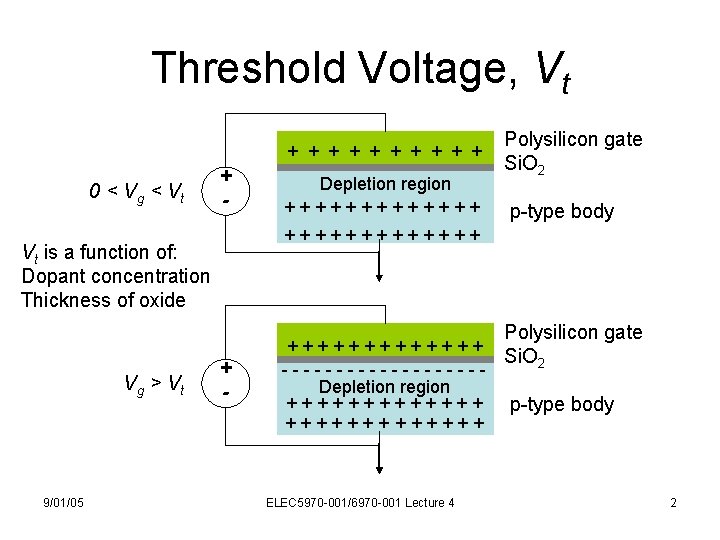
Threshold Voltage, Vt + + + + + 0 < V g < Vt + - 9/01/05 p-type body +++++++ Vt is a function of: Dopant concentration Thickness of oxide Vg > Vt Depletion region +++++++ Polysilicon gate Si. O 2 + - +++++++ ---------Depletion region +++++++ ELEC 5970 -001/6970 -001 Lecture 4 Polysilicon gate Si. O 2 p-type body 2

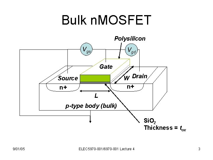
Bulk n. MOSFET Polysilicon Vgs Vgd Gate W Drain n+ Source n+ L p-type body (bulk) Si. O 2 Thickness = tox 9/01/05 ELEC 5970 -001/6970 -001 Lecture 4 3

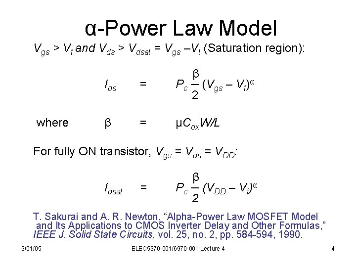
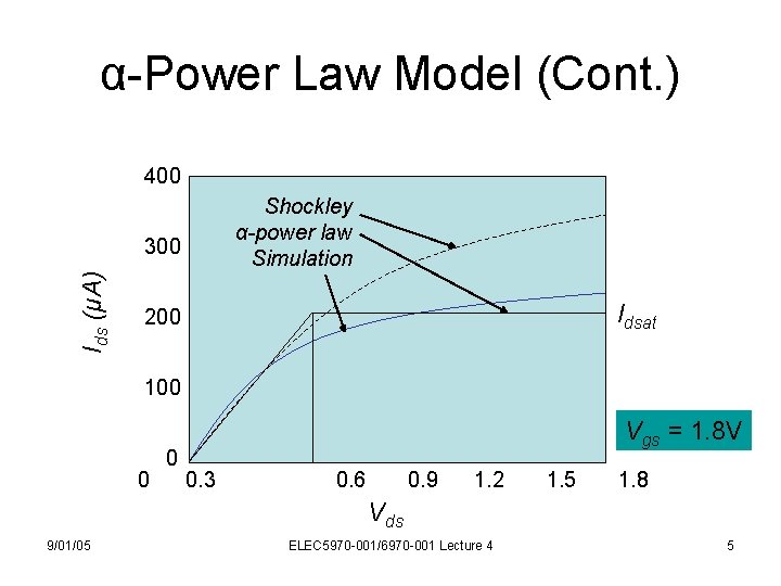
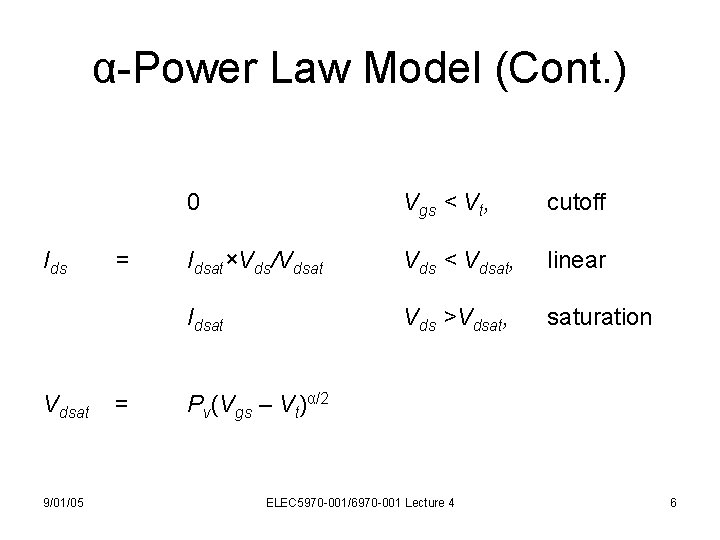
α-Power Law Model Vgs > Vt and Vds > Vdsat = Vgs –Vt (Saturation region): where Ids = β Pc ─ (Vgs – Vt)α 2 β = μCox. W/L For fully ON transistor, Vgs = Vds = VDD: Idsat = β Pc ─ (VDD – Vt)α 2 T. Sakurai and A. R. Newton, “Alpha-Power Law MOSFET Model and Its Applications to CMOS Inverter Delay and Other Formulas, ” IEEE J. Solid State Circuits, vol. 25, no. 2, pp. 584 -594, 1990. 9/01/05 ELEC 5970 -001/6970 -001 Lecture 4 4

α-Power Law Model (Cont. ) 400 Shockley α-power law Simulation Ids (μA) 300 Idsat 200 100 0 0 Vgs = 1. 8 V 0. 3 0. 6 0. 9 1. 2 1. 5 1. 8 Vds 9/01/05 ELEC 5970 -001/6970 -001 Lecture 4 5

α-Power Law Model (Cont. ) Ids Vdsat 9/01/05 = = 0 Vgs < Vt, cutoff Idsat×Vds/Vdsat Vds < Vdsat, linear Idsat Vds >Vdsat, saturation Pv(Vgs – Vt)α/2 ELEC 5970 -001/6970 -001 Lecture 4 6

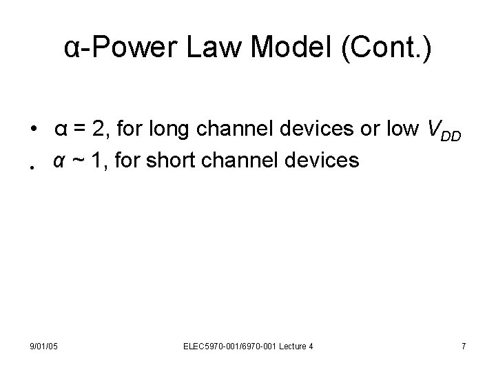
α-Power Law Model (Cont. ) • α = 2, for long channel devices or low VDD • α ~ 1, for short channel devices 9/01/05 ELEC 5970 -001/6970 -001 Lecture 4 7

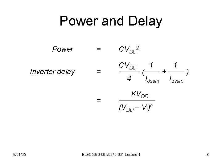
Power and Delay Power Inverter delay 9/01/05 = CVDD 2 = CVDD 1 1 ──── (─── + ─── ) 4 Idsatn Idsatp = KVDD ─────── (VDD – Vt)α ELEC 5970 -001/6970 -001 Lecture 4 8

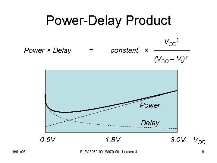
Power-Delay Product Power × Delay = VDD 3 constant × ─────── (VDD – Vt)α Power Delay 0. 6 V 9/01/05 1. 8 V ELEC 5970 -001/6970 -001 Lecture 4 3. 0 V VDD 9

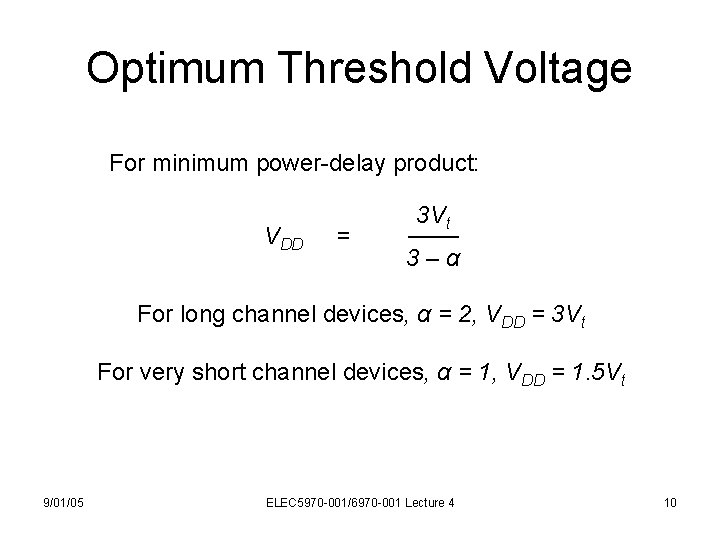
Optimum Threshold Voltage For minimum power-delay product: VDD = 3 Vt ─── 3–α For long channel devices, α = 2, VDD = 3 Vt For very short channel devices, α = 1, VDD = 1. 5 Vt 9/01/05 ELEC 5970 -001/6970 -001 Lecture 4 10

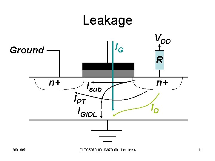
Leakage IG Ground R n+ Isub IPT IGIDL 9/01/05 VDD ELEC 5970 -001/6970 -001 Lecture 4 n+ ID 11

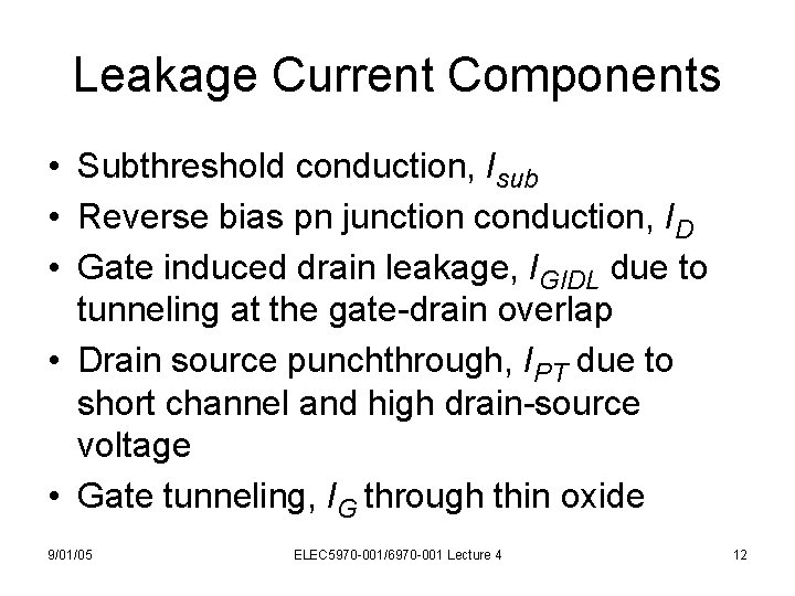
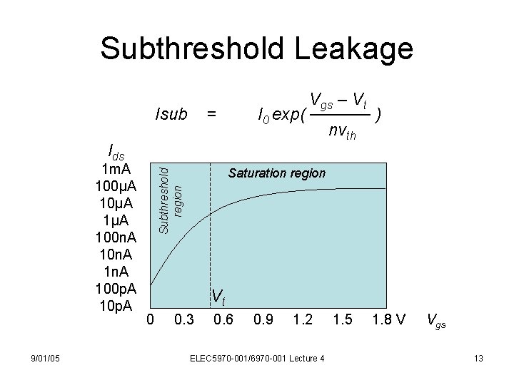
Leakage Current Components • Subthreshold conduction, Isub • Reverse bias pn junction conduction, ID • Gate induced drain leakage, IGIDL due to tunneling at the gate-drain overlap • Drain source punchthrough, IPT due to short channel and high drain-source voltage • Gate tunneling, IG through thin oxide 9/01/05 ELEC 5970 -001/6970 -001 Lecture 4 12

Subthreshold Leakage Isub Vgs – Vt I 0 exp( ───── ) nvth = Ids 9/01/05 Saturation region Subthreshold region 1 m. A 100μA 1μA 100 n. A 1 n. A 100 p. A 10 p. A Vt 0 0. 3 0. 6 0. 9 1. 2 ELEC 5970 -001/6970 -001 Lecture 4 1. 5 1. 8 V Vgs 13

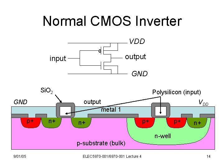
Normal CMOS Inverter VDD o input output GND Si. O 2 output metal 1 GND p+ Polysilicon (input) n+ n+ VDD p+ p+ n+ n-well p-substrate (bulk) 9/01/05 ELEC 5970 -001/6970 -001 Lecture 4 14

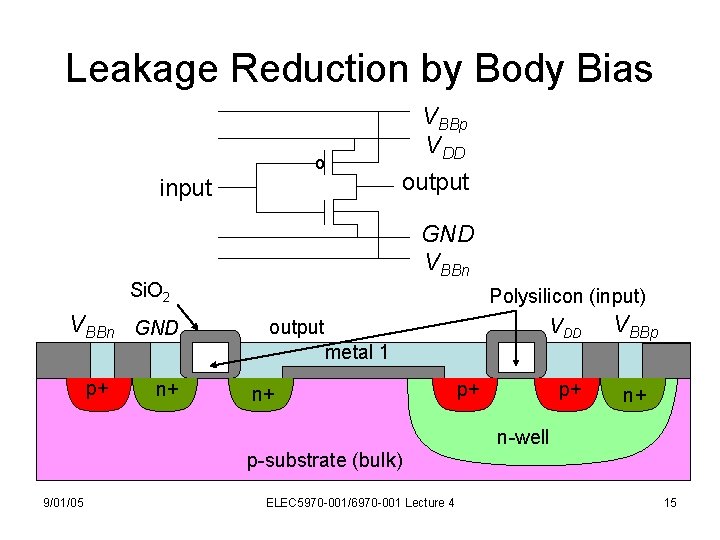
Leakage Reduction by Body Bias o input VBBp VDD output GND VBBn Si. O 2 VBBn GND p+ n+ Polysilicon (input) output metal 1 n+ VDD VBBp p+ n+ p+ n-well p-substrate (bulk) 9/01/05 ELEC 5970 -001/6970 -001 Lecture 4 15

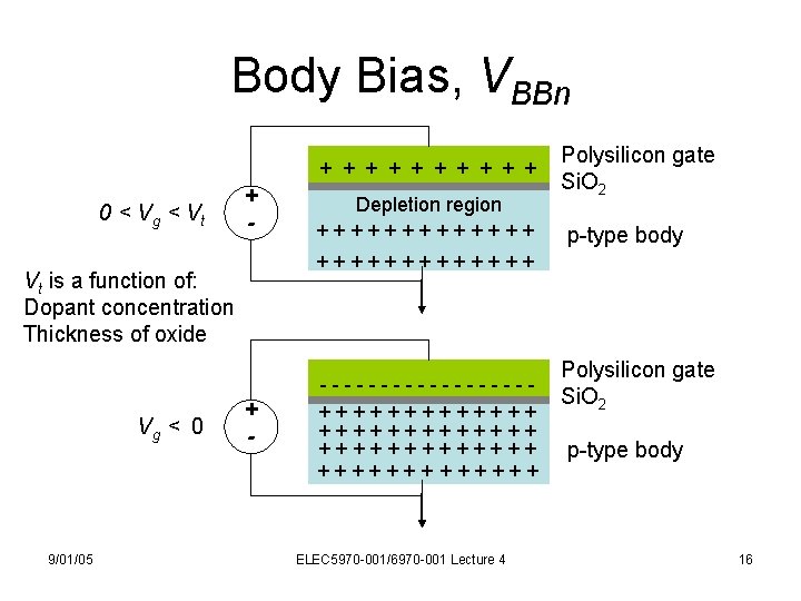
Body Bias, VBBn + + + + + 0 < V g < Vt + - 9/01/05 p-type body +++++++ Vt is a function of: Dopant concentration Thickness of oxide Vg < 0 Depletion region +++++++ Polysilicon gate Si. O 2 + - ---------+++++++++++++ ++++++ ELEC 5970 -001/6970 -001 Lecture 4 Polysilicon gate Si. O 2 p-type body 16

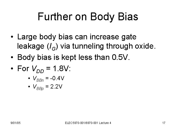
Further on Body Bias • Large body bias can increase gate leakage (IG) via tunneling through oxide. • Body bias is kept less than 0. 5 V. • For VDD = 1. 8 V: • VBBn = -0. 4 V • VBBp = 2. 2 V 9/01/05 ELEC 5970 -001/6970 -001 Lecture 4 17

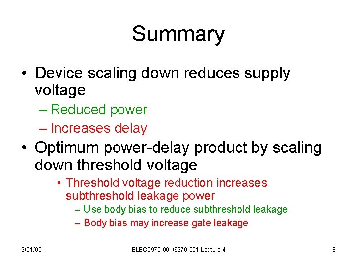
Summary • Device scaling down reduces supply voltage – Reduced power – Increases delay • Optimum power-delay product by scaling down threshold voltage • Threshold voltage reduction increases subthreshold leakage power – Use body bias to reduce subthreshold leakage – Body bias may increase gate leakage 9/01/05 ELEC 5970 -001/6970 -001 Lecture 4 18