ECE 551 Digital System Design Synthesis Lecture Set
- Slides: 67

ECE 551: Digital System Design & Synthesis Lecture Set 10 10. 1: Functional & Timing Verification (Separate File) 10. 2: Faults & Testing 10. 2 Appendix: PODEM Example Slides adapted from ECE 553 Slides by Prof. Kewal Saluja 04/23/2003 1

ECE 551 - Digital System Design & Synthesis Lecture 10. 2 – Faults and Testing Overview Introduction q Fault Models q Test Pattern Generation q Design for Testability (DFT) – Serial Scan q Built-In Self-Test (BIST) q Boundary Scan (JTAG/IEEE 1149. 1) q Quiescent Drain Current (IDDQ) Testing q 04/23/2003 2

Introduction The manufacturing process for ICs is so complex that only a portion of all chips produced are good – the percentage of such good chips is referred to as the yield q In order to avoid shipping defective products, manufacturing test at the die and packaged chip level is required. q Complex chips => complex tests q q The objective: summary the elements of contemporary IC test 04/23/2003 3

Overview Introduction q Fault Models q Test Pattern Generation q Design for Testability (DFT) – Serial Scan q Built-In Self-Test (BIST) q Boundary Scan (JTAG/IEEE 1149. 1) q Quiescent Drain Current (IDDQ) Testing q 04/23/2003 4

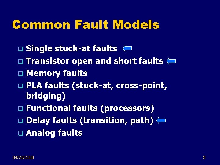
Common Fault Models Single stuck-at faults q Transistor open and short faults q Memory faults q PLA faults (stuck-at, cross-point, bridging) q Functional faults (processors) q Delay faults (transition, path) q Analog faults q 04/23/2003 5

Stuck-at Faults • Single stuck-at fault model • What does it achieve in practice? • Fault equivalence • Checkpoint faults 04/23/2003 6

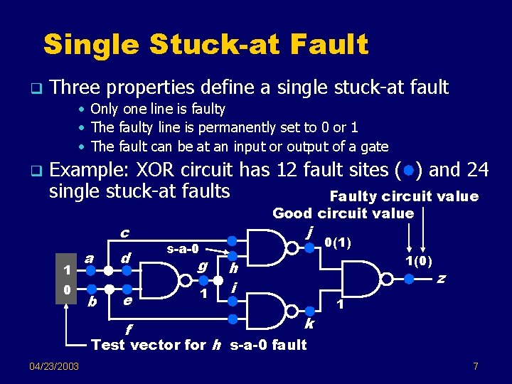
Single Stuck-at Fault q Three properties define a single stuck-at fault • Only one line is faulty • The faulty line is permanently set to 0 or 1 • The fault can be at an input or output of a gate q Example: XOR circuit has 12 fault sites ( ) and 24 single stuck-at faults Faulty circuit value c 1 0 a d b e f Good circuit value j s-a-0 g 1 0(1) 1(0) h i k z 1 Test vector for h s-a-0 fault 04/23/2003 7

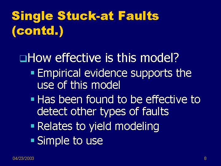
Single Stuck-at Faults (contd. ) q. How effective is this model? § Empirical evidence supports the use of this model § Has been found to be effective to detect other types of faults § Relates to yield modeling § Simple to use 04/23/2003 8

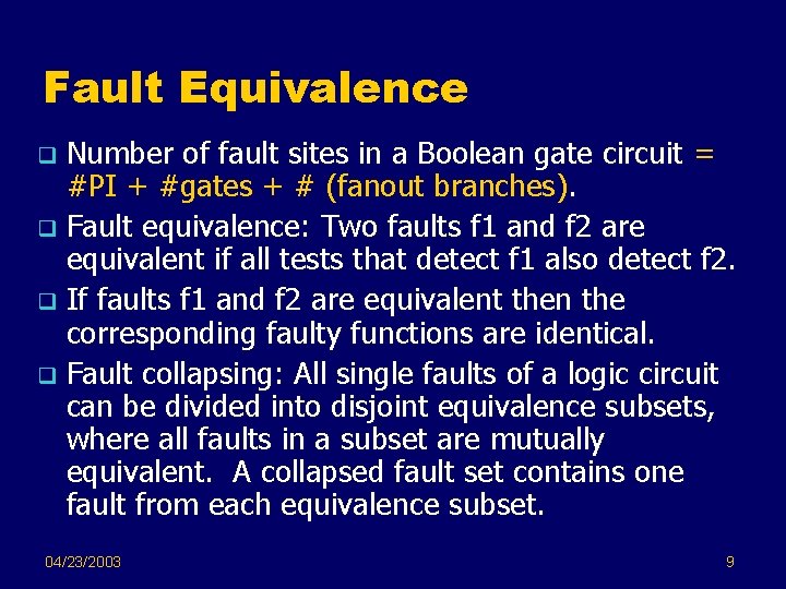
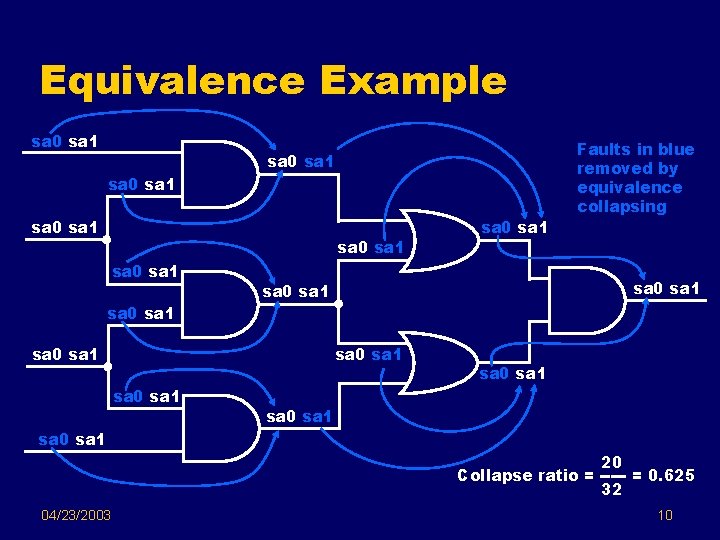
Fault Equivalence Number of fault sites in a Boolean gate circuit = #PI + #gates + # (fanout branches). q Fault equivalence: Two faults f 1 and f 2 are equivalent if all tests that detect f 1 also detect f 2. q If faults f 1 and f 2 are equivalent then the corresponding faulty functions are identical. q Fault collapsing: All single faults of a logic circuit can be divided into disjoint equivalence subsets, where all faults in a subset are mutually equivalent. A collapsed fault set contains one fault from each equivalence subset. q 04/23/2003 9

Equivalence Example sa 0 sa 1 sa 0 sa 1 04/23/2003 sa 0 sa 1 sa 0 sa 1 Faults in blue removed by equivalence collapsing sa 0 sa 1 20 Collapse ratio = ----- = 0. 625 32 10

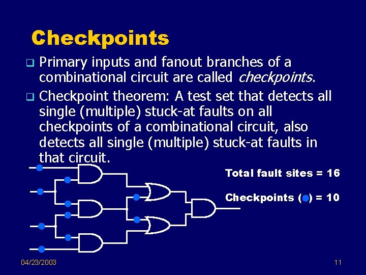
Checkpoints Primary inputs and fanout branches of a combinational circuit are called checkpoints. q Checkpoint theorem: A test set that detects all single (multiple) stuck-at faults on all checkpoints of a combinational circuit, also detects all single (multiple) stuck-at faults in that circuit. q Total fault sites = 16 Checkpoints ( ) = 10 04/23/2003 11

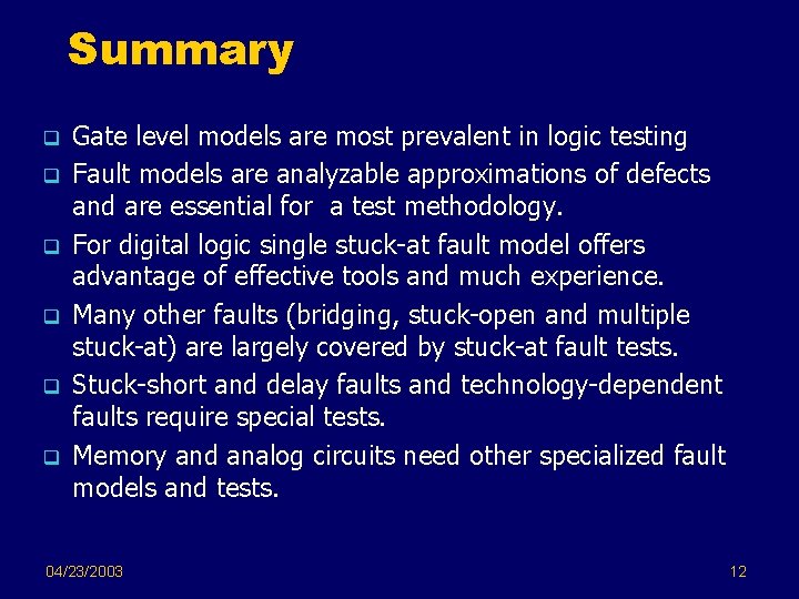
Summary q q q Gate level models are most prevalent in logic testing Fault models are analyzable approximations of defects and are essential for a test methodology. For digital logic single stuck-at fault model offers advantage of effective tools and much experience. Many other faults (bridging, stuck-open and multiple stuck-at) are largely covered by stuck-at fault tests. Stuck-short and delay faults and technology-dependent faults require special tests. Memory and analog circuits need other specialized fault models and tests. 04/23/2003 12

Overview Introduction q Fault Models q Test Pattern Generation q Design for Testability (DFT) – Serial Scan q Built-In Self-Test (BIST) q Boundary Scan (JTAG/IEEE 1149. 1) q Quiescent Drain Current (IDDQ) Testing q 04/23/2003 13

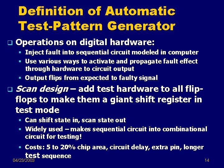
Definition of Automatic Test-Pattern Generator q Operations on digital hardware: § Inject fault into sequential circuit modeled in computer § Use various ways to activate and propagate fault effect through hardware to circuit output § Output flips from expected to faulty signal q Scan design – add test hardware to all flipflops to make them a giant shift register in test mode § Can shift state in, scan state out § Widely used – makes sequential circuit into combinational circuit for testing! § Costs: 5 to 20% chip area, circuit delay, extra pin, longer test sequence 04/23/2003 14

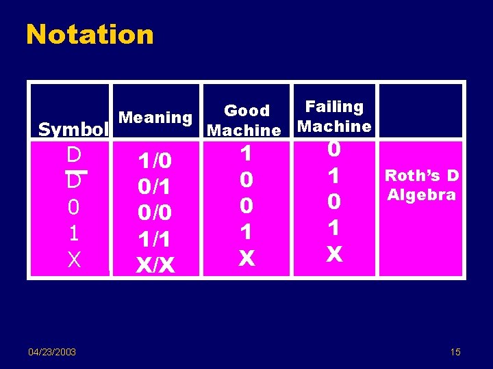
Notation Failing Good Meaning Machine Symbol D D 0 1 X 04/23/2003 1/0 0/1 0/0 1/1 X/X 1 0 0 1 X Roth’s D Algebra 15

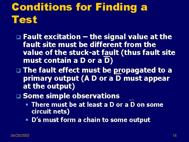
Conditions for Finding a Test Fault excitation – the signal value at the fault site must be different from the value of the stuck-at fault (thus fault site must contain a D or a D) q The fault effect must be propagated to a primary output (A D or a D must appear at the output) q Some simple observations q § There must be at least a D or a D on some circuit nets) § D’s must form a chain to some output 04/23/2003 16

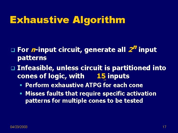
Exhaustive Algorithm For n-input circuit, generate all 2 n input patterns q Infeasible, unless circuit is partitioned into cones of logic, with 15 inputs q § Perform exhaustive ATPG for each cone § Misses faults that require specific activation patterns for multiple cones to be tested 04/23/2003 17

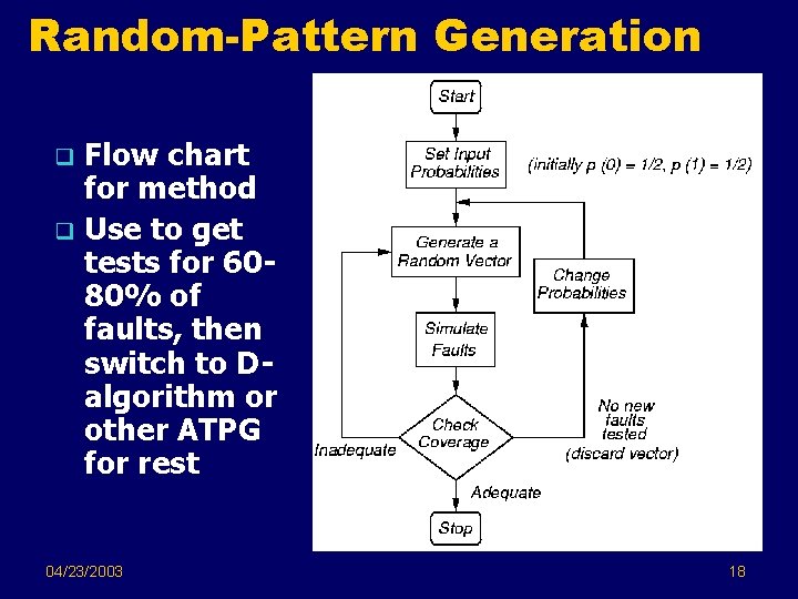
Random-Pattern Generation Flow chart for method q Use to get tests for 6080% of faults, then switch to Dalgorithm or other ATPG for rest q 04/23/2003 18

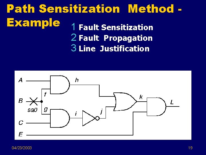
Path Sensitization Method Example 1 Fault Sensitization 2 Fault Propagation 3 Line Justification 04/23/2003 19

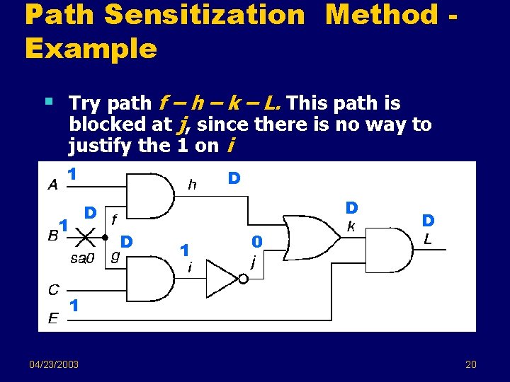
Path Sensitization Method Example § Try path f – h – k – L. This path is blocked at j, since there is no way to justify the 1 on i 1 1 D D 1 04/23/2003 20

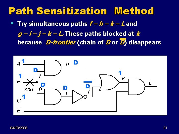
Path Sensitization Method § Try simultaneous paths f – h – k – L and g – i – j – k – L. These paths blocked at k because D-frontier (chain of D or D) disappears 1 1 D D D 1 04/23/2003 21

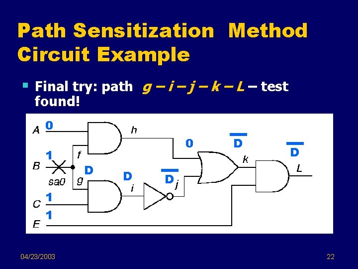
Path Sensitization Method Circuit Example § Final try: path g – i – j – k – L – test found! 0 1 0 D D D 1 1 04/23/2003 22

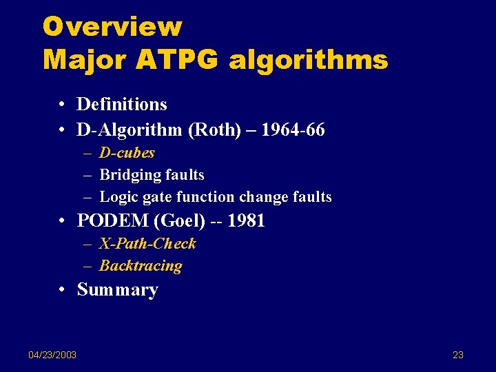
Overview Major ATPG algorithms • Definitions • D-Algorithm (Roth) – 1964 -66 – D-cubes – Bridging faults – Logic gate function change faults • PODEM (Goel) -- 1981 – X-Path-Check – Backtracing • Summary 04/23/2003 23

Overview Introduction q Fault Models q Test Pattern Generation q Design for Testability (DFT) – Serial Scan q Built-In Self-Test (BIST) q Boundary Scan (JTAG/IEEE 1149. 1) q Quiescent Drain Current (IDDQ) Testing q 04/23/2003 24

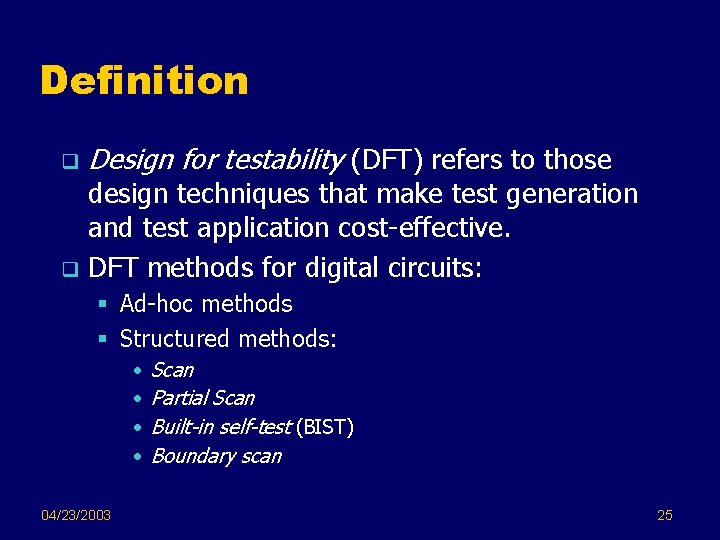
Definition q Design for testability (DFT) refers to those design techniques that make test generation and test application cost-effective. q DFT methods for digital circuits: § Ad-hoc methods § Structured methods: • • 04/23/2003 Scan Partial Scan Built-in self-test (BIST) Boundary scan 25

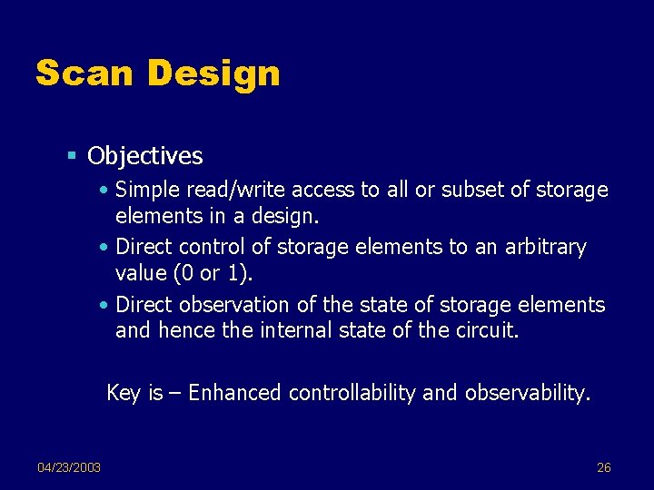
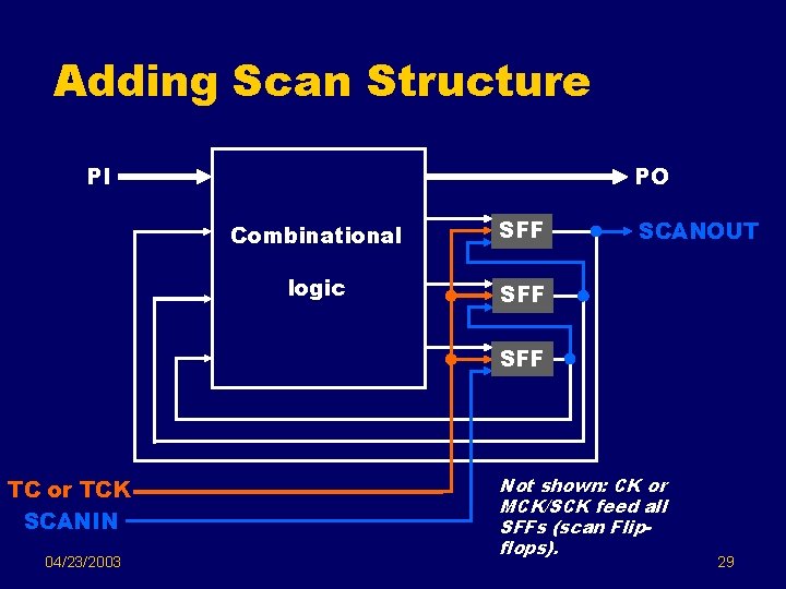
Scan Design § Objectives • Simple read/write access to all or subset of storage elements in a design. • Direct control of storage elements to an arbitrary value (0 or 1). • Direct observation of the state of storage elements and hence the internal state of the circuit. Key is – Enhanced controllability and observability. 04/23/2003 26

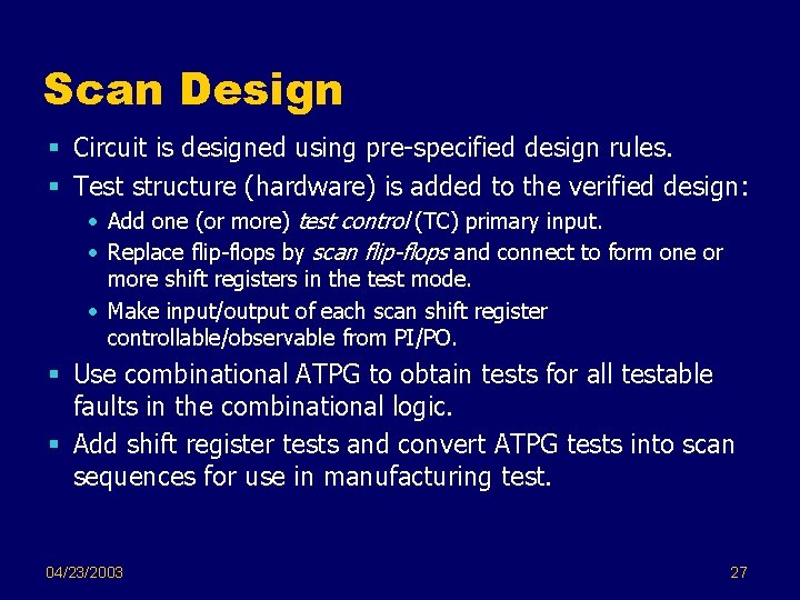
Scan Design § Circuit is designed using pre-specified design rules. § Test structure (hardware) is added to the verified design: • Add one (or more) test control (TC) primary input. • Replace flip-flops by scan flip-flops and connect to form one or more shift registers in the test mode. • Make input/output of each scan shift register controllable/observable from PI/PO. § Use combinational ATPG to obtain tests for all testable faults in the combinational logic. § Add shift register tests and convert ATPG tests into scan sequences for use in manufacturing test. 04/23/2003 27

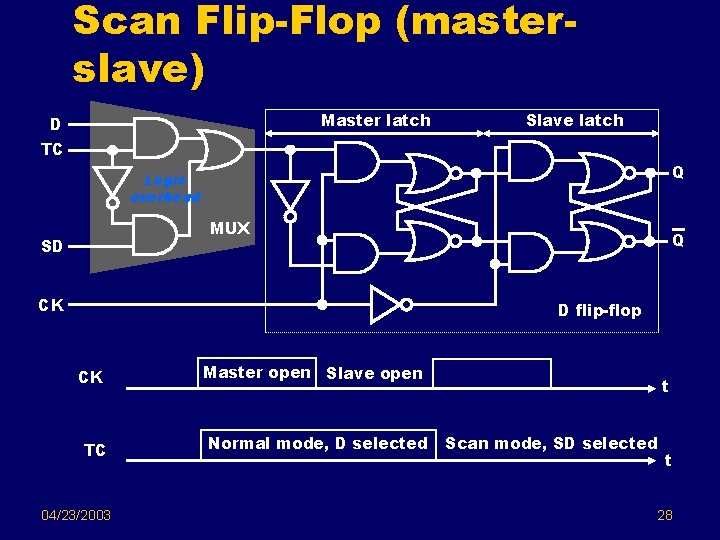
Scan Flip-Flop (masterslave) Master latch D Slave latch TC Q Logic overhead MUX SD CK Q D flip-flop CK TC 04/23/2003 Master open Slave open Normal mode, D selected t Scan mode, SD selected t 28

Adding Scan Structure PI PO Combinational SFF logic SFF SCANOUT SFF TC or TCK SCANIN 04/23/2003 Not shown: CK or MCK/SCK feed all SFFs (scan Flipflops). 29

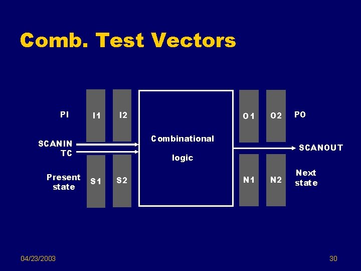
Comb. Test Vectors PI I 1 I 2 04/23/2003 O 2 Combinational SCANIN TC Present state O 1 SCANOUT logic S 1 S 2 PO N 1 N 2 Next state 30

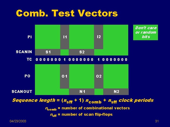
Comb. Test Vectors SCANIN I 2 I 1 PI S 1 Don’t care or random bits S 2 TC 0 0 0 0 1 0 0 0 0 PO SCANOUT O 2 O 1 N 2 Sequence length = (nsff + 1) ncomb + nsff clock periods ncomb = number of combinational vectors nsff = number of scan flip-flops 04/23/2003 31

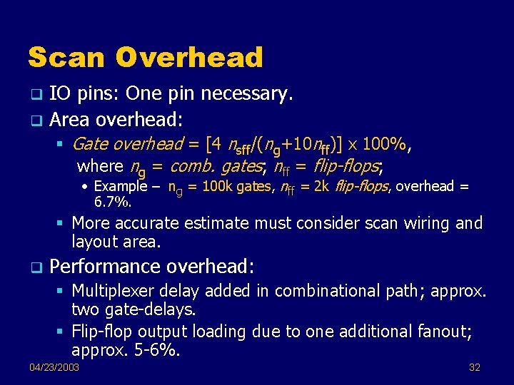
Scan Overhead IO pins: One pin necessary. q Area overhead: q § Gate overhead = [4 nsff/(ng+10 nff)] x 100%, where ng = comb. gates; nff = flip-flops; • Example – ng = 100 k gates, nff = 2 k flip-flops, overhead = 6. 7%. § More accurate estimate must consider scan wiring and layout area. q Performance overhead: § Multiplexer delay added in combinational path; approx. two gate-delays. § Flip-flop output loading due to one additional fanout; approx. 5 -6%. 04/23/2003 32

Overview Introduction q Fault Models q Test Pattern Generation q Design for Testability (DFT) – Serial Scan q Built-In Self-Test (BIST) q Boundary Scan (JTAG/IEEE 1149. 1) q Quiescent Drain Current (IDDQ) Testing q 04/23/2003 33

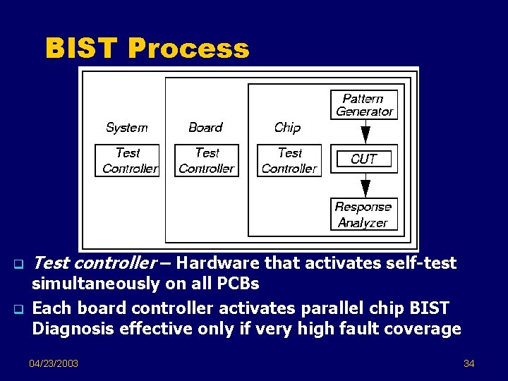
BIST Process q q Test controller – Hardware that activates self-test simultaneously on all PCBs Each board controller activates parallel chip BIST Diagnosis effective only if very high fault coverage 04/23/2003 34

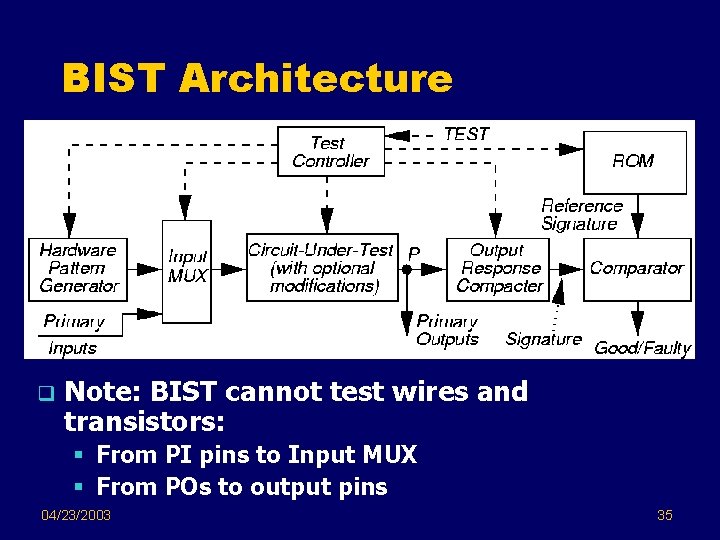
BIST Architecture q Note: BIST cannot test wires and transistors: § From PI pins to Input MUX § From POs to output pins 04/23/2003 35

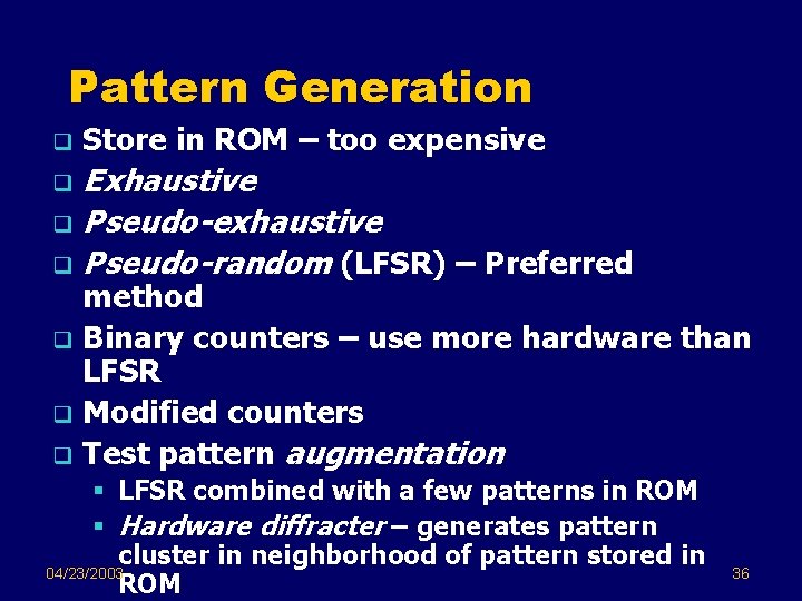
Pattern Generation q Store in ROM – too expensive Exhaustive q Pseudo-exhaustive q Pseudo-random (LFSR) – Preferred q method q Binary counters – use more hardware than LFSR q Modified counters q Test pattern augmentation § LFSR combined with a few patterns in ROM § Hardware diffracter – generates pattern cluster in neighborhood of pattern stored in 04/23/2003 ROM 36

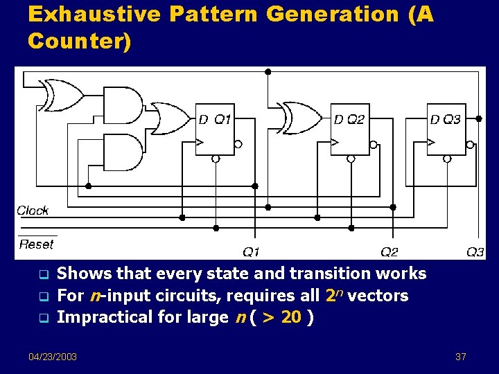
Exhaustive Pattern Generation (A Counter) q q q Shows that every state and transition works For n-input circuits, requires all 2 n vectors Impractical for large n ( > 20 ) 04/23/2003 37

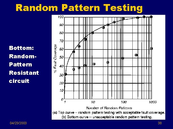
Random Pattern Testing Bottom: Random. Pattern Resistant circuit 04/23/2003 38

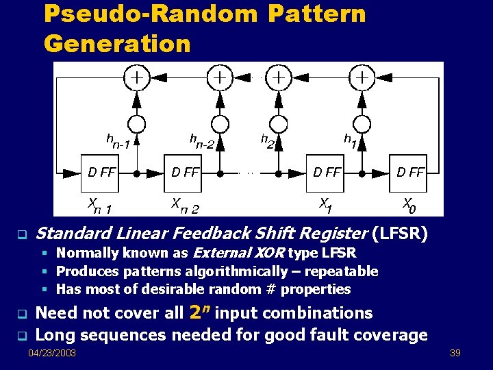
Pseudo-Random Pattern Generation q Standard Linear Feedback Shift Register (LFSR) § Normally known as External XOR type LFSR § Produces patterns algorithmically – repeatable § Has most of desirable random # properties q Need not cover all 2 n input combinations q Long sequences needed for good fault coverage 04/23/2003 39

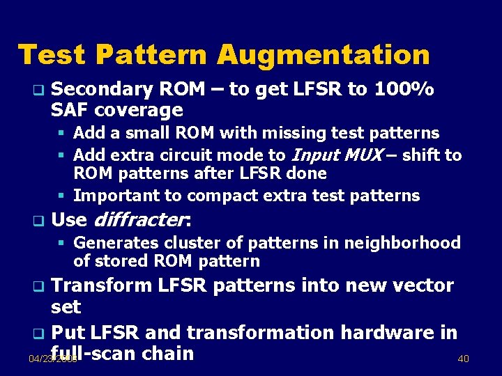
Test Pattern Augmentation q Secondary ROM – to get LFSR to 100% SAF coverage § Add a small ROM with missing test patterns § Add extra circuit mode to Input MUX – shift to ROM patterns after LFSR done § Important to compact extra test patterns q Use diffracter: § Generates cluster of patterns in neighborhood of stored ROM pattern Transform LFSR patterns into new vector set q Put LFSR and transformation hardware in full-scan chain 04/23/2003 40 q

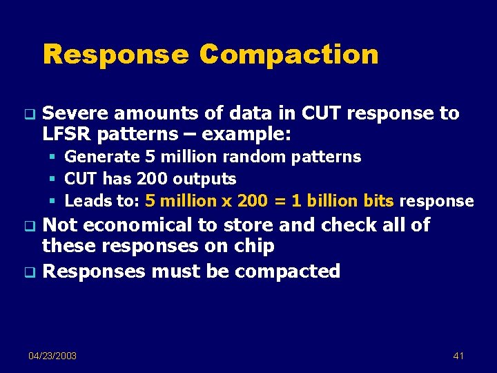
Response Compaction q Severe amounts of data in CUT response to LFSR patterns – example: § Generate 5 million random patterns § CUT has 200 outputs § Leads to: 5 million x 200 = 1 billion bits response Not economical to store and check all of these responses on chip q Responses must be compacted q 04/23/2003 41

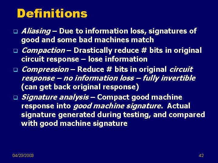
Definitions q q Aliasing – Due to information loss, signatures of good and some bad machines match Compaction – Drastically reduce # bits in original circuit response – lose information Compression – Reduce # bits in original circuit response – no information loss – fully invertible (can get back original response) Signature analysis – Compact good machine response into good machine signature. Actual signature generated during testing, and compared with good machine signature 04/23/2003 42

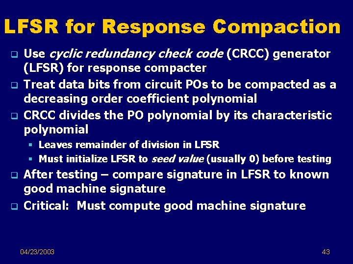
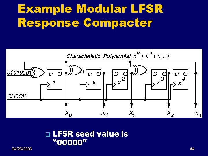
LFSR for Response Compaction q q q Use cyclic redundancy check code (CRCC) generator (LFSR) for response compacter Treat data bits from circuit POs to be compacted as a decreasing order coefficient polynomial CRCC divides the PO polynomial by its characteristic polynomial § Leaves remainder of division in LFSR § Must initialize LFSR to seed value (usually 0) before testing q q After testing – compare signature in LFSR to known good machine signature Critical: Must compute good machine signature 04/23/2003 43

Example Modular LFSR Response Compacter q 04/23/2003 LFSR seed value is “ 00000” 44

Summary LFSR pattern generator and MISR response compacter – preferred BIST methods q BIST has overheads: test controller, extra circuit delay, Input MUX, pattern generator, response compacter, DFT to initialize circuit & test the test hardware q BIST benefits: q § § § At-speed testing for delay & stuck-at faults Drastic ATE cost reduction Field test capability Faster diagnosis during system test Less effort to design testing process Shorter test application times 04/23/2003 45

Overview Introduction q Fault Models q Test Pattern Generation q Design for Testability (DFT) – Serial Scan q Built-In Self-Test (BIST) q Boundary Scan (JTAG/IEEE 1149. 1) q Quiescent Drain Current (IDDQ) Testing q 04/23/2003 46

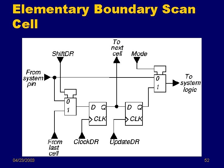
Overview: Boundary Scan Motivation q System view of boundary scan hardware q Elementary scan cell q Test Access Port (TAP) controller q Boundary scan instructions q Summary q 04/23/2003 47

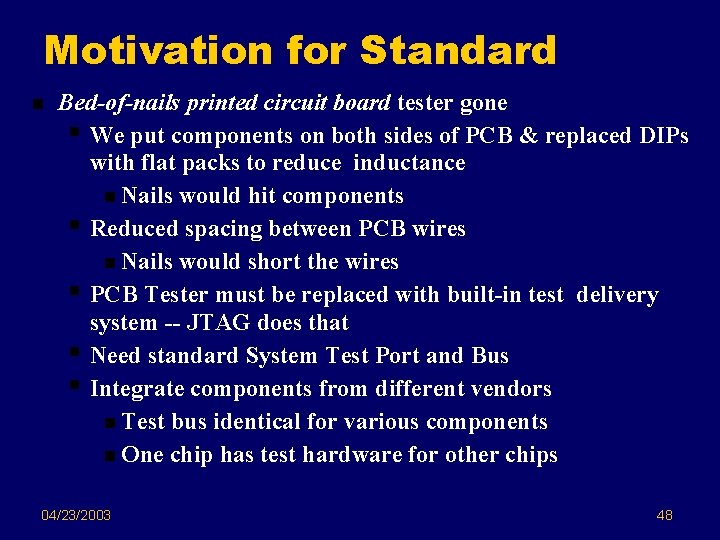
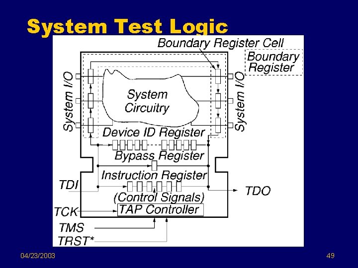
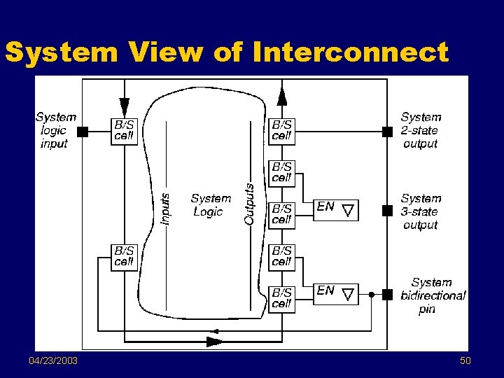
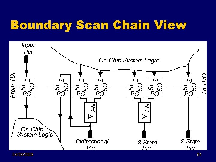
Motivation for Standard n Bed-of-nails printed circuit board tester gone § We put components on both sides of PCB & replaced DIPs with flat packs to reduce inductance n Nails would hit components § Reduced spacing between PCB wires n Nails would short the wires § PCB Tester must be replaced with built-in test delivery system -- JTAG does that § Need standard System Test Port and Bus § Integrate components from different vendors n Test bus identical for various components n One chip has test hardware for other chips 04/23/2003 48

System Test Logic 04/23/2003 49

System View of Interconnect 04/23/2003 50

Boundary Scan Chain View 04/23/2003 51

Elementary Boundary Scan Cell 04/23/2003 52

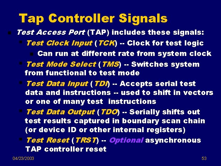
Tap Controller Signals n Test Access Port (TAP) includes these signals: § Test Clock Input (TCK) -- Clock for test logic Can run at different rate from system clock Test Mode Select (TMS) -- Switches system from functional to test mode Test Data Input (TDI) -- Accepts serial test data and instructions -- used to shift in vectors or one of many test instructions Test Data Output (TDO) -- Serially shifts out test results captured in boundary scan chain (or device ID or other internal registers) Test Reset (TRST) -- Optional asynchronous TAP controller reset n § § 04/23/2003 53

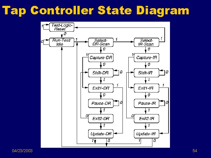
Tap Controller State Diagram 04/23/2003 54

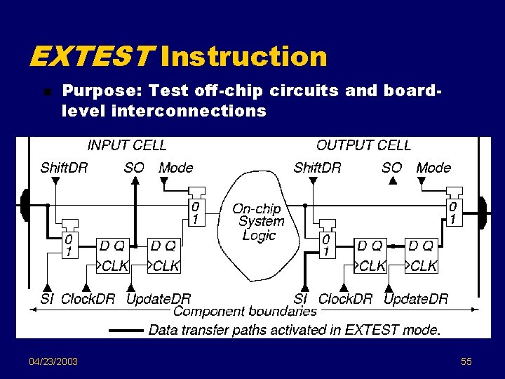
EXTEST Instruction n Purpose: Test off-chip circuits and boardlevel interconnections 04/23/2003 55

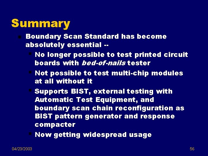
Summary n Boundary Scan Standard has become absolutely essential -§ No longer possible to test printed circuit boards with bed-of-nails tester § Not possible to test multi-chip modules at all without it § Supports BIST, external testing with Automatic Test Equipment, and boundary scan chain reconfiguration as BIST pattern generator and response compacter § Now getting widespread usage 04/23/2003 56

Overview Introduction q Fault Models q Test Pattern Generation q Design for Testability (DFT) – Serial Scan q Built-In Self-Test (BIST) q Boundary Scan (JTAG/IEEE 1149. 1) q Quiescent Drain Current (IDDQ) Testing q 04/23/2003 57

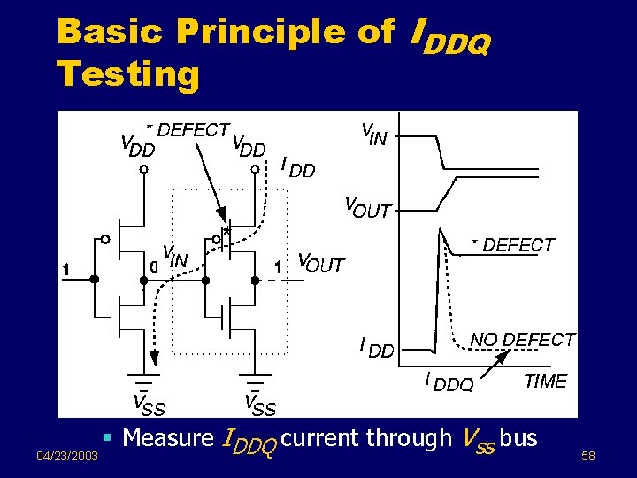
Basic Principle of IDDQ Testing 04/23/2003 § Measure IDDQ current through Vss bus 58

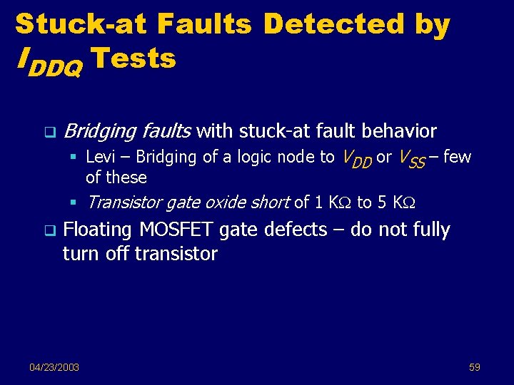
Stuck-at Faults Detected by IDDQ Tests q Bridging faults with stuck-at fault behavior § Levi – Bridging of a logic node to VDD or VSS – few of these § Transistor gate oxide short of 1 KW to 5 KW q Floating MOSFET gate defects – do not fully turn off transistor 04/23/2003 59

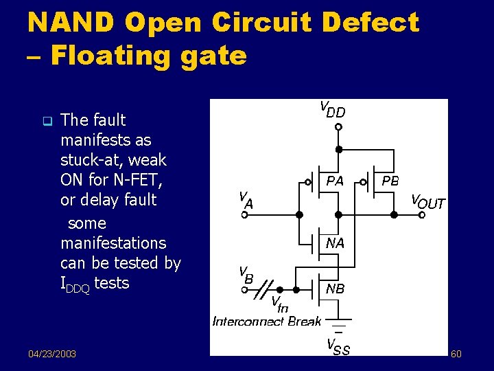
NAND Open Circuit Defect – Floating gate q The fault manifests as stuck-at, weak ON for N-FET, or delay fault some manifestations can be tested by IDDQ tests 04/23/2003 60

Floating Gate Defects q Small break in logic gate inputs (100 – 200 Angstroms) lets wires couple by electron tunneling § Delay fault and IDDQ fault q Large open results in stuck-at fault – not detectable by IDDQ test 04/23/2003 61

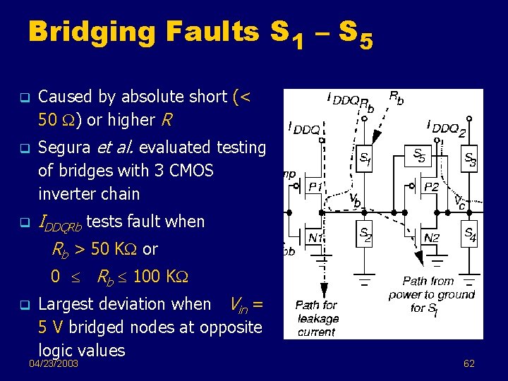
Bridging Faults S 1 – S 5 q Caused by absolute short (< 50 W) or higher R q Segura et al. evaluated testing of bridges with 3 CMOS inverter chain q IDDQRb tests fault when Rb > 50 KW or 0 Rb 100 KW q Largest deviation when Vin = 5 V bridged nodes at opposite logic values 04/23/2003 62

Delay Faults Most random CMOS defects cause a timing delay fault, not catastrophic failure q Many delay faults detected by IDDQ test – late switching of logic gates keeps IDDQ elevated q Delay faults not detected by IDDQ test q § Resistive via fault in interconnect § Increased transistor threshold voltage fault 04/23/2003 63

Leakage Faults q Gate oxide shorts cause leaks between gate & source or gate & drain Weak Faults • n. FET passes logic 1 as 5 V – Vtn • p. FET passes logic 0 as 0 V + |Vtp| • Weak fault – one device in C-switch does not turn on § Causes logic value degradation in C-switch 04/23/2003 64

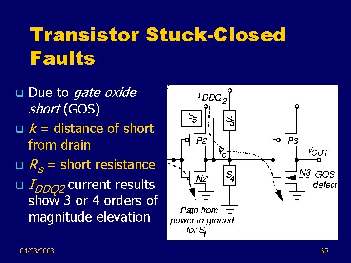
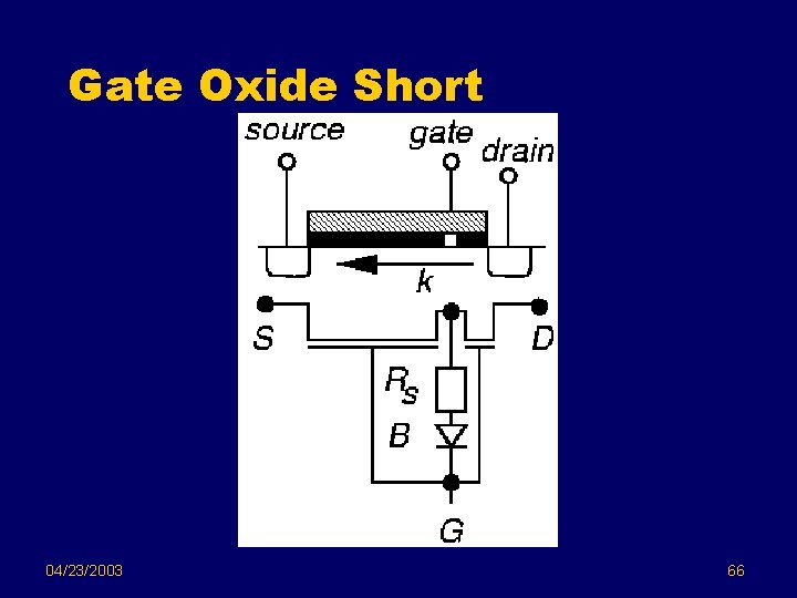
Transistor Stuck-Closed Faults Due to gate oxide short (GOS) q k = distance of short from drain q Rs = short resistance q IDDQ 2 current results show 3 or 4 orders of magnitude elevation q 04/23/2003 65

Gate Oxide Short 04/23/2003 66

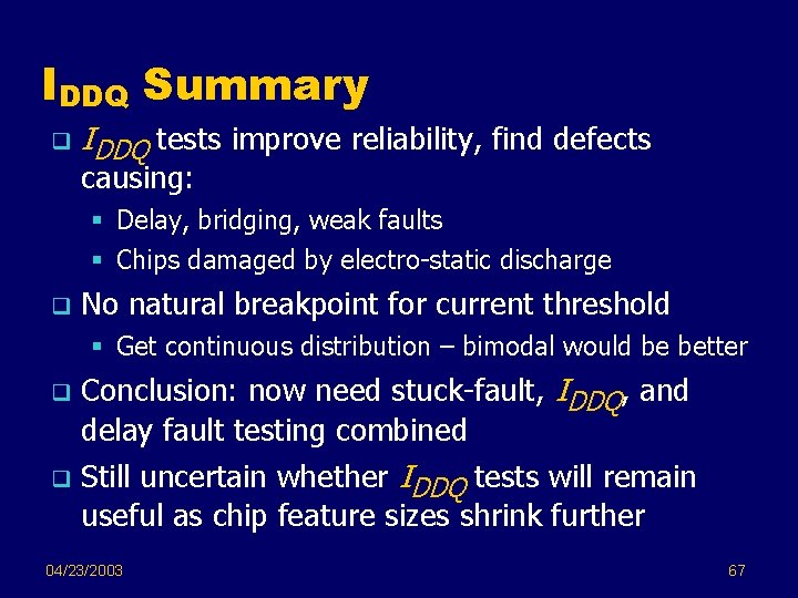
IDDQ Summary q IDDQ tests improve reliability, find defects causing: § Delay, bridging, weak faults § Chips damaged by electro-static discharge q No natural breakpoint for current threshold § Get continuous distribution – bimodal would be better Conclusion: now need stuck-fault, IDDQ, and delay fault testing combined q Still uncertain whether IDDQ tests will remain useful as chip feature sizes shrink further q 04/23/2003 67