ECE 551 Digital System Design Synthesis Spring 2003
![IC Costs - 1 q An example: 10, 000 gate circuit [1] o Fixed IC Costs - 1 q An example: 10, 000 gate circuit [1] o Fixed](https://slidetodoc.com/presentation_image_h/d83ac13b4f1aff800cc9d8e2828d5a85/image-19.jpg)
![References [1] Chris J. Myers, Asynchronous Circuit Design, John Wiley & Sons, Inc. , References [1] Chris J. Myers, Asynchronous Circuit Design, John Wiley & Sons, Inc. ,](https://slidetodoc.com/presentation_image_h/d83ac13b4f1aff800cc9d8e2828d5a85/image-55.jpg)
- Slides: 55

ECE 551: Digital System Design & Synthesis Spring 2003 Lecture Materials Prepared by: Charles Kime, Kewal Saluja and Michael Schulte 1

ECE 551: Digital System Design & Synthesis q. Lecture Set 1: o Introduction o Overview of Contemporary Digital Design o Pragmatics 1 1/16/2003 ECE 551 Spring 2003 2

ECE 551 - Digital System Design & Synthesis Lecture 1. 1 - Introduction q Overview o Course 1/16/2003 Purpose Topics Tools Info ECE 551 Spring 2003 3

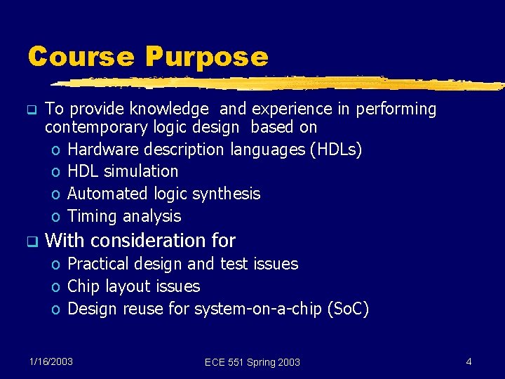
Course Purpose q To provide knowledge and experience in performing contemporary logic design based on o Hardware description languages (HDLs) o HDL simulation o Automated logic synthesis o Timing analysis q With consideration for o Practical design and test issues o Chip layout issues o Design reuse for system-on-a-chip (So. C) 1/16/2003 ECE 551 Spring 2003 4

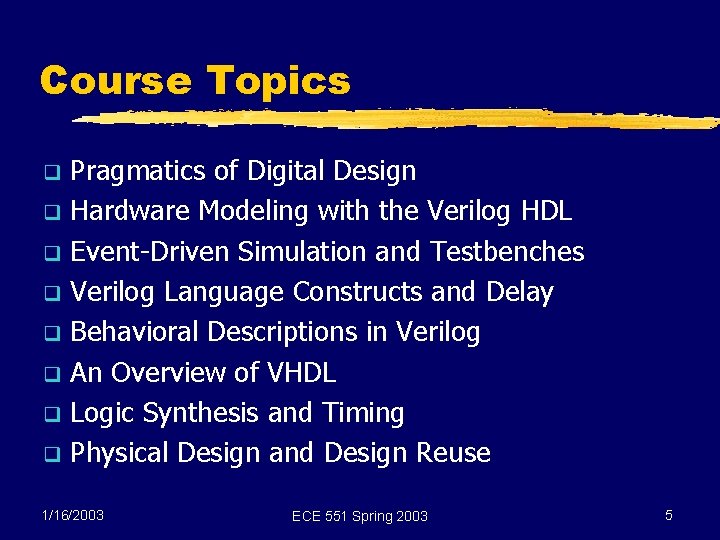
Course Topics Pragmatics of Digital Design q Hardware Modeling with the Verilog HDL q Event-Driven Simulation and Testbenches q Verilog Language Constructs and Delay q Behavioral Descriptions in Verilog q An Overview of VHDL q Logic Synthesis and Timing q Physical Design and Design Reuse q 1/16/2003 ECE 551 Spring 2003 5

Course Tools q Modelsim HDL Simulation Tools (Mentor) q Design Analyzer Synthesis Tools (Synopsys) q G 11 Technology Library (LSI Logic) 1/16/2003 ECE 551 Spring 2003 6

Course Information q Course Conduct q Standard Reference q The above plus all other course material can be found at http: //courses. engr. wisc. edu/ecow/g et/ece/551/kime/ q Be familiar with all! 1/16/2003 ECE 551 Spring 2003 7

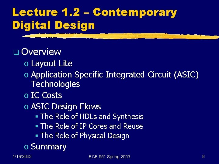
Lecture 1. 2 – Contemporary Digital Design q Overview o Layout Lite o Application Specific Integrated Circuit (ASIC) Technologies o IC Costs o ASIC Design Flows § The Role of HDLs and Synthesis § The Role of IP Cores and Reuse § The Role of Physical Design o Summary 1/16/2003 ECE 551 Spring 2003 8

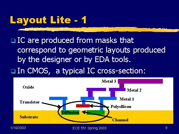
Layout Lite - 1 q IC are produced from masks that correspond to geometric layouts produced by the designer or by EDA tools. q In CMOS, a typical IC cross-section: Metal 3 Oxide Metal 2 Metal 1 Transistor Substrate 1/16/2003 Polysilicon Diffusion Channel ECE 551 Spring 2003 9

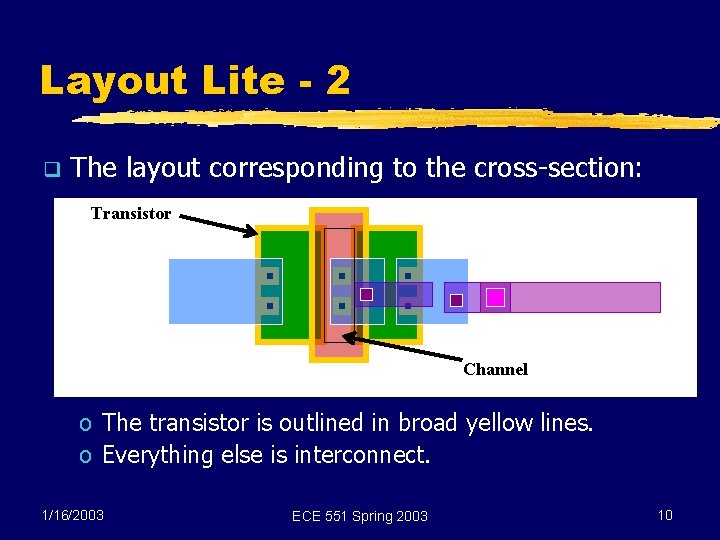
Layout Lite - 2 q The layout corresponding to the cross-section: Transistor Channel o The transistor is outlined in broad yellow lines. o Everything else is interconnect. 1/16/2003 ECE 551 Spring 2003 10

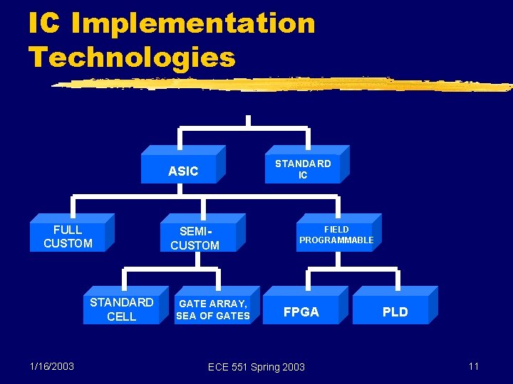
IC Implementation Technologies STANDARD IC ASIC FULL CUSTOM STANDARD CELL 1/16/2003 SEMICUSTOM GATE ARRAY, SEA OF GATES FIELD PROGRAMMABLE FPGA ECE 551 Spring 2003 PLD 11

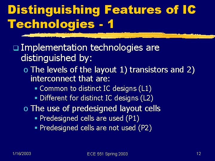
Distinguishing Features of IC Technologies - 1 q Implementation technologies are distinguished by: o The levels of the layout 1) transistors and 2) interconnect that are: § Common to distinct IC designs (L 1) § Different for distinct IC designs (L 2) o The use of predesigned layout cells § Predesigned cells are used (P 1) § Predesigned cells are not used (P 2) 1/16/2003 ECE 551 Spring 2003 12

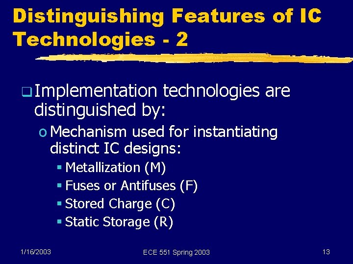
Distinguishing Features of IC Technologies - 2 q Implementation technologies are distinguished by: o Mechanism used for instantiating distinct IC designs: § Metallization (M) § Fuses or Antifuses (F) § Stored Charge (C) § Static Storage (R) 1/16/2003 ECE 551 Spring 2003 13

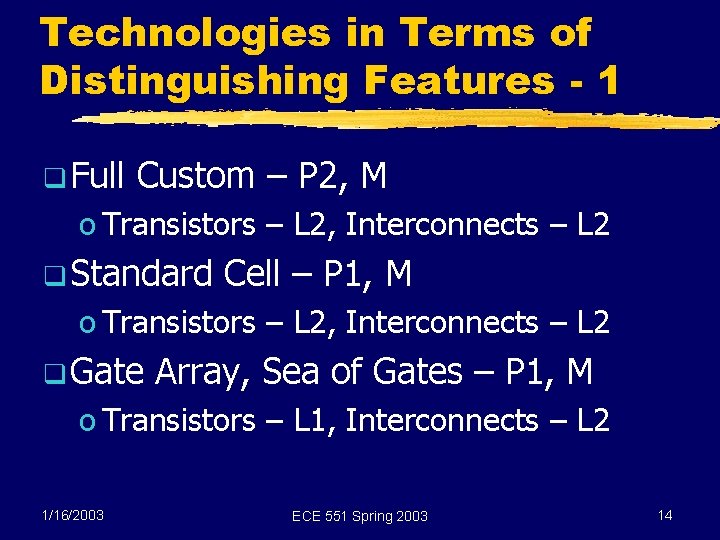
Technologies in Terms of Distinguishing Features - 1 q Full Custom – P 2, M o Transistors – L 2, Interconnects – L 2 q Standard Cell – P 1, M o Transistors – L 2, Interconnects – L 2 q Gate Array, Sea of Gates – P 1, M o Transistors – L 1, Interconnects – L 2 1/16/2003 ECE 551 Spring 2003 14

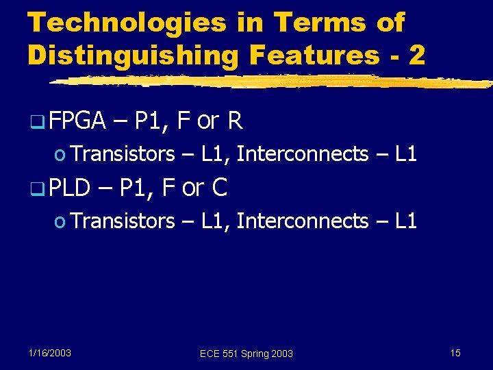
Technologies in Terms of Distinguishing Features - 2 q FPGA – P 1, F or R o Transistors – L 1, Interconnects – L 1 q PLD – P 1, F or C o Transistors – L 1, Interconnects – L 1 1/16/2003 ECE 551 Spring 2003 15

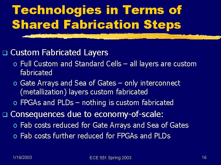
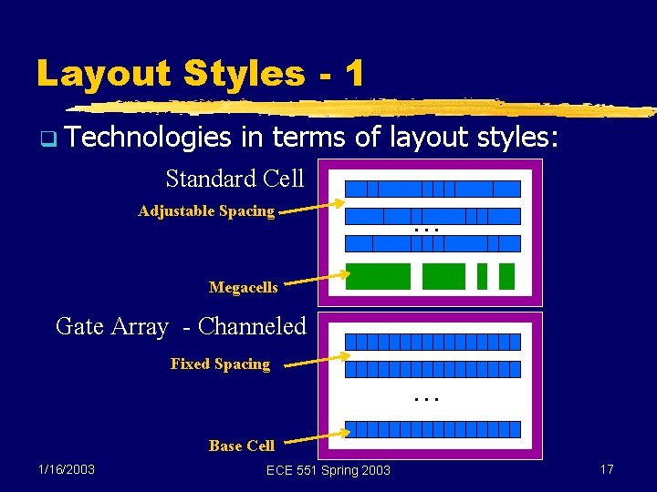
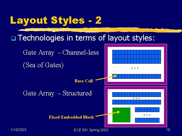
Technologies in Terms of Shared Fabrication Steps q Custom Fabricated Layers o Full Custom and Standard Cells – all layers are custom fabricated o Gate Arrays and Sea of Gates – only interconnect (metallization) layers custom fabricated o FPGAs and PLDs – nothing is custom fabricated q Consequences due to economy-of-scale: o Fab costs reduced for Gate Arrays and Sea of Gates o Fab costs further reduced for FPGAs and PLDs 1/16/2003 ECE 551 Spring 2003 16

Layout Styles - 1 q Technologies in terms of layout styles: Standard Cell Adjustable Spacing … Megacells Gate Array - Channeled Fixed Spacing … Base Cell 1/16/2003 ECE 551 Spring 2003 17

Layout Styles - 2 q Technologies in terms of layout styles: Gate Array - Channel-less … (Sea of Gates) Base Cell Gate Array - Structured Fixed Embedded Block 1/16/2003 ECE 551 Spring 2003 … … 18
![IC Costs 1 q An example 10 000 gate circuit 1 o Fixed IC Costs - 1 q An example: 10, 000 gate circuit [1] o Fixed](https://slidetodoc.com/presentation_image_h/d83ac13b4f1aff800cc9d8e2828d5a85/image-19.jpg)
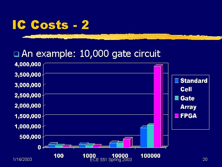
IC Costs - 1 q An example: 10, 000 gate circuit [1] o Fixed costs § Standard Cell - $146, 000 § Gate Array - $86, 000 § FPGA - $21, 800 o Variable costs § Standard Cell - $8 per IC § Gate Array - $10 per IC § FPGA - $39 per IC 1/16/2003 ECE 551 Spring 2003 19

IC Costs - 2 q An 1/16/2003 example: 10, 000 gate circuit ECE 551 Spring 2003 20

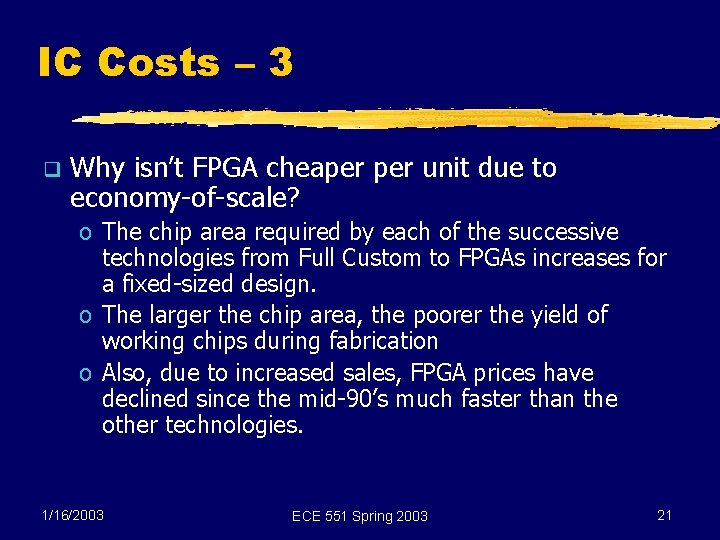
IC Costs – 3 q Why isn’t FPGA cheaper unit due to economy-of-scale? o The chip area required by each of the successive technologies from Full Custom to FPGAs increases for a fixed-sized design. o The larger the chip area, the poorer the yield of working chips during fabrication o Also, due to increased sales, FPGA prices have declined since the mid-90’s much faster than the other technologies. 1/16/2003 ECE 551 Spring 2003 21

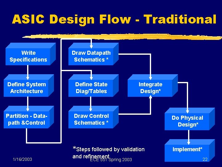
ASIC Design Flow - Traditional Write Specifications Draw Datapath Schematics * Define System Architecture Define State Diag/Tables Partition - Datapath &Control Draw Control Schematics * Do Physical Design* *Steps followed by validation Implement* 1/16/2003 and refinement ECE 551 Spring 2003 Integrate Design* 22

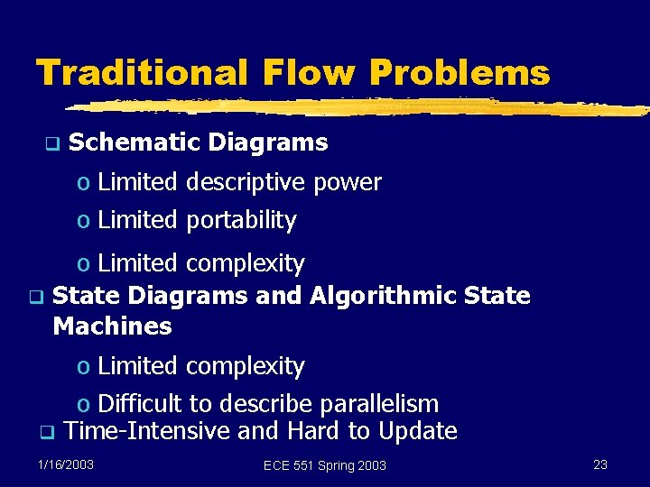
Traditional Flow Problems q Schematic Diagrams o Limited descriptive power o Limited portability o Limited complexity q State Diagrams and Algorithmic State Machines o Limited complexity o Difficult to describe parallelism q Time-Intensive and Hard to Update 1/16/2003 ECE 551 Spring 2003 23

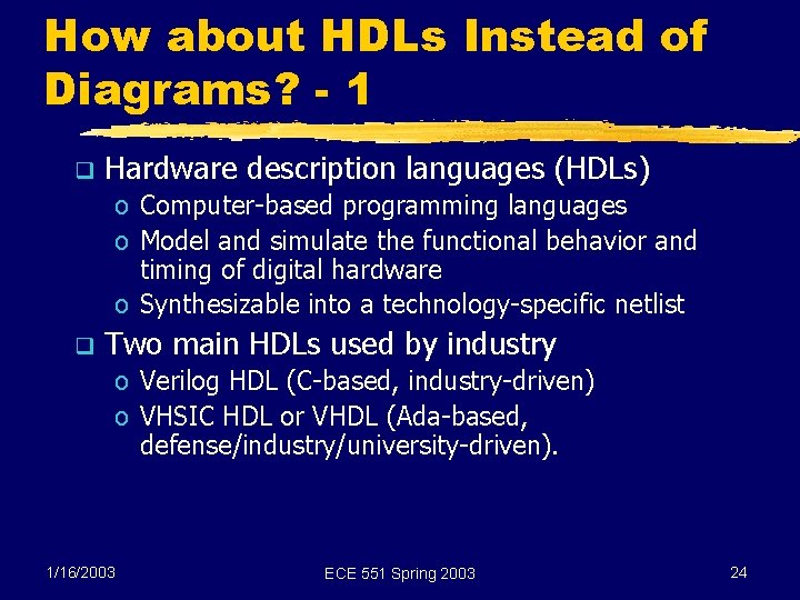
How about HDLs Instead of Diagrams? - 1 q Hardware description languages (HDLs) o Computer-based programming languages o Model and simulate the functional behavior and timing of digital hardware o Synthesizable into a technology-specific netlist q Two main HDLs used by industry o Verilog HDL (C-based, industry-driven) o VHSIC HDL or VHDL (Ada-based, defense/industry/university-driven). 1/16/2003 ECE 551 Spring 2003 24

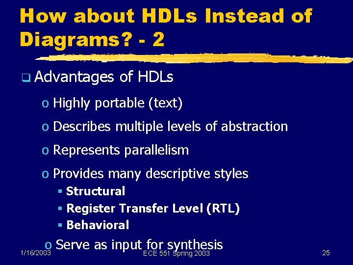
How about HDLs Instead of Diagrams? - 2 q Advantages of HDLs o Highly portable (text) o Describes multiple levels of abstraction o Represents parallelism o Provides many descriptive styles § Structural § Register Transfer Level (RTL) § Behavioral o Serve as input ECE for 551 synthesis Spring 2003 1/16/2003 25

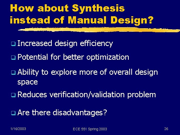
How about Synthesis instead of Manual Design? q Increased q Potential q Ability space 1/16/2003 for better optimization to explore more of overall design q Reduces q Are design efficiency verification/validation problem there disadvantages? ECE 551 Spring 2003 26

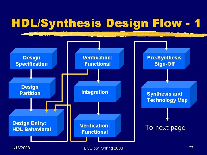
HDL/Synthesis Design Flow - 1 Design Specification Design Partition Design Entry: HDL Behavioral 1/16/2003 Verification: Functional Pre-Synthesis Sign-Off Integration Synthesis and Technology Map Verification: Functional ECE 551 Spring 2003 To next page 27

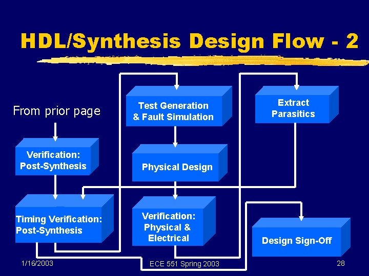
HDL/Synthesis Design Flow - 2 From prior page Verification: Post-Synthesis Timing Verification: Post-Synthesis 1/16/2003 Test Generation & Fault Simulation Extract Parasitics Physical Design Verification: Physical & Electrical ECE 551 Spring 2003 Design Sign-Off 28

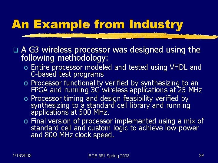
An Example from Industry q A G 3 wireless processor was designed using the following methodology: o Entire processor modeled and tested using VHDL and C-based test programs o Processor functionality verified by synthesizing to an FPGA and running 3 G wireless applications at 25 MHz o Processor timing and design feasibility verified by synthesizing to a standard cell library and running applications at 500 MHz. o Final version of processor implemented using a mix of standard cell and custom logic to achieve low-power and 800 MHz clock speed. 1/16/2003 ECE 551 Spring 2003 29

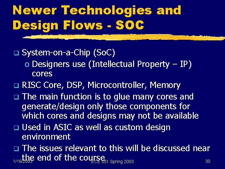
Newer Technologies and Design Flows - SOC System-on-a-Chip (So. C) o Designers use (Intellectual Property – IP) cores q RISC Core, DSP, Microcontroller, Memory q The main function is to glue many cores and generate/design only those components for which cores and designs may not be available q Used in ASIC as well as custom design environment q The issues relevant to this will be discussed near the end of the course 1/16/2003 30 ECE 551 Spring 2003 q

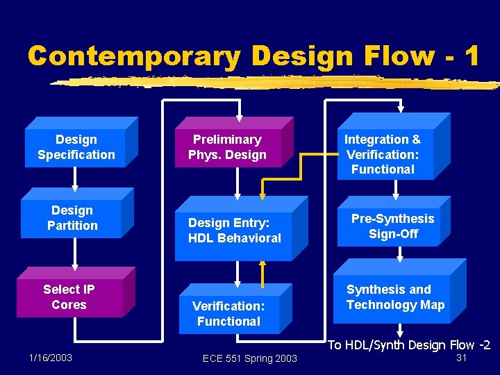
Contemporary Design Flow - 1 Design Specification Design Partition Select IP Cores 1/16/2003 Preliminary Phys. Design Entry: HDL Behavioral Verification: Functional Integration & Verification: Functional Pre-Synthesis Sign-Off Synthesis and Technology Map To HDL/Synth Design Flow -2 ECE 551 Spring 2003 31

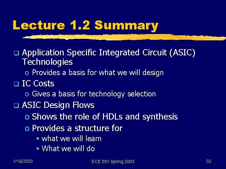
Lecture 1. 2 Summary q Application Specific Integrated Circuit (ASIC) Technologies o Provides a basis for what we will design q IC Costs o Gives a basis for technology selection q ASIC Design Flows o Shows the role of HDLs and synthesis o Provides a structure for § what we will learn § What we will do 1/16/2003 ECE 551 Spring 2003 32

References 1) Smith, Michael J. S. , Application. Specific Integrated Circuits, Addison. Wesley, 1997. 1/16/2003 ECE 551 Spring 2003 33

Lecture 1. 3 Pragmatics 1 q Pragmatics refers to practical design choices and techniques q Topics o Cell Libraries o Asynchronous Circuits o Three-State Logic and Hi-Z State 1/16/2003 ECE 551 Spring 2003 34

Cells and Cell Libraries q What is a cell? q What is a cell library? q What appears in the cell library for each ASIC cell? 1/16/2003 ECE 551 Spring 2003 35

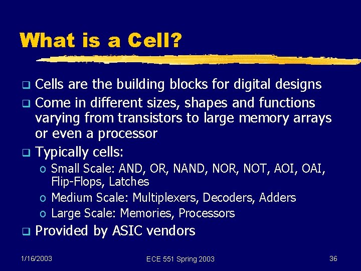
What is a Cell? Cells are the building blocks for digital designs q Come in different sizes, shapes and functions varying from transistors to large memory arrays or even a processor q Typically cells: q o Small Scale: AND, OR, NAND, NOR, NOT, AOI, OAI, Flip-Flops, Latches o Medium Scale: Multiplexers, Decoders, Adders o Large Scale: Memories, Processors q Provided by ASIC vendors 1/16/2003 ECE 551 Spring 2003 36

What is a Cell Library? q. A database specifying and describing the target technology in the form of predesigned objects called cells. Synthesis target technology. q In-Class Discussion: What are typical components in the database for each cell? 1/16/2003 ECE 551 Spring 2003 37

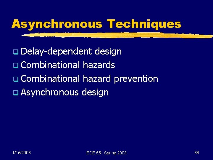
Asynchronous Techniques q Delay-dependent design q Combinational hazards q Combinational hazard prevention q Asynchronous design 1/16/2003 ECE 551 Spring 2003 38

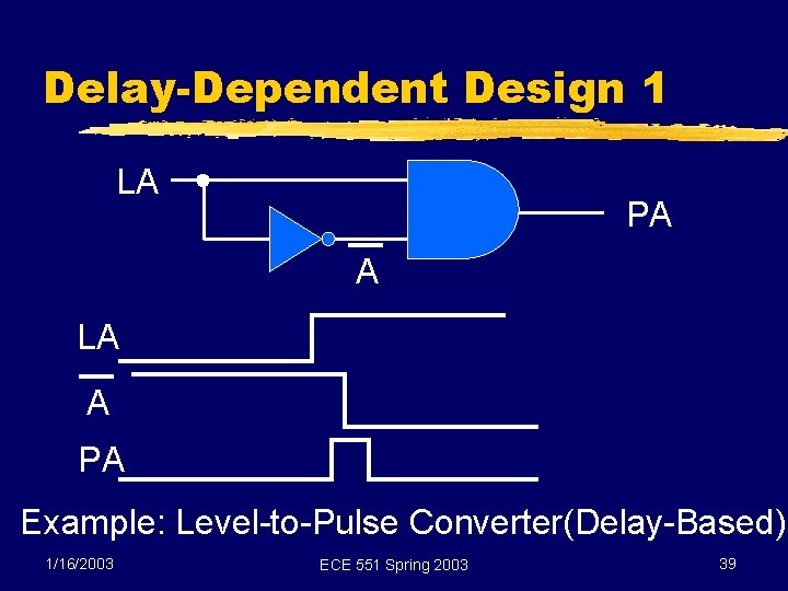
Delay-Dependent Design 1 LA PA A LA A PA Example: Level-to-Pulse Converter(Delay-Based) 1/16/2003 ECE 551 Spring 2003 39

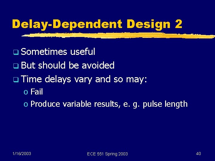
Delay-Dependent Design 2 q Sometimes useful q But should be avoided q Time delays vary and so may: o Fail o Produce variable results, e. g. pulse length 1/16/2003 ECE 551 Spring 2003 40

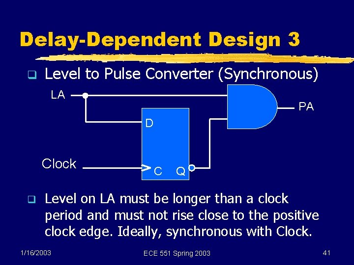
Delay-Dependent Design 3 q Level to Pulse Converter (Synchronous) LA PA D Clock q C Q Level on LA must be longer than a clock period and must not rise close to the positive clock edge. Ideally, synchronous with Clock. 1/16/2003 ECE 551 Spring 2003 41

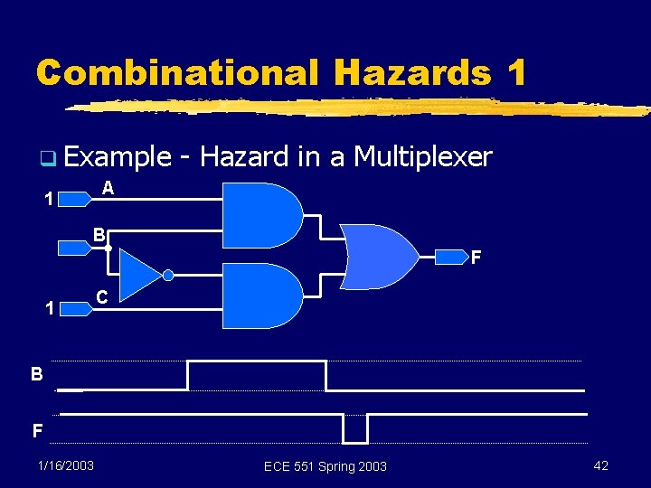
Combinational Hazards 1 q Example - Hazard in a Multiplexer A 1 B F 1 C B F 1/16/2003 ECE 551 Spring 2003 42

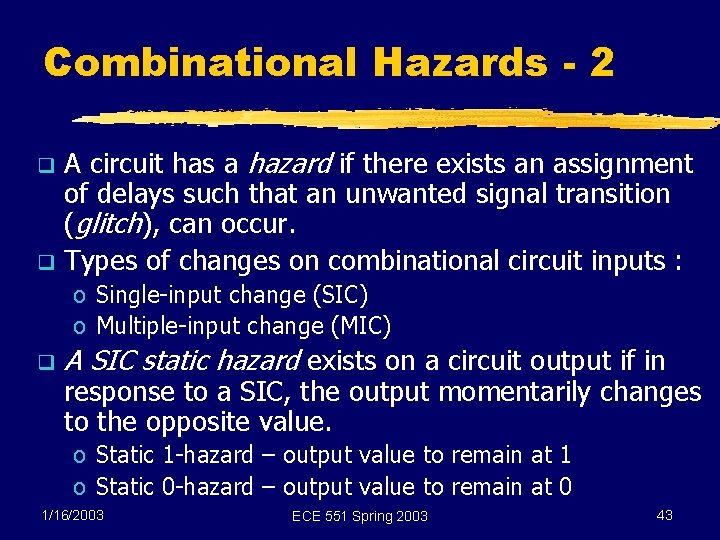
Combinational Hazards - 2 A circuit has a hazard if there exists an assignment of delays such that an unwanted signal transition (glitch), can occur. q Types of changes on combinational circuit inputs : q o Single-input change (SIC) o Multiple-input change (MIC) q A SIC static hazard exists on a circuit output if in response to a SIC, the output momentarily changes to the opposite value. o Static 1 -hazard – output value to remain at 1 o Static 0 -hazard – output value to remain at 0 1/16/2003 ECE 551 Spring 2003 43

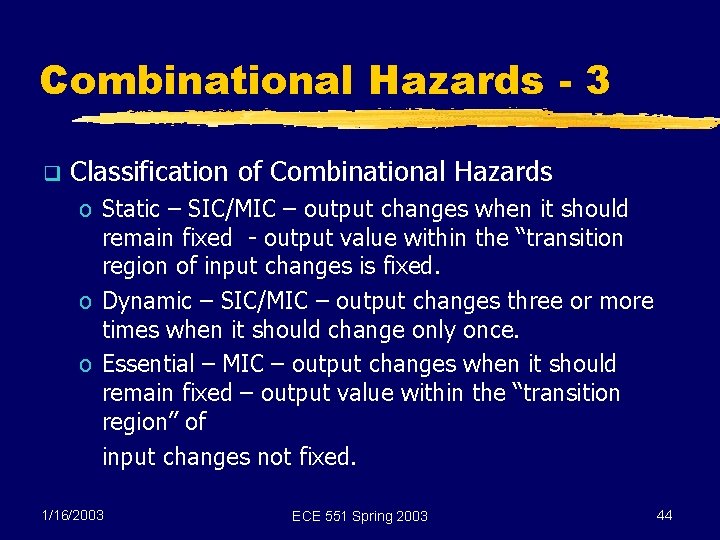
Combinational Hazards - 3 q Classification of Combinational Hazards o Static – SIC/MIC – output changes when it should remain fixed - output value within the “transition region of input changes is fixed. o Dynamic – SIC/MIC – output changes three or more times when it should change only once. o Essential – MIC – output changes when it should remain fixed – output value within the “transition region” of input changes not fixed. 1/16/2003 ECE 551 Spring 2003 44

Combination Hazards - 4 q In-class Example: Illustration of static, dynamic and essential hazards 1/16/2003 ECE 551 Spring 2003 45

Combinational Hazards - 5 q Consequences of Hazards o Signals with hazards within or entering asynchronous circuits (note that a flip-flop is an asynchronous circuit with respect to its clock signal!) o Cause incorrect state behavior § Extra state changes § Incorrect state changes q In-Class Example: Prevention of Hazards o Redundant Logic o Delay Dependence 1/16/2003 ECE 551 Spring 2003 46

Asynchronous Design - 1 q Which of the following sequential circuits involve asynchronous design? o A circuit that has no global clock signal involved in its operation – state changes occur in response to input changes only. o A D flip-flop circuit o A circuit using clock gating on flip-flop clock inputs o A circuit with a clock which uses the clear and preset inputs on the flip-flops for other than initialization. 1/16/2003 ECE 551 Spring 2003 47

Asynchronous Design - 2 Because of the difficulty of eliminating hazards, it is very difficult to insure correct operation under all timing possibilities q Design must be done manually or by use of very specialized synthesis tools. q Therefore, avoid it if you can! q If you truly need it, investigate some of the more contemporary approaches[1] which avoid some of the many difficulties. q 1/16/2003 ECE 551 Spring 2003 48

Three-State and Other Hi-Z States Three-state conflicts q Floating three-state nets and inputs q Pull-ups and Pull-downs q Bus keepers q 1/16/2003 ECE 551 Spring 2003 49

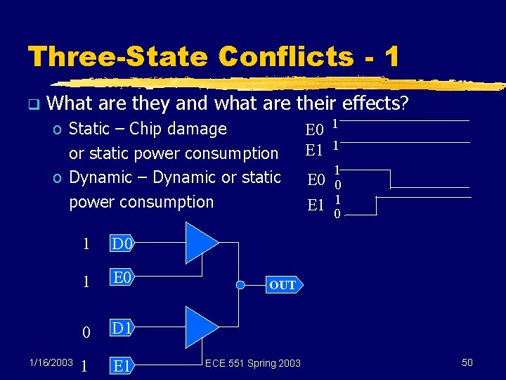
Three-State Conflicts - 1 q What are they and what are their effects? o Static – Chip damage or static power consumption o Dynamic – Dynamic or static power consumption 1/16/2003 1 D 0 1 E 0 0 D 1 1 E 0 1 E 1 1 E 0 E 1 1 0 OUT ECE 551 Spring 2003 50

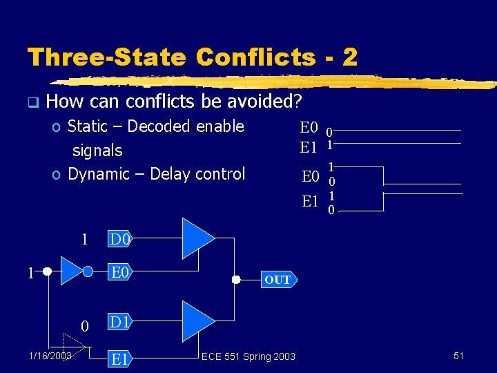
Three-State Conflicts - 2 q How can conflicts be avoided? o Static – Decoded enable signals o Dynamic – Delay control 1 0 1/16/2003 E 0 E 1 1 0 D 0 E 0 1 E 0 0 E 1 1 OUT D 1 ECE 551 Spring 2003 51

Floating Inputs and Three. State Nets - 1 q Floating input values on gates can cause: o static power dissipation o high-frequency switching that induces power supply noise q Floating input values arise from: o Gate inputs, e. g. , for example on exterior of IC, that are not connected o Lines driven by 3 -state buffer or gate outputs, all of which are in the Hi-Z state. 1/16/2003 ECE 551 Spring 2003 52

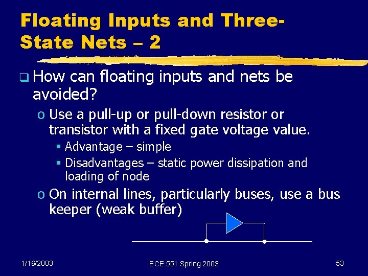
Floating Inputs and Three. State Nets – 2 q How can floating inputs and nets be avoided? o Use a pull-up or pull-down resistor or transistor with a fixed gate voltage value. § Advantage – simple § Disadvantages – static power dissipation and loading of node o On internal lines, particularly buses, use a bus keeper (weak buffer) 1/16/2003 ECE 551 Spring 2003 53

Non-D flip-flops q D Flip-Flops o Unique characteristic – the typical master-slave DFF is also functionally an edge-triggered DFF. q Non- D Flip-Flops (JK, T, etc. ) o In the cell libraries, these flip-flop may be full-custom designs or may simply consist of a DFF with added logic. o If it is just a DFF with added logic, you might as well design for a DFF to give the logic optimization software more flexibility. 1/16/2003 ECE 551 Spring 2003 54
![References 1 Chris J Myers Asynchronous Circuit Design John Wiley Sons Inc References [1] Chris J. Myers, Asynchronous Circuit Design, John Wiley & Sons, Inc. ,](https://slidetodoc.com/presentation_image_h/d83ac13b4f1aff800cc9d8e2828d5a85/image-55.jpg)
References [1] Chris J. Myers, Asynchronous Circuit Design, John Wiley & Sons, Inc. , New York, 2001. 1/16/2003 ECE 551 Spring 2003 55