Contents Introduction n Computer Architecture n ARM Architecture

![Levels of Abstraction temp = v[k]; High Level Language Program (e. g. , C) Levels of Abstraction temp = v[k]; High Level Language Program (e. g. , C)](https://slidetodoc.com/presentation_image/1e65fa8916ef61147f3aee0113ef3149/image-15.jpg)


- Slides: 67


Contents Introduction n Computer Architecture n ARM Architecture n Development Tools : GNU Development Tools n ARM Instruction Set n ARM Assembly Language n ARM Assembly Programming : GNU ARM Tool. Chain n Interrupts and Monitor n 2

Lecture 2 Computer Architecture

Outline n n n Basic Concepts Instruction Set Architecture Machine Organization 4

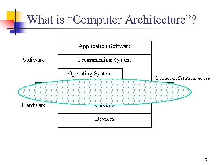
What is “Computer Architecture”? Application Software Programming System Operating System Processor Hardware Memory Instruction Set Architecture I/O System Circuits Devices 5

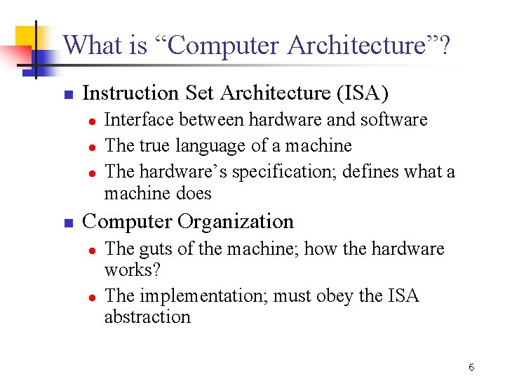
What is “Computer Architecture”? n Instruction Set Architecture (ISA) l l l n Interface between hardware and software The true language of a machine The hardware’s specification; defines what a machine does Computer Organization l l The guts of the machine; how the hardware works? The implementation; must obey the ISA abstraction 6

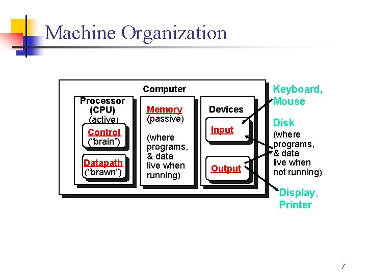
Machine Organization Computer Processor (CPU) (active) Control (“brain”) Datapath (“brawn”) Memory (passive) (where programs, & data live when running) Devices Input Output Keyboard, Mouse Disk (where programs, & data live when not running) Display, Printer 7

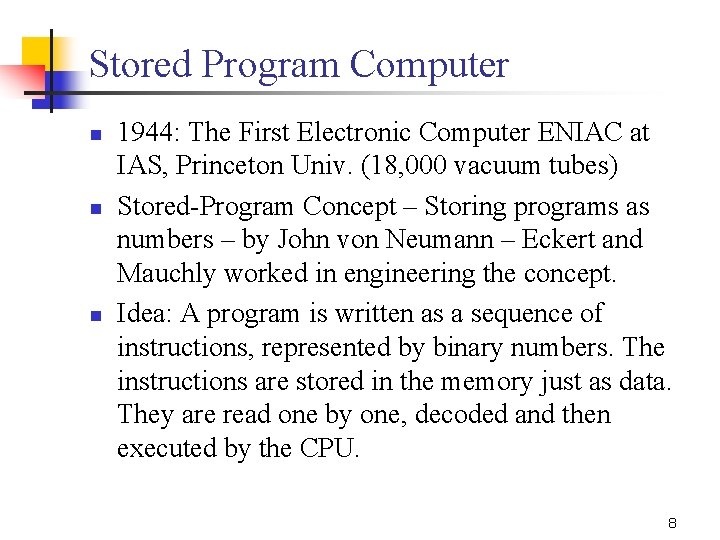
Stored Program Computer n n n 1944: The First Electronic Computer ENIAC at IAS, Princeton Univ. (18, 000 vacuum tubes) Stored-Program Concept – Storing programs as numbers – by John von Neumann – Eckert and Mauchly worked in engineering the concept. Idea: A program is written as a sequence of instructions, represented by binary numbers. The instructions are stored in the memory just as data. They are read one by one, decoded and then executed by the CPU. 8

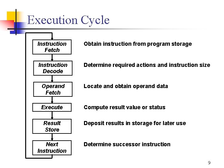
Execution Cycle Instruction Fetch Obtain instruction from program storage Instruction Decode Determine required actions and instruction size Operand Fetch Locate and obtain operand data Execute Compute result value or status Result Store Next Instruction Deposit results in storage for later use Determine successor instruction 9

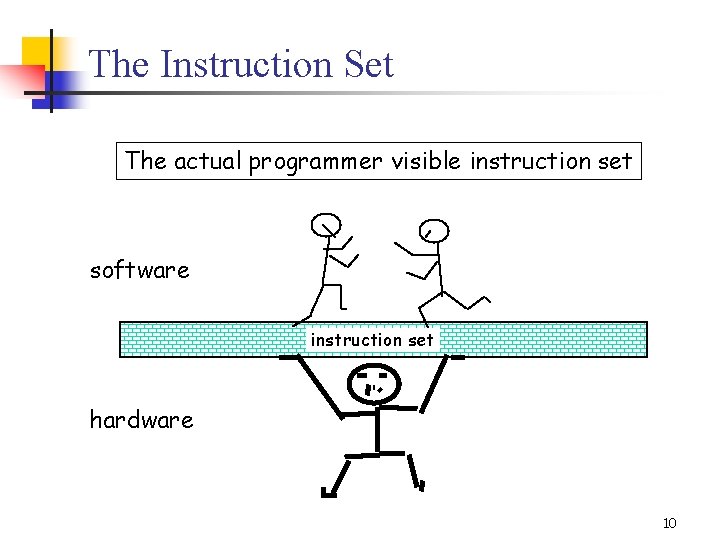
The Instruction Set The actual programmer visible instruction set software instruction set hardware 10

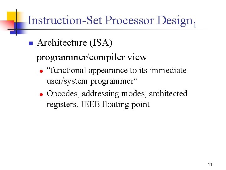
Instruction-Set Processor Design 1 n Architecture (ISA) programmer/compiler view l l “functional appearance to its immediate user/system programmer” Opcodes, addressing modes, architected registers, IEEE floating point 11

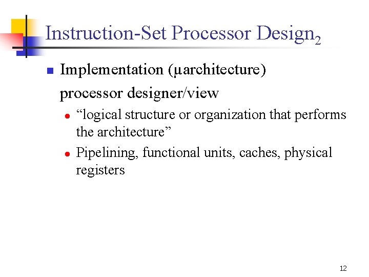
Instruction-Set Processor Design 2 n Implementation (µarchitecture) processor designer/view l l “logical structure or organization that performs the architecture” Pipelining, functional units, caches, physical registers 12

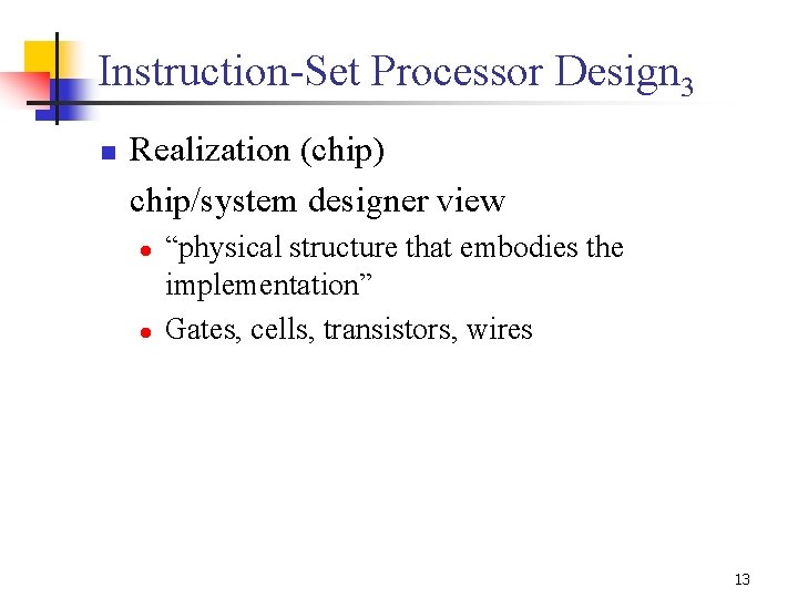
Instruction-Set Processor Design 3 n Realization (chip) chip/system designer view l l “physical structure that embodies the implementation” Gates, cells, transistors, wires 13

Outline n n n Basic Concepts Instruction Set Architecture Machine Organization 14
![Levels of Abstraction temp vk High Level Language Program e g C Levels of Abstraction temp = v[k]; High Level Language Program (e. g. , C)](https://slidetodoc.com/presentation_image/1e65fa8916ef61147f3aee0113ef3149/image-15.jpg)
Levels of Abstraction temp = v[k]; High Level Language Program (e. g. , C) v[k] = v[k+1]; v[k+1] = temp; Compiler lw lw sw sw Assembly Language Program (e. g. , MIPS) Assembler Machine Language Program (MIPS) 0000 1010 1100 0101 1001 1111 0110 1000 $15, $16, $15, 1100 0101 1010 0000 0110 1000 1111 1001 0($2) 4($2) 1010 0000 0101 1100 1111 1000 0110 0101 1100 0000 1010 1000 0110 1001 1111 Machine Interpretation Datapath Transfer Specification ° ° IR <- Imem[PC]; PC <- PC + 4 15

Recall in C language n n Operators: +, -, *, /, % Operands: l l n Variables Constants Assignment statement: variable = expression l Expressions consist of operators operating on operands 16

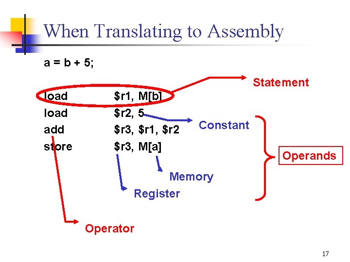
When Translating to Assembly a = b + 5; Statement load add store $r 1, M[b] $r 2, 5 $r 3, $r 1, $r 2 $r 3, M[a] Constant Operands Memory Register Operator 17

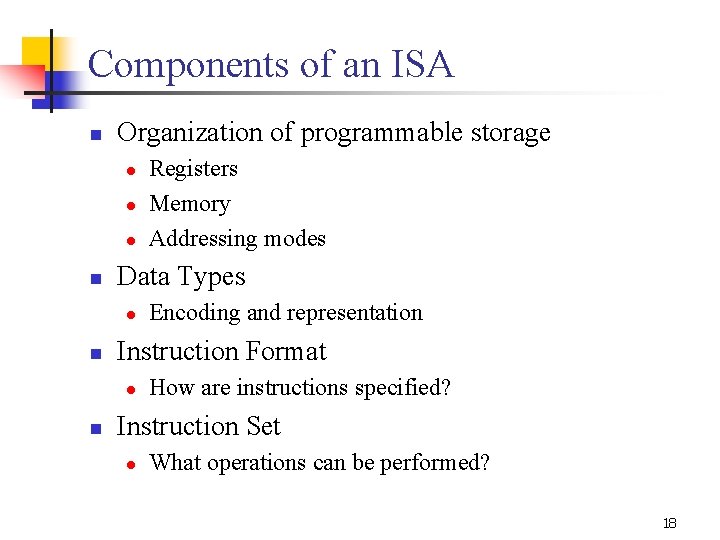
Components of an ISA n Organization of programmable storage l l l n Data Types l n Encoding and representation Instruction Format l n Registers Memory Addressing modes How are instructions specified? Instruction Set l What operations can be performed? 18

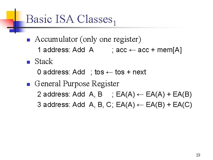
Basic ISA Classes 1 n Accumulator (only one register) 1 address: Add A n ; acc ← acc + mem[A] Stack 0 address: Add ; tos ← tos + next n General Purpose Register 2 address: Add A, B ; EA(A) ← EA(A) + EA(B) 3 address: Add A, B, C; EA(A) ← EA(B) + EA(C) 19

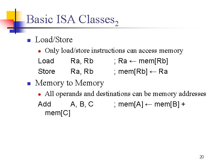
Basic ISA Classes 2 n Load/Store Only load/store instructions can access memory Load Ra, Rb ; Ra ← mem[Rb] Store Ra, Rb ; mem[Rb] ← Ra l n Memory to Memory All operands and destinations can be memory addresses Add A, B, C ; mem[A] ← mem[B] + mem[C] l 20

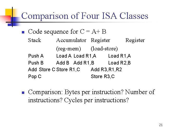
Comparison of Four ISA Classes n Code sequence for C = A+ B Stack Accumulator Register (reg-mem) (load-store) Register Push A Load R 1, A Push B Add R 1, B Load R 2, B Add Store C Store R 1, C Add R 3, R 1, R 2 Pop C Store R 3, C n Comparison: Bytes per instruction? Number of instructions? Cycles per instructions? 21

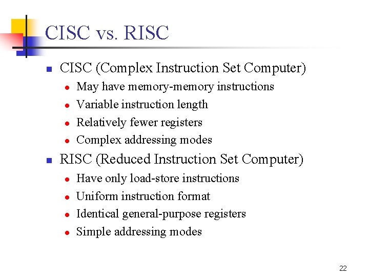
CISC vs. RISC n CISC (Complex Instruction Set Computer) l l n May have memory-memory instructions Variable instruction length Relatively fewer registers Complex addressing modes RISC (Reduced Instruction Set Computer) l l Have only load-store instructions Uniform instruction format Identical general-purpose registers Simple addressing modes 22

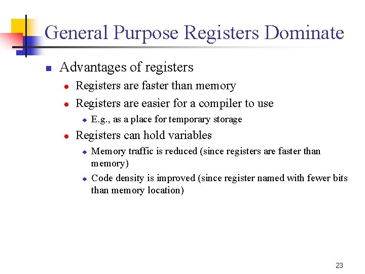
General Purpose Registers Dominate n Advantages of registers l l Registers are faster than memory Registers are easier for a compiler to use u l E. g. , as a place for temporary storage Registers can hold variables u u Memory traffic is reduced (since registers are faster than memory) Code density is improved (since register named with fewer bits than memory location) 23

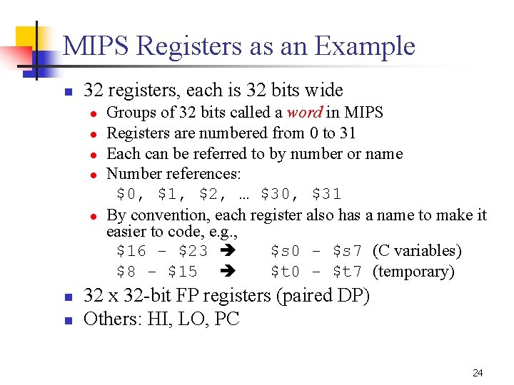
MIPS Registers as an Example n 32 registers, each is 32 bits wide l l l n n Groups of 32 bits called a word in MIPS Registers are numbered from 0 to 31 Each can be referred to by number or name Number references: $0, $1, $2, … $30, $31 By convention, each register also has a name to make it easier to code, e. g. , $16 - $23 $s 0 - $s 7 (C variables) $8 - $15 $t 0 - $t 7 (temporary) 32 x 32 -bit FP registers (paired DP) Others: HI, LO, PC 24

Memory Addressing n n Since 1980 almost every machine uses addresses to level of 8 -bits (byte) 2 questions for the design of ISA l l Read a 32 -bit word as four loads of bytes from sequential byte addresses or as one load word from a single byte address? Can a word be place on any byte-boundary? 25

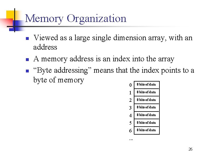
Memory Organization n Viewed as a large single dimension array, with an address A memory address is an index into the array “Byte addressing” means that the index points to a byte of memory 8 bits of data 0 1 2 3 4 5 6. . . 8 bits of data 8 bits of data 26

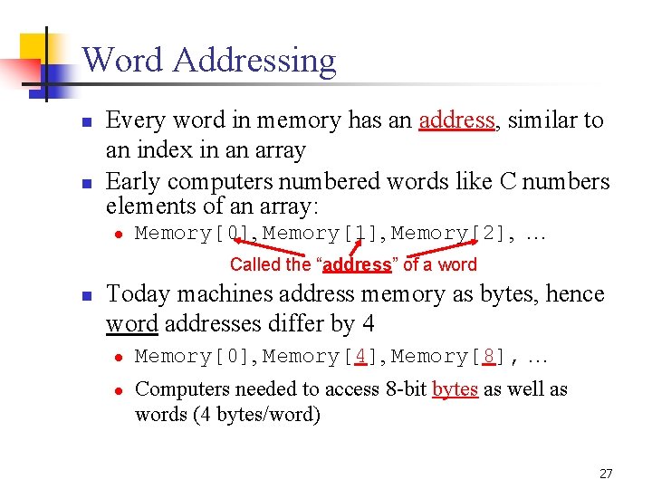
Word Addressing n n Every word in memory has an address, similar to an index in an array Early computers numbered words like C numbers elements of an array: l Memory[0], Memory[1], Memory[2], … Called the “address” of a word n Today machines address memory as bytes, hence word addresses differ by 4 l l Memory[0], Memory[4], Memory[8], … Computers needed to access 8 -bit bytes as well as words (4 bytes/word) 27

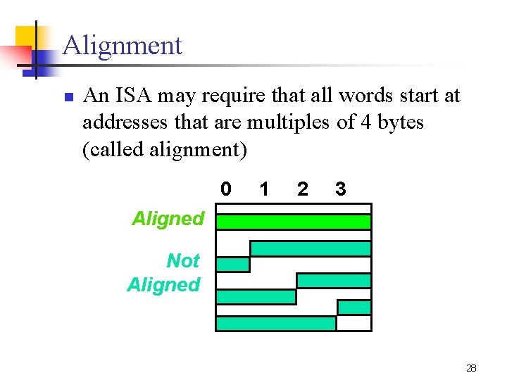
Alignment n An ISA may require that all words start at addresses that are multiples of 4 bytes (called alignment) 0 1 2 3 Aligned Not Aligned 28

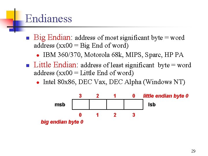
Endianess n Big Endian: address of most significant byte = word address (xx 00 = Big End of word) l IBM 360/370, Motorola 68 k, MIPS, Sparc, HP PA n Little Endian: address of least significant byte = word address (xx 00 = Little End of word) l Intel 80 x 86, DEC Vax, DEC Alpha (Windows NT) 3 2 1 0 msb 0 big endian byte 0 little endian byte 0 lsb 1 2 3 29

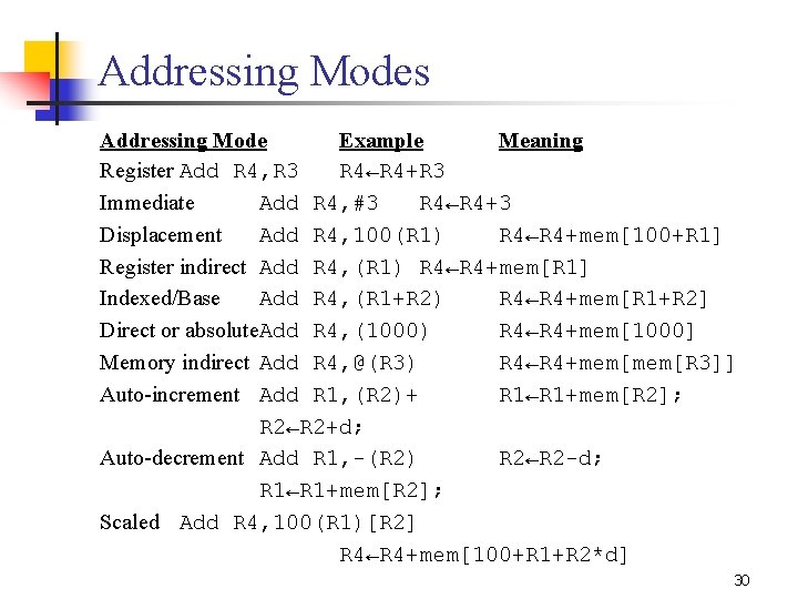
Addressing Modes Addressing Mode Example Meaning Register Add R 4, R 3 R 4←R 4+R 3 Immediate Add R 4, #3 R 4←R 4+3 Displacement Add R 4, 100(R 1) R 4←R 4+mem[100+R 1] Register indirect Add R 4, (R 1) R 4←R 4+mem[R 1] Indexed/Base Add R 4, (R 1+R 2) R 4←R 4+mem[R 1+R 2] Direct or absolute. Add R 4, (1000) R 4←R 4+mem[1000] Memory indirect Add R 4, @(R 3) R 4←R 4+mem[R 3]] Auto-increment Add R 1, (R 2)+ R 1←R 1+mem[R 2]; R 2←R 2+d; Auto-decrement Add R 1, -(R 2) R 2←R 2 -d; R 1←R 1+mem[R 2]; Scaled Add R 4, 100(R 1)[R 2] R 4←R 4+mem[100+R 1+R 2*d] 30

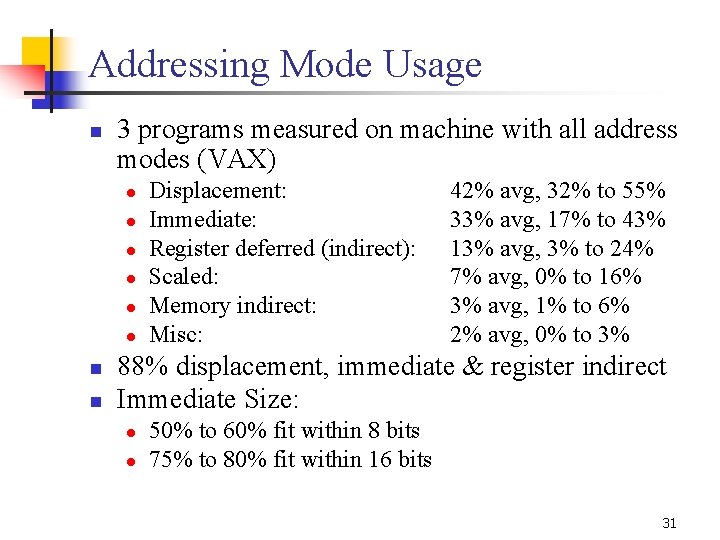
Addressing Mode Usage n 3 programs measured on machine with all address modes (VAX) l l l n n Displacement: Immediate: Register deferred (indirect): Scaled: Memory indirect: Misc: 42% avg, 32% to 55% 33% avg, 17% to 43% 13% avg, 3% to 24% 7% avg, 0% to 16% 3% avg, 1% to 6% 2% avg, 0% to 3% 88% displacement, immediate & register indirect Immediate Size: l l 50% to 60% fit within 8 bits 75% to 80% fit within 16 bits 31

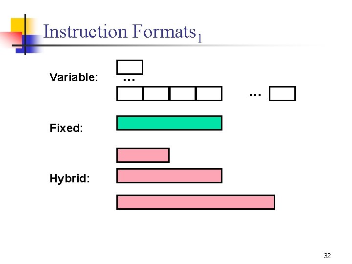
Instruction Formats 1 Variable: … … Fixed: Hybrid: 32

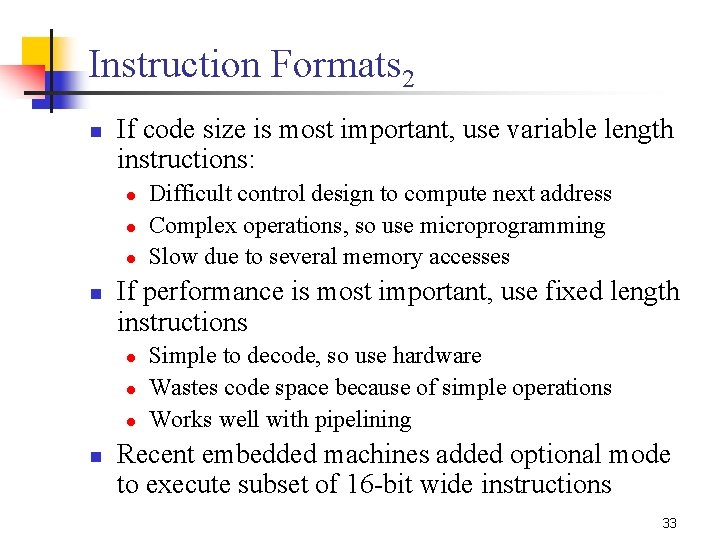
Instruction Formats 2 n If code size is most important, use variable length instructions: l l l n If performance is most important, use fixed length instructions l l l n Difficult control design to compute next address Complex operations, so use microprogramming Slow due to several memory accesses Simple to decode, so use hardware Wastes code space because of simple operations Works well with pipelining Recent embedded machines added optional mode to execute subset of 16 -bit wide instructions 33

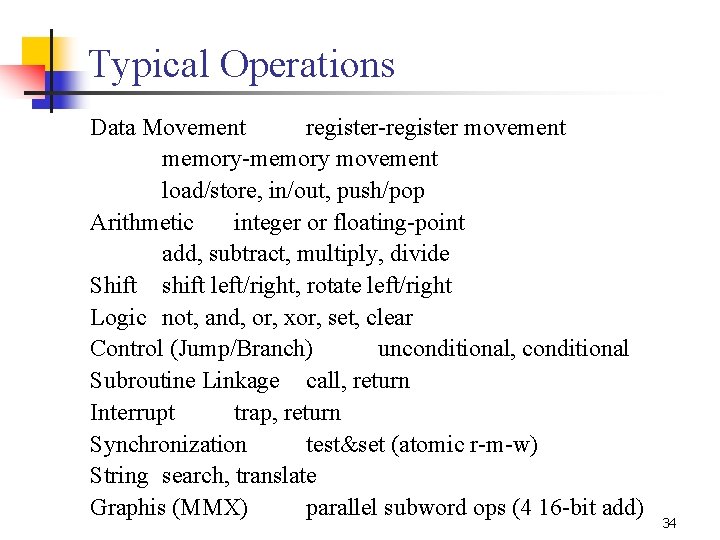
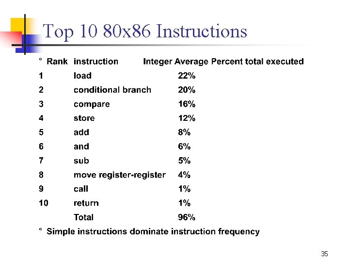
Typical Operations Data Movement register-register movement memory-memory movement load/store, in/out, push/pop Arithmetic integer or floating-point add, subtract, multiply, divide Shift shift left/right, rotate left/right Logic not, and, or, xor, set, clear Control (Jump/Branch) unconditional, conditional Subroutine Linkage call, return Interrupt trap, return Synchronization test&set (atomic r-m-w) String search, translate Graphis (MMX) parallel subword ops (4 16 -bit add) 34

Top 10 80 x 86 Instructions 35

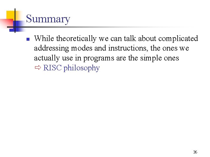
Summary n While theoretically we can talk about complicated addressing modes and instructions, the ones we actually use in programs are the simple ones RISC philosophy 36

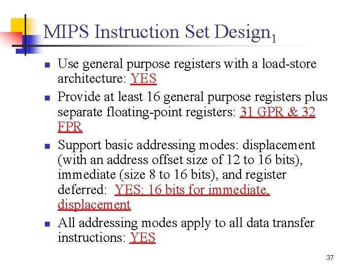
MIPS Instruction Set Design 1 n n Use general purpose registers with a load-store architecture: YES Provide at least 16 general purpose registers plus separate floating-point registers: 31 GPR & 32 FPR Support basic addressing modes: displacement (with an address offset size of 12 to 16 bits), immediate (size 8 to 16 bits), and register deferred: YES: 16 bits for immediate, displacement All addressing modes apply to all data transfer instructions: YES 37

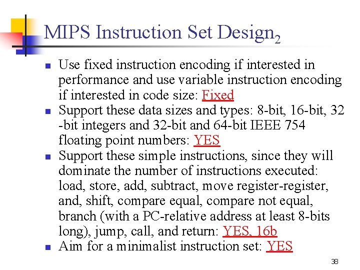
MIPS Instruction Set Design 2 n n Use fixed instruction encoding if interested in performance and use variable instruction encoding if interested in code size: Fixed Support these data sizes and types: 8 -bit, 16 -bit, 32 -bit integers and 32 -bit and 64 -bit IEEE 754 floating point numbers: YES Support these simple instructions, since they will dominate the number of instructions executed: load, store, add, subtract, move register-register, and, shift, compare equal, compare not equal, branch (with a PC-relative address at least 8 -bits long), jump, call, and return: YES, 16 b Aim for a minimalist instruction set: YES 38

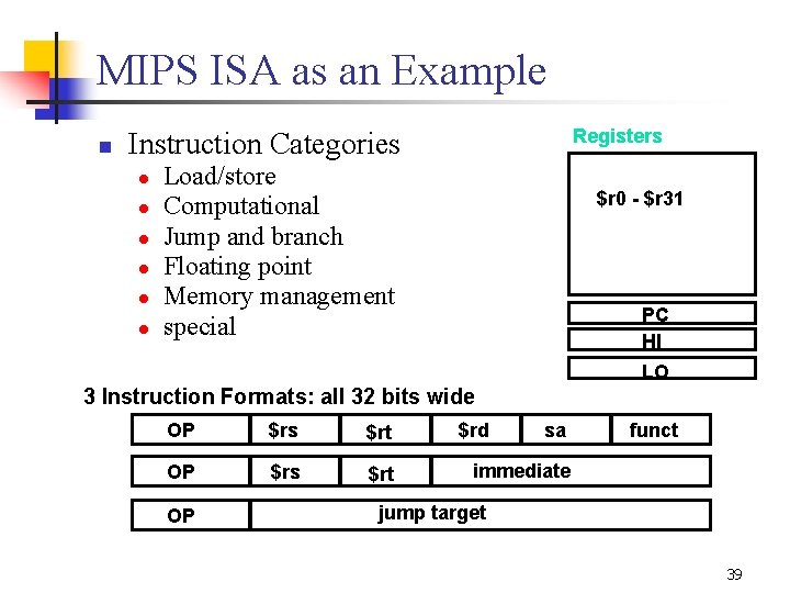
MIPS ISA as an Example n Registers Instruction Categories l l l Load/store Computational Jump and branch Floating point Memory management special $r 0 - $r 31 PC HI LO 3 Instruction Formats: all 32 bits wide OP $rs $rt OP $rd sa funct immediate jump target 39

Outline n n n Basic Concepts Instruction Set Architecture Machine Organization 40

Machine Organization Computer Processor (CPU) (active) Control (“brain”) Datapath (“brawn”) Memory (passive) (where programs, & data live when running) Devices Input Output Keyboard, Mouse Disk (where programs, & data live when not running) Display, Printer 41

Semiconductor Memory, DRAM n Semiconductor memory began to be competitive in early 1970 s l n First commercial DRAM was Intel 1103 l l n Intel formed to exploit market for semiconductor memory 1 Kbit of storage on single chip charge on a capacitor used to hold value Semiconductor memory quickly replaced core memory in ‘ 70 s 42

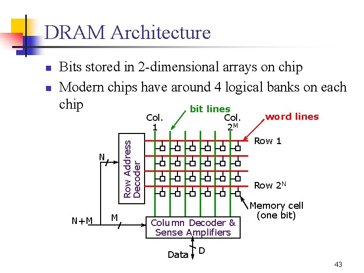
DRAM Architecture n Bits stored in 2 -dimensional arrays on chip Modern chips have around 4 logical banks on each chip bit lines Col. 1 N N+M Col. 2 M M word lines Row 1 Row Address Decoder n Row 2 N Column Decoder & Sense Amplifiers Data Memory cell (one bit) D 43

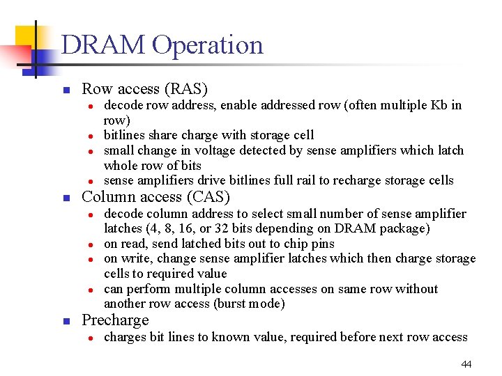
DRAM Operation n Row access (RAS) l l n Column access (CAS) l l n decode row address, enable addressed row (often multiple Kb in row) bitlines share charge with storage cell small change in voltage detected by sense amplifiers which latch whole row of bits sense amplifiers drive bitlines full rail to recharge storage cells decode column address to select small number of sense amplifier latches (4, 8, 16, or 32 bits depending on DRAM package) on read, send latched bits out to chip pins on write, change sense amplifier latches which then charge storage cells to required value can perform multiple column accesses on same row without another row access (burst mode) Precharge l charges bit lines to known value, required before next row access 44

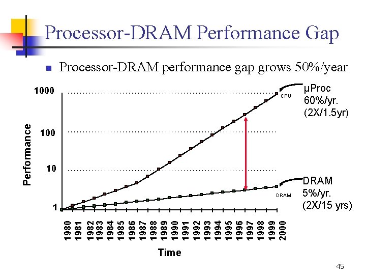
Processor-DRAM Performance Gap Processor-DRAM performance gap grows 50%/year n CPU µProc 60%/yr. (2 X/1. 5 yr) 100 10 DRAM 1 DRAM 5%/yr. (2 X/15 yrs) 1980 1981 1982 1983 1984 1985 1986 1987 1988 1989 1990 1991 1992 1993 1994 1995 1996 1997 1998 1999 2000 Performance 1000 Time 45

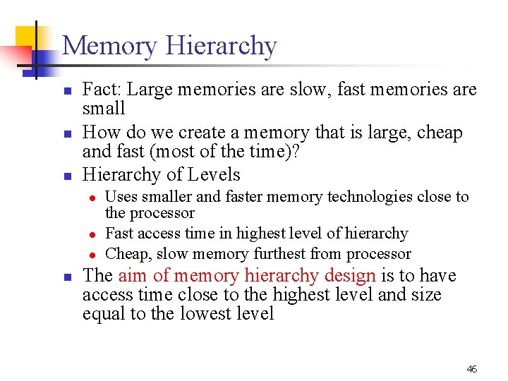
Memory Hierarchy n n n Fact: Large memories are slow, fast memories are small How do we create a memory that is large, cheap and fast (most of the time)? Hierarchy of Levels l l l n Uses smaller and faster memory technologies close to the processor Fast access time in highest level of hierarchy Cheap, slow memory furthest from processor The aim of memory hierarchy design is to have access time close to the highest level and size equal to the lowest level 46

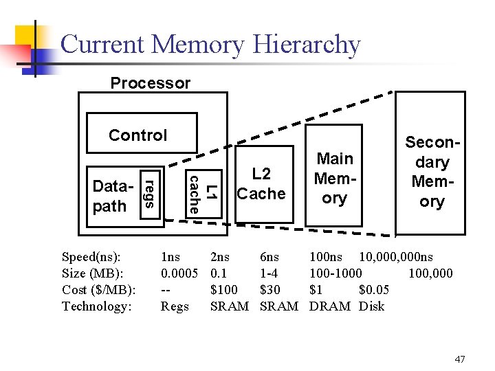
Current Memory Hierarchy Processor Control L 1 cache Speed(ns): Size (MB): Cost ($/MB): Technology: regs Datapath 1 ns 0. 0005 -Regs L 2 Cache 2 ns 0. 1 $100 SRAM 6 ns 1 -4 $30 SRAM Main Memory Secondary Memory 100 ns 10, 000 ns 100 -1000 100, 000 $1 $0. 05 DRAM Disk 47

Why Hierarchy works: Natural Locality n The Principle of Locality: l n Programs access a relatively small portion of the address space at any second Temporal Locality (Locality in Time) Recently accessed data tend to be referenced again soon n Spatial Locality (Locality in Space) nearby items will tend to be referenced soon 48

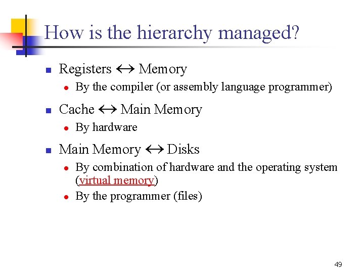
How is the hierarchy managed? n Registers « Memory l n Cache « Main Memory l n By the compiler (or assembly language programmer) By hardware Main Memory « Disks l l By combination of hardware and the operating system (virtual memory) By the programmer (files) 49

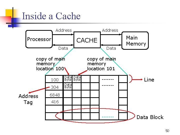
Inside a Cache Address Processor Address CACHE Data copy of main memory location 100 Address Tag 100 Data Byte 304 Data Byte Data Main Memory copy of main memory location 101 Line 6848 416 Data Block 50

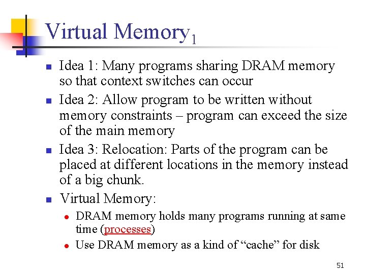
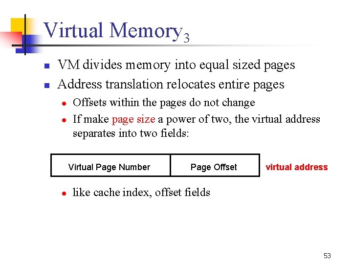
Virtual Memory 1 n n Idea 1: Many programs sharing DRAM memory so that context switches can occur Idea 2: Allow program to be written without memory constraints – program can exceed the size of the main memory Idea 3: Relocation: Parts of the program can be placed at different locations in the memory instead of a big chunk. Virtual Memory: l l DRAM memory holds many programs running at same time (processes) Use DRAM memory as a kind of “cache” for disk 51

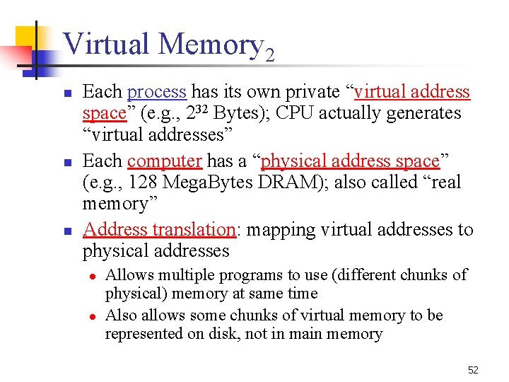
Virtual Memory 2 n n n Each process has its own private “virtual address space” (e. g. , 232 Bytes); CPU actually generates “virtual addresses” Each computer has a “physical address space” (e. g. , 128 Mega. Bytes DRAM); also called “real memory” Address translation: mapping virtual addresses to physical addresses l l Allows multiple programs to use (different chunks of physical) memory at same time Also allows some chunks of virtual memory to be represented on disk, not in main memory 52

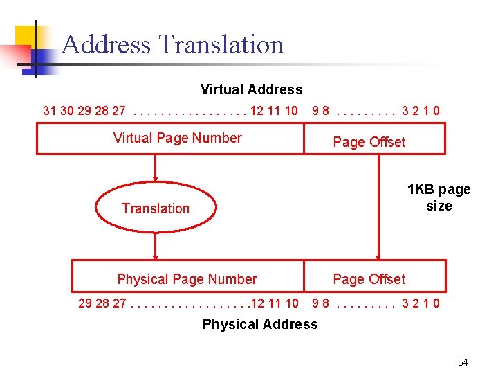
Virtual Memory 3 n n VM divides memory into equal sized pages Address translation relocates entire pages l l Offsets within the pages do not change If make page size a power of two, the virtual address separates into two fields: Virtual Page Number l Page Offset virtual address like cache index, offset fields 53

Address Translation Virtual Address 31 30 29 28 27. . . . 12 11 10 98. . 3210 Virtual Page Number Page Offset 1 KB page size Translation Physical Page Number 29 28 27. . . . 12 11 10 Page Offset 98. . 3210 Physical Address 54

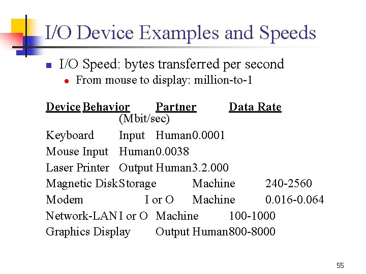
I/O Device Examples and Speeds n I/O Speed: bytes transferred per second l From mouse to display: million-to-1 Device Behavior Partner Data Rate (Mbit/sec) Keyboard Input Human 0. 0001 Mouse Input Human 0. 0038 Laser Printer Output Human 3. 2. 000 Magnetic Disk. Storage Machine 240 -2560 Modem I or O Machine 0. 016 -0. 064 Network-LAN I or O Machine 100 -1000 Graphics Display Output Human 800 -8000 55

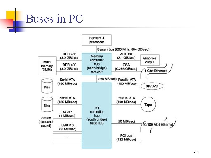
Buses in PC 56

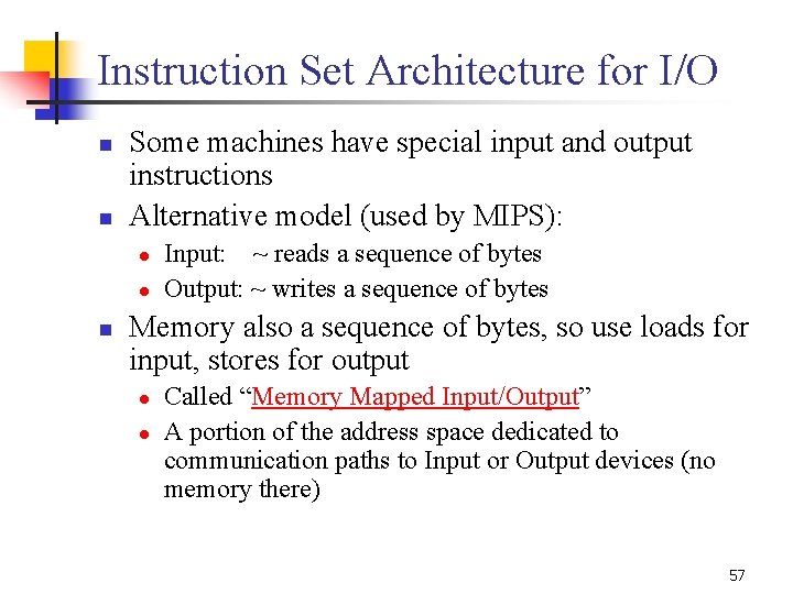
Instruction Set Architecture for I/O n n Some machines have special input and output instructions Alternative model (used by MIPS): l l n Input: ~ reads a sequence of bytes Output: ~ writes a sequence of bytes Memory also a sequence of bytes, so use loads for input, stores for output l l Called “Memory Mapped Input/Output” A portion of the address space dedicated to communication paths to Input or Output devices (no memory there) 57

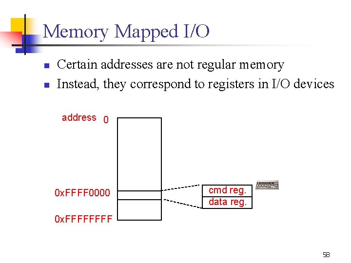
Memory Mapped I/O n n Certain addresses are not regular memory Instead, they correspond to registers in I/O devices address 0 0 x. FFFF 0000 cmd reg. data reg. 0 x. FFFF 58

Processor-I/O Speed Mismatch n 500 MHz microprocessor can execute 500 million load or store instructions per second, or 2, 000 KB/s data rate l n Input: device may not be ready to send data as fast as the processor loads it l n n I/O devices from 0. 01 KB/s to 30, 000 KB/s Also, might be waiting for human to act Output: device may not be ready to accept data as fast as processor stores it What to do? 59

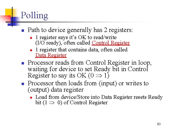
Polling n Path to device generally has 2 registers: l l n n 1 register says it’s OK to read/write (I/O ready), often called Control Register 1 register that contains data, often called Data Register Processor reads from Control Register in loop, waiting for device to set Ready bit in Control Register to say its OK (0 1) Processor then loads from (input) or writes to (output) data register l Load from device/Store into Data Register resets Ready bit (1 0) of Control Register 60

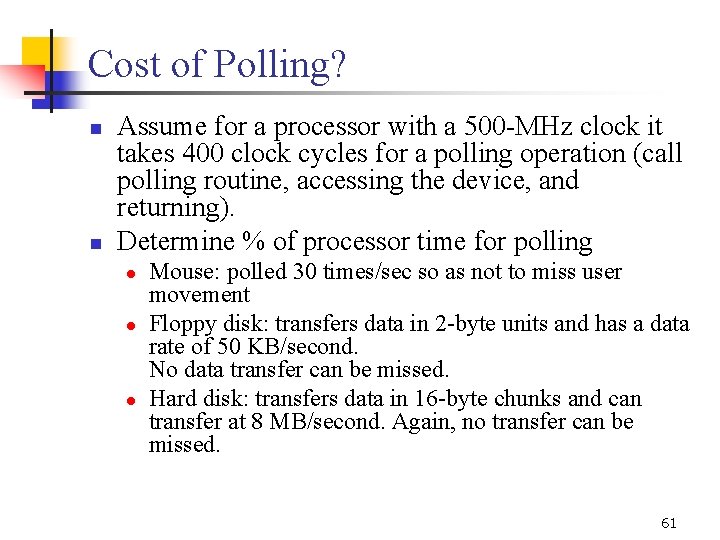
Cost of Polling? n n Assume for a processor with a 500 -MHz clock it takes 400 clock cycles for a polling operation (call polling routine, accessing the device, and returning). Determine % of processor time for polling l l l Mouse: polled 30 times/sec so as not to miss user movement Floppy disk: transfers data in 2 -byte units and has a data rate of 50 KB/second. No data transfer can be missed. Hard disk: transfers data in 16 -byte chunks and can transfer at 8 MB/second. Again, no transfer can be missed. 61

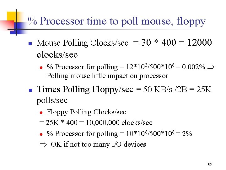
% Processor time to poll mouse, floppy n Mouse Polling Clocks/sec = 30 * 400 = 12000 clocks/sec l n % Processor for polling = 12*103/500*106 = 0. 002% Polling mouse little impact on processor Times Polling Floppy/sec = 50 KB/s /2 B = 25 K polls/sec Floppy Polling Clocks/sec = 25 K * 400 = 10, 000 clocks/sec 6 6 l % Processor for polling = 10*10 /500*10 = 2% OK if not too many I/O devices l 62

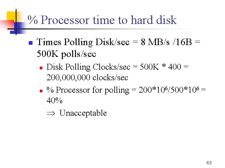
% Processor time to hard disk n Times Polling Disk/sec = 8 MB/s /16 B = 500 K polls/sec l l Disk Polling Clocks/sec = 500 K * 400 = 200, 000 clocks/sec % Processor for polling = 200*106/500*106 = 40% Unacceptable 63

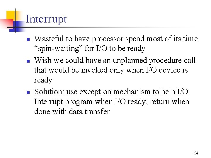
Interrupt n n n Wasteful to have processor spend most of its time “spin-waiting” for I/O to be ready Wish we could have an unplanned procedure call that would be invoked only when I/O device is ready Solution: use exception mechanism to help I/O. Interrupt program when I/O ready, return when done with data transfer 64

Benefit of Interrupt-Driven I/O n n 500 clock cycle overhead for each transfer, including interrupt. Find the % of processor consumed if the hard disk is only active 5% of the time. Interrupt rate = polling rate l l l n Disk Interrupts/sec = 8 MB/s /16 B = 500 K interrupts/sec Disk Polling Clocks/sec = 500 K * 500 = 250, 000 clocks/sec % Processor for during transfer: 250*106/500*106= 50% Disk active 5% * 50% 2. 5% busy 65

Direct Memory Access (DMA) n n n How to transfer data between a Device and Memory? Wastage of CPU cycles if done through CPU. Let the device controller transfer data directly to and from memory DMA The CPU sets up the DMA transfer by supplying the type of operation, memory address and number of bytes to be transferred. The DMA controller contacts the bus directly, provides memory address and transfers the data Once the DMA transfer is complete, the controller interrupts the CPU to inform completion. Cycle Stealing – Bus gives priority to DMA controller thus stealing cycles from the CPU 66

Responsibilities leading to OS n n The I/O system is shared by multiple programs using the processor Low-level control of I/O device is complex because requires managing a set of concurrent events and because requirements for correct device control are often very detailed I/O systems often use interrupts to communicate information about I/O operations Would like I/O services for all user programs under safe control 67