4 bit Lookahead Carry Generator Symbol 16 bit

4 -bit Lookahead Carry Generator Symbol

16 -bit 2 -level Carry Lookahead Adder

Operation of 16 -bit 2 -level Carry Lookahead Adder Signals computed gi , p i i=0. . 15 g[i. . i+3], p[i. . i+3] Formulas g i = xiy i pi = xi y i i=0, 4, 8, 12 g[i. . i+3] = gi+3 + gi+2 pi+3 + gi+1 pi+2 pi+3 + gi pi+1 pi+2 pi+3 p[i. . i+3] = pi pi+1 pi+2 pi+3 Delay 1 gate delay 2 gate delays

16 -bit 2 -level Carry Lookahead Adder

16 -bit 2 -level Carry Lookahead Adder Signals computed ci+1, ci+2, ci+3 Formulas i = 4, 8, 12 i. e. , c 5, c 6, c 7, c 9, c 10, c 11, c 13, c 14, c 15 ci+3 = gi+2 + gi+1 pi+2 + gi pi+1 pi+2 + cipipi+1 pi+2 ci+2 = gi+1 + gi pi+1 + cipipi+1 ci+1 = gi + ci pi Delay 2 gate delays

16 -bit 2 -level Carry Lookahead Adder

64 -bit 3 -level Carry Lookahead Adder c 48 c 32 CLA GEN g[28, 31] c 24 c 28 p[28, 31] CLA GEN g[24, 27] c 19 c 18 c 17 c 23 c 22 c 21 c 27 c 26 c 25 c 31 c 30 c 29 p[24, 27] CLA GEN g[20, 23] c 20 p[20, 23] CLA GEN g[16, 19] c 16 c 0 p[16, 19] CLA GEN g[48, 63] g[32, 47] p[48, 63] p[32, 47] g[16, 31] p[16, 31] CLA GEN g[0, 63] p[0, 63] g[0, 15] p[0, 15]

64 -bit 3 -level Carry Lookahead Adder

Delay of a k-bit Carry-Lookahead Adder Tlookahead-adder = 4 log 4 k

Decimal Adders 8421 weighted coding scheme or BCD Code Decimal Digit BCD 0 0000 1 0001 2 0010 3 0011 4 0100 5 0101 6 0110 7 0111 8 1000 9 1001 Forbidden codes: 1010, 1011, 1100, 1101, 1110, 1111

Decimal Adder •

Comparing Binary and BCD Sums Decimal Sum K -----Same------ 0 -9 10 0 1 0 1 0 0 11 0 1 1 1 0 0 0 1 12 0 1 1 0 0 1 0 13 0 1 1 0 0 1 1 14 0 1 1 1 0 1 0 0 15 0 1 1 1 0 1 16 1 0 0 1 0 17 1 0 0 0 1 1 1 18 1 0 0 1 1 0 0 0 19 1 0 0 1

Decimal Adder •

Rules of BCD adder • When the binary sum is greater than 1001, we obtain a non-valid BCD representation. • The addition of binary 6(0110) to the binary sum converts it to the correct BCD representation and also produces an output carry as required. • To distinguish them from binary 1000 and 1001, which also have a 1 in position Z 8, we specify further that either Z 4 or Z 2 must have a 1. C = K + Z 8 Z 4 + Z 8 Z 2

Implementation of BCD adder • A decimal parallel adder that adds n decimal digits needs n BCD adder stages. • The output carry from one stage must be connected to the input carry of the next higher-order stage. If =1 0110

Binary Multiplier

Two bit Multiplication

Three bit Multiplication • Partial products are: 101 × 1, and 101 × 0 1 • Note that the partial product × 0 1 1 summation for n digit, base 2 1 0 1 numbers requires adding up to n digits (with carries) in 1 0 1 a column. 0 0 0 • Note also n × m digit 0 0 1 multiply 1 1 1 generates up to an m + n digit result (same as decimal).

Multiplier Boolean Equations • • We can also make an n × m “block” multiplier and use that to form partial products. Example: 2 × 2 – The logic equations for each partial-product binary digit are shown below: We need to "add" the columns to get the product bits P 0, P 1, P 2, and P 3. Note that some columns may generate carries. + P 3 b 1 b 0 a 1 a 0 ´ (a 0. b 1) (a 0. b 0) (a 1. b 1) (a 1. b 0) P 2 P 1 P 0

A 2 x 2 binary multiplier • • • The AND gates produce the partial products. For a 2 -bit by 2 -bit multiplier, we can just use two half adders to sum the partial products. In general, though, we’ll need full adders. Here C 3 -C 0 are the product, not carries! HA HA

Multiplication: a special case • In decimal, an easy way to multiply by 10 is to shift all the digits to the left, and tack a 0 to the right end. 128 x 10 = 1280 • We can do the same thing in binary. Shifting left is equivalent to multiplying by 2: 11 x 10 = 110 • Shifting left twice is equivalent to multiplying by 4: 11 x 100 = 1100 • (in decimal, 3 x 2 = 6) (in decimal, 3 x 4 = 12) As an aside, shifting to the right is equivalent to dividing by 2. 110 ÷ 10 = 11 (in decimal, 6 ÷ 2 = 3)

4 x 3 Binary Multiplier

Magnitude Comparator

Two-Bit Comparator
")
Two-Bit Comparator (cont’d)

Equality Comparator XNOR X Y Z Z = X XNOR Y X 0 0 1 1 Y 0 1 Z 1 0 0 1
![4 -bit Equality Detector A[3. . 0] B[3. . 0] Equality Detector A_EQ_B](http://slidetodoc.com/presentation_image_h2/5c86dade956ea9fa8a36c11df8de51ea/image-27.jpg "4 -bit Equality Detector A[3. . 0] B[3. . 0] Equality Detector A_EQ_B")
4 -bit Equality Detector A[3. . 0] B[3. . 0] Equality Detector A_EQ_B

4 -Bit Equality Comparator A 0 B 0 A 1 B 1 A 2 B 2 A 3 B 3 C 0 C 1 C 2 C 3 A_EQ_B
![4 -bit Magnitude Comparator A[3. . 0] B[3. . 0] Magnitude Detector A_LT_B A_EQ_B](http://slidetodoc.com/presentation_image_h2/5c86dade956ea9fa8a36c11df8de51ea/image-29.jpg "4 -bit Magnitude Comparator A[3. . 0] B[3. . 0] Magnitude Detector A_LT_B A_EQ_B")
4 -bit Magnitude Comparator A[3. . 0] B[3. . 0] Magnitude Detector A_LT_B A_EQ_B A_GT_B

Magnitude Comparator How can we find A_GT_B? How many rows would a truth table have? 28 = 256!

Magnitude Comparator Find A_GT_B If A = 1001 and B = 0111 is A > B? Why? Because A 3 > B 3 i. e. A 3. B 3’ = 1 Therefore, one term in the logic equation for A_GT_B is A 3. B 3’

Magnitude Comparator A_GT_B = A 3. B 3’ + …. . Because A 3 = B 3 and A 2 > B 2 i. e. C 3 = 1 and A 2. B 2’ = 1 If A = 1101 and B = 1011 Therefore, the next term in the is A > B? logic equation for A_GT_B is C 3. A 2. B 2’ Why?

Magnitude Comparator A_GT_B = A 3. B 3’ + C 3. A 2. B 2’ + …. . Because A 3 = B 3 and A 2 = B 2 and A 1 > B 1 i. e. C 3 = 1 and C 2 = 1 and If A = 1010 and A 1. B 1’ = 1 B = 1001 Therefore, the next term in the is A > B? logic equation for A_GT_B is C 3. C 2. A 1. B 1’ Why?

Magnitude Comparator A_GT_B = A 3. B 3’ + C 3. A 2. B 2’ + C 3. C 2. A 1. B 1’ + …. . If A = 1011 and B = 1010 is A > B? Why? Because A 3 = B 3 and A 2 = B 2 and A 1 = B 1 and A 0 > B 0 i. e. C 3 = 1 and C 2 = 1 and C 1 = 1 and A 0. B 0’ = 1 Therefore, the last term in the logic equation for A_GT_B is C 3. C 2. C 1. A 0. B 0’

Magnitude Comparator A_GT_B = A 3. B 3’ + C 3. A 2. B 2’ + C 3. C 2. A 1. B 1’ + C 3. C 2. C 1. A 0. B 0’

Magnitude Comparator Find A_LT_B = A 3’. B 3 + C 3. A 2’. B 2 + C 3. C 2. A 1’. B 1 + C 3. C 2. C 1. A 0’. B 0

Code Converters

CODE CONVERTERS • A code converter is a logic circuit that changes data presented in one type of binary code to another type of binary code, such as BCD to binary, BCD to 7 segment, binary to BCD, BCD to XS 3, binary to Gray code, and Gray code to binary. • We know that, two digit decimal values ranging from 00 to 99 can be represented in BCD by two 4 bit code groups.

BCD-to-Binary Conversion One method of BCD-to-Binary code conversion uses adder circuits : 1. The value, or weight, of each bit in the BCD number is represented by a binary number 2. All of the binary representations of the weights of bits that are 1 s in the BCD number are added 3. The result of this addition is the binary equivalent of the BCD number

Contd. . . For example, 4610 is represented as • The MSB has a weight of 10, and the LSB has a weight of 1. • So the most significant 4 bit group represents 40, and the least significant 4 bit group represents 6 as in Table.

Weight Table

The binary equivalent of each BCD bit is a binary number representing the BCD bit weight

The result from the addition of the binary representation for the weights of all the 1 s in the BCD number is the binary number that corresponds to the BCD number.

Example : Convert the BCD equivalent of 26 to binary. Solution
… INPUT ( BINARY) B 3")
FOUR BIT BINARY TO GRAY CODE CONVERTER –DESIGN (1)… INPUT ( BINARY) B 3 B 2 OUTPUTS (GRAY CODE) B 1 B 0 G 3 G 2 G 1 G 0 0 0 1 0 0 0 1 1 0 0 1 0 MSB 0 + 1 + 0 + 1 0 0 0 1 1 0 1 0 1 1 0 0 1 0 1 1 1 0 0 0 1 1 0 0 1 1 1 0 1 0 1 1 1 1 1 0 0 1 0 1 1 1 0 0 1 1 1 0 0 0 Binary code Gray code
… Simplification using K-maps:")
FOUR BIT BINARY TO GRAY CODE CONVERTER –DESIGN (2)… Simplification using K-maps:
 Logic Diagram:")
FOUR BIT BINARY TO GRAY CODE CONVERTER –DESIGN (3) Logic Diagram:
… INPUT ( GRAY CODE) G")
FOUR BIT GRAY CODE TO BINARY CONVERTER –DESIGN (1)… INPUT ( GRAY CODE) G 3 G 2 OUTPUTS (BINARY ) G 1 G 0 B 3 B 2 B 1 B 0 0 0 1 0 0 0 1 1 0 0 0 1 1 1 0 1 0 1 1 0 0 0 1 1 1 0 0 0 1 1 1 0 0 1 1 0 1 0 1 1 0 0 1 1 1 1 0 0 0 1 1 0 1 1 1 1 0 1 0 MSB 1 + 0 + 0 1 1 0 0 0 Gray code Binary code
…")
FOUR BIT GRAY CODE TO BINARY CONVERTER –DESIGN (2)…
…")
FOUR BIT GRAY CODE TO BINARY CONVERTER –DESIGN (3)…
 Logic Diagram:")
FOUR BIT GRAY CODE TO BINARY CONVERTER –DESIGN (4) Logic Diagram:

Exercise 1. Convert the binary number 0101 to Gray code with XOR gates 2. Convert the gray code 1011 to binary with XOR gates Solution:
 Input ( Std BCD code) BCD to XS 3")
Output ( XS 3 Code) Input ( Std BCD code) BCD to XS 3 code converter- Design (1). . . A B C D w x y z 0 0 0 1 1 0 0 0 1 0 0 1 1 0 0 0 1 1 1 0 0 1 1 0 0 1 1 1 1 0 1 0 0 0 1 1 1 0 0 1 0 1 0 X X 1 0 1 1 X X 1 1 0 1 X X 1 1 1 0 X X 1 1 X X
. . .")
BCD to XS 3 code converter- Design (2). . .
. . . • After the manipulation")
BCD to XS 3 code converter- Design (3). . . • After the manipulation of the Boolean expressions for using common gates for two or more outputs, logic expressions can be given by z=D’ y=CD+C’D’ = (C+D)’ x= B’C + B’D + BC’D’ = B’(C+D) + BC’D’ w= A + BC + BD = A + B (C+D)
")
BCD to XS 3 code converter- Design (4)

Decoders, Multiplexers, PLAs Santanu Chattopadhyay Electronics and Electrical Communication Engineering 57

Decoders

DECODER • A decoder is a logic circuit that accepts a set of inputs that represents a binary number and activates only the output that corresponds to the input number. • In other words, a decoder circuit looks at its inputs, determines which binary number is present there, and activates the one output that corresponds to that number ; all other outputs remain inactive

In its general form, a decoder has N input lines to handle N bits and form one to 2 N output lines to indicate the presence of one or more N-bit combinations. The basic binary function • An AND gate can be used as the basic decoding element because it produces a HIGH output only when all inputs are HIGH

Decoding logic for the binary code 1001 with an active-HIGH output.

General decoder diagram # There are 2 N possible input combinations, from A 0 to AN 1. For each of these input combinations only one of the M outputs will be active HIGH (1), all the other outputs are LOW (0).

• If an active-LOW output (74138, one of the output will low and the rest will be high) is required for each decoded number, the entire decoder can be implemented with 1. NAND gates 2. Inverters • If an active-HIGH output (74139, one of the output will high and the rest will be low) is required for each decoded number, the entire decoder can be implemented with • AND gates • Inverters
-Active LOW output (1). . .")
2 -to-4 -Line Decoder (with Enable input)-Active LOW output (1). . .
-Active LOW output (2) • The circuit operates")
2 -to-4 -Line Decoder (with Enable input)-Active LOW output (2) • The circuit operates with complemented outputs and a complement enable input. The decoder is enabled when E is equal to 0. • Only one output can be equal to 0 at any given time, all other outputs are equal to 1. • The output whose value is equal to 0 represents the minterm selected by inputs A and B • The circuit is disabled when E is equal to 1.
")
3 -8 line decoder (active-HIGH)

• This decoder can be referred to in several ways. It can be called a 3 -line-to- 8 -line decoder, because it has three input lines and eight output lines. • It could also be called a binary-octal decoder or converters because it takes a three bit binary input code and activates the one of the eight outputs corresponding to that code. It is also referred to as a 1 -of-8 decoder, because only 1 of the 8 outputs is activated at one time.
")
Logic diagram of 74138 (Example of a 3 Bit Decoder)
 active-LOW")
Truth table of 74138 (Example of a 3 8 Bit Decoder) active-LOW
 • There is an enable function")
74138 (Example of a 3 8 Bit Decoder) • There is an enable function on this device, a LOW level on each input E’ 1, and E’ 2, and a HIGH level on input E 3, is required in order to make the enable gate output HIGH. • The enable is connected to an input of each NAND gate in the decoder, so it must be HIGH for the NAND gate to be enabled. • If the enable gate is not activated then all eight decoder outputs will be HIGH regardless of the states of the three input variables A 0, A 1, and A 2.

Example of a 5 to 32 Bit Decoder
. . .")
4 -line-to-16 line Decoder constructed with two 3 -line-to-8 line decoders (1). . .
 • When")
4 -line-to-16 line Decoder constructed with two 3 -line-to-8 line decoders (2) • When w=0, the top decoder is enabled and the other is disabled. The bottom decoder outputs are all 0’s , and the top eight outputs generate min-terms 0000 to 0111. • When w=1, the enable conditions are reversed. The bottom decoder outputs generate min-terms 1000 to 1111, while the outputs of the top decoder are all 0’s.

Combinational logic implementation

Encoders

Encoder • An encoder is a combinational logic circuit that essentially performs a “reverse” of decoder functions. • An encoder accepts an active level on one of its inputs, representing digit, such as a decimal or octal digits, and converts it to a coded output such as BCD or binary. • Encoders can also be devised to encode various symbols and alphabetic characters. • The process of converting from familiar symbols or numbers to a coded format is called encoding.

• Most decoders accept an input code and produce a HIGH ( or a LOW) at one and only one output line. • In otherworlds , a decoder identifies, recognizes, or detects a particular code. The opposite of this decoding process is called encoding and is performed by a logic circuit called an encoder. • An encoder has a number of input lines, only one of which input is activated at a given time and produces an N-bit output code, depending on which input is activated.

General encoder diagram
![Logic circuit for octal-to binary encoder [8 -line- 3 -line ]](http://slidetodoc.com/presentation_image_h2/5c86dade956ea9fa8a36c11df8de51ea/image-79.jpg "Logic circuit for octal-to binary encoder [8 -line- 3 -line ]")
Logic circuit for octal-to binary encoder [8 -line- 3 -line ]
![Truth table for octal-to binary encoder [8 -line- 3 -line ] A low at](http://slidetodoc.com/presentation_image_h2/5c86dade956ea9fa8a36c11df8de51ea/image-80.jpg "Truth table for octal-to binary encoder [8 -line- 3 -line ] A low at")
Truth table for octal-to binary encoder [8 -line- 3 -line ] A low at any single input will produce the output binary code corresponding to that input. For instance , a low at A 3’ will produce O 2 =0, O 1=1 and O 0 =1, which is binary code for 3. Ao’ is not connected to the logic gates because the encoder outputs always be normally at 000 when none of the inputs is LOW
 (1).")
Design of 4 -input Priority Encoder ( 4 -line-to 2 line priority encoder) (1). . . • A priority encoder is an encoder that includes the priority function • If two or more inputs are equal to 1 at the same time, the input having the highest priority will take precedence. • Truth Table of a 4 -input Priority Encoder: Inputs Outputs D 0 D 1 D 2 D 3 x y V 0 0 X X 0 1 0 0 0 1 X 1 0 0 0 1 1 X X 1 0 1 X X X 1 1
 (2).")
Design of 4 -input Priority Encoder ( 4 -line-to 2 line priority encoder) (2). . . • In addition to two outputs x, and y, the truth table has a third output designated by V, which is a valid bit indicator that is set 1 when one or more inputs are equal to 1. If all inputs are 0, there is no valid input and V is equal to 0. • X’s in the output column indicate don’t care conditions, the X’s in the input columns are useful for representing a truth table in condensed form. • The higher the subscript number, the higher the priority of the input. Input D 3 has the highest priority, so regardless of the values of the other inputs, when this input is 1, the output for xy is 11 (binary 3)
 (3).")
Design of 4 -input Priority Encoder ( 4 -line-to 2 line priority encoder) (3). . . V=D 0+D 1+D 2+D 3 K-Maps for 4 -input Priority Encoder
 (4)")
Design of 4 -input Priority Encoder ( 4 -line-to 2 line priority encoder) (4) Logic Diagram for 4 -input priority encoder

Multiplexers
 A multiplexers (MUX) is a device that allows digital information from")
MULTIPLEXERS (Data Selectors) A multiplexers (MUX) is a device that allows digital information from several sources to be routed onto a single line for transmission over that line to a common destination. The basic multiplexers has several data input lines and a single output line. It also has data- select inputs, which permit digital data on any one of the inputs to be switched to the output line.

MUX-continued. . . A modern stereo system may have a switch that selects music from one of four sources: a cassette tape, CD, a radio tuner , or an auxiliary input such as audio from a VCR or DVD. The switch selects one of the electronic signals from one of these four sources and sends it to the power amplifier and speakers. In simple terms, this is what a multiplexer (MUX) does; it selects one of several input signals and passes it on to the output.

Functional diagram of MUX

Two-input multiplexer

Four-input multiplexer

Logic symbol for a 1 -of-4 data selector/multiplexer.

Logic symbol for a 1 -of-4 data selector/multiplexer. S 1 S 0

Output Waveforms in relation with the Data-Input and Data-Select waveforms - 4 -input MUX The binary state of the data-select inputs during each interval determines which data input is selected. Here the data-select inputs go through a repetitive binary sequence 00, 01, 10, 11, 00, and so on. The resulting output waveform is shown.

8 -input multiplexer

MSI Quad Two input Multiplexer • The 74 LS 157 contain of quad two input multiplexers, I 0 a I 0 b I 0 c I 0 d and I 1 a I 1 b I 1 c I 1 d. • The logic symbol and truth table is shown in Figure. • Notice that each of the four multiplexer shares a common data select line and a common Enable. • Each multiplexer has only one data select input because there are only two groups of inputs to be selected.
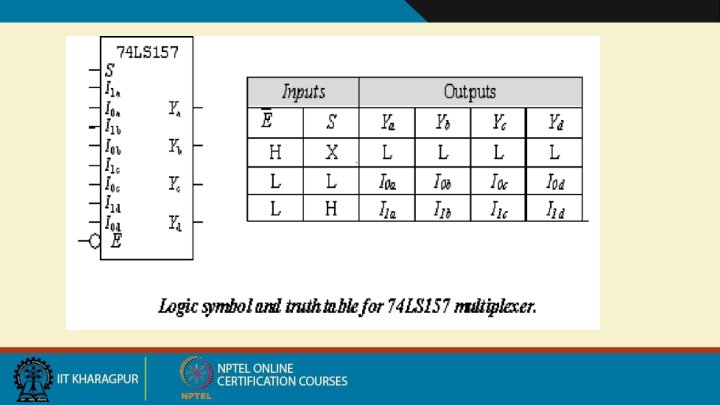

MSI Quad Two input Multiplexer • Input is LOW allows the selected input data to pass through to the output. • Input is HIGH will disable the multiplexers, all of the outputs will be LOW. • When = 0 and S = 1, the Y outputs will follow the set of I 1 inputs, that is Ya = I 1 a , Yb = I 1 b , Yc = I 1 c, and Yd = I 1 d.

LOGIC FUNCTION GENERATION USING MUX Exercise 1: Implement the logic circuit function specified in the table given below by using 74 LS 151 8 -input data selector/multiplexer. Input Output A 2 A 1 A 0 Y 0 0 0 0 1 1 1 0 0 2 0 1 1 1 3 1 0 0 0 4 1 0 1 1 5 1 1 0 1 6 1 1 1 0 7

Solution :

LOGIC FUNCTION GENERATION USING MUX-Method • An efficient method for implementing a Boolean function of n variables with a MUX that has n-1 selection inputs and 2 n-1 data inputs is given below: – List the Boolean function in a truth table – Apply the first n-1 variables in the table to the selection inputs of the MUX. – For each combination of the selection variables, evaluate the output as a function of the last variable. This function can be 0, 1, the variable, or the complement of the variable. Apply these values to the data inputs in the proper order.

LOGIC FUNCTION GENERATION USING MUX-Example 2 Implement the Boolean function F=x’y’z +x’yz’ + xyz using a suitable MUX

LOGIC FUNCTION GENERATION USING MUX-Example 2 • The two variables x and y are applied to the selection lines in that order; x is connected to the S 1 input and y to the S 0 input. • The values for the data input lines are determined from the truth table of the function – For ex. , when xy=00, output F is equal to z because F=0 when z=0 and F=1 when z=1. This requires that variable z is applied to the data input 0

LOGIC FUNCTION GENERATION USING MUX-Example 3 Implement the Boolean function F=A’B’C’D+A’B’CD+A’BC’D’ +AB’CD+ABC’D’+ABC’D+ABCD’+ABCD using a suitable MUX
- Slides: 103