3 DIC Consortium Meeting Marseilles France 18 19
- Slides: 24

3 D-IC Consortium Meeting, Marseilles France, 18 -19 March 2010 Bonding to the detector with DBI 8 OUTLINE: 1) The Frame 2) The Bonding 3) The Targets – more moving than being fixed 4) Design of Detectors 5) Conclusions Grzegorz Deptuch, Ron Lipton, Peter Siddons, Gabriela Carini, Alpana Shenai in close collaboration with Paul Enquist email: deptuch@ieee. org 1

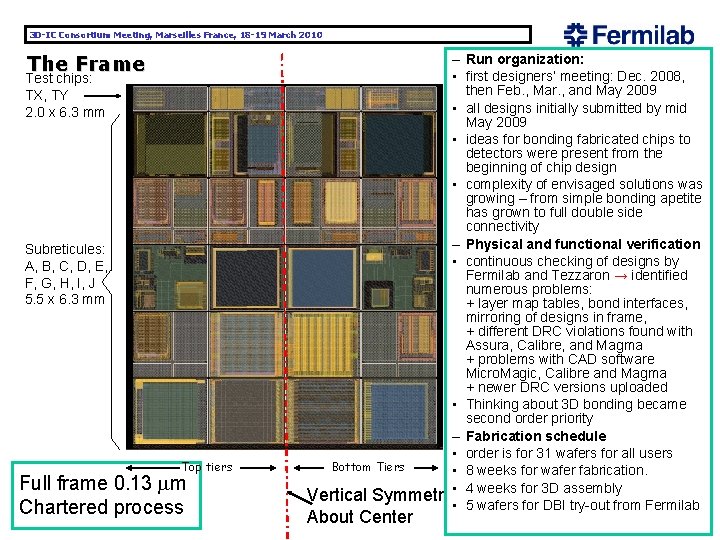
3 D-IC Consortium Meeting, Marseilles France, 18 -19 March 2010 The Frame Test chips: TX, TY 2. 0 x 6. 3 mm Subreticules: A, B, C, D, E, F, G, H, I, J 5. 5 x 6. 3 mm Top tiers Full frame 0. 13 mm Chartered process – Run organization: • first designers’ meeting: Dec. 2008, then Feb. , Mar. , and May 2009 • all designs initially submitted by mid May 2009 • ideas for bonding fabricated chips to detectors were present from the beginning of chip design • complexity of envisaged solutions was growing – from simple bonding apetite has grown to full double side connectivity – Physical and functional verification • continuous checking of designs by Fermilab and Tezzaron → identified numerous problems: + layer map tables, bond interfaces, mirroring of designs in frame, + different DRC violations found with Assura, Calibre, and Magma + problems with CAD software Micro. Magic, Calibre and Magma + newer DRC versions uploaded • Thinking about 3 D bonding became second order priority – Fabrication schedule • order is for 31 wafers for all users Bottom Tiers • 8 weeks for wafer fabrication. Vertical Symmetry • 4 weeks for 3 D assembly • 5 wafers for DBI try-out from Fermilab About Center 2

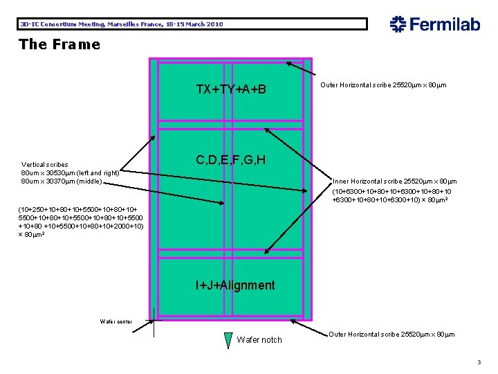
3 D-IC Consortium Meeting, Marseilles France, 18 -19 March 2010 The Frame TX+TY+A+B Vertical scribes 80 um x 30530 mm (left and right) 80 um x 30370 mm (middle) Outer Horizontal scribe 25520 mm x 80 mm C, D, E, F, G, H Inner Horizontal scribe 25520 mm x 80 mm (10+6300+10+80+10+6300+10) × 80 mm 2 (10+250+10+80+10+5500+10+80+10+5500 +10+80 +10+5500+10+80+10+2000+10) × 80 mm 2 I+J+Alignment Wafer center Wafer notch Outer Horizontal scribe 25520 mm x 80 mm 3

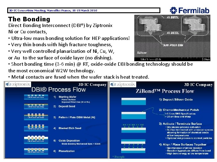
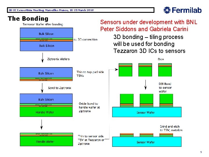
3 D-IC Consortium Meeting, Marseilles France, 18 -19 March 2010 The Bonding Direct Bonding Interconnect (DBI®) by Ziptronix Ni or Cu contacts, • Ultra-low mass bonding solution for HEP applications! • Very thin bonds with high fracture toughness, • Very well controlled planarization of Ni, Cu, W, or Au to the surface of oxide layer (no dishing). • Short bonding time (3 -6 min) @ RT, oxide-oxide DBI bonding technology should be the most economical W 2 W technology. • Metal contacts are fused when the wafer stack is heat treated. 4

3 D-IC Consortium Meeting, Marseilles France, 18 -19 March 2010 The Bonding Sensors under development with BNL Peter Siddons and Gabriela Carini 3 D bonding – tiling process will be used for bonding Tezzaron 3 D ICs to sensors R. Lipton May 8, 2009 5

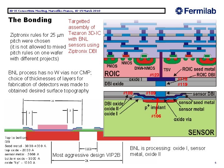
3 D-IC Consortium Meeting, Marseilles France, 18 -19 March 2010 The Bonding Targetted assembly of Ziptronix rules for 25 mm Tezaron 3 D-IC with BNL pitch were chosen (it is not allowed to mixed sensors using pitch rules on one wafer Ziptronix DBI with different projects) BNL process has no W vias nor CMP; choice of thicknesses of layers for fabrication of detectors was made to obtained desired surface topography #123 #108 #119 #106 Most aggressive design VIP 2 B BNL is processing: oxide I, sensor metal, oxide II 6

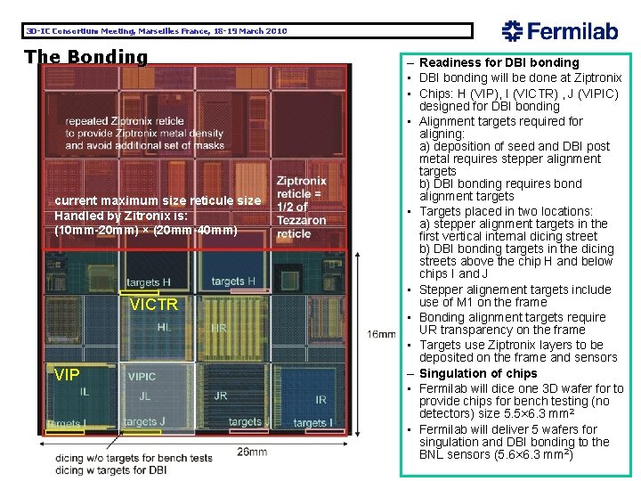
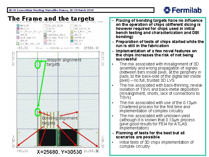
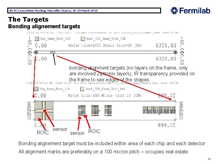
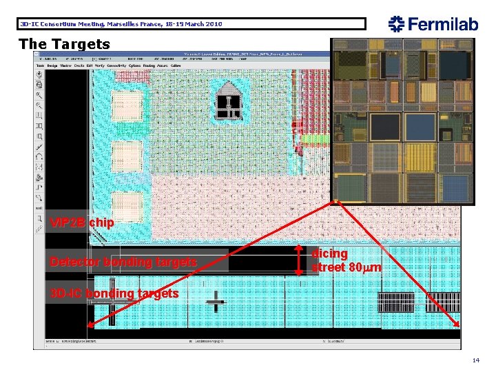
3 D-IC Consortium Meeting, Marseilles France, 18 -19 March 2010 The Bonding current maximum size reticule size Handled by Zitronix is: (10 mm-20 mm) × (20 mm-40 mm) VICTR VIP – Readiness for DBI bonding • DBI bonding will be done at Ziptronix • Chips: H (VIP), I (VICTR) , J (VIPIC) designed for DBI bonding • Alignment targets required for aligning: a) deposition of seed and DBI post metal requires stepper alignment targets b) DBI bonding requires bond alignment targets • Targets placed in two locations: a) stepper alignment targets in the first vertical internal dicing street b) DBI bonding targets in the dicing streets above the chip H and below chips I and J • Stepper alignement targets include use of M 1 on the frame • Bonding alignment targets require UR transparency on the frame • Targets use Ziptronix layers to be deposited on the frame and sensors – Singulation of chips • Fermilab will dice one 3 D wafer for to provide chips for bench testing (no detectors) size 5. 5× 6. 3 mm 2 • Fermilab will deliver 5 wafers for singulation and DBI bonding to the BNL sensors (5. 6× 6. 3 mm 2) 7

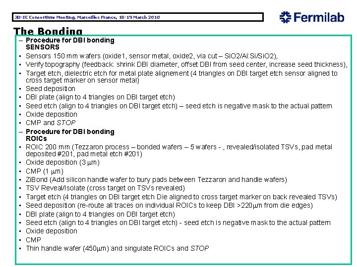
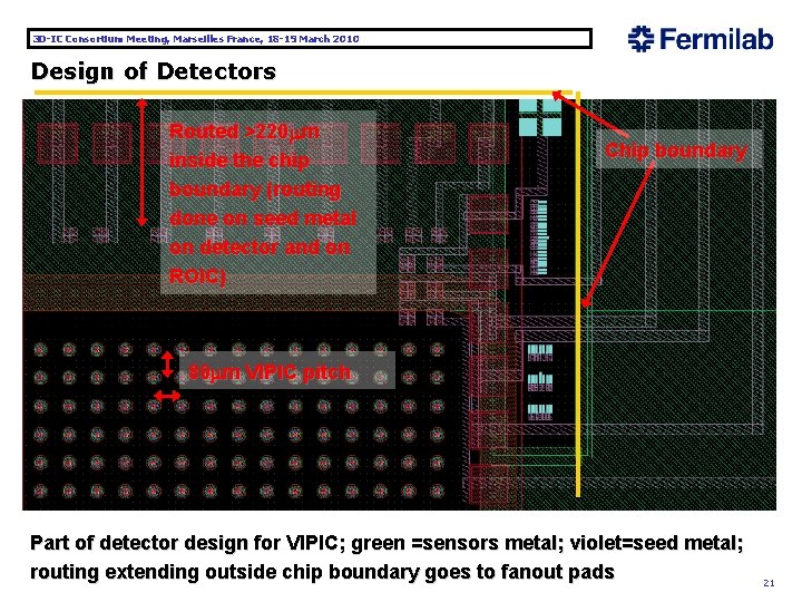
3 D-IC Consortium Meeting, Marseilles France, 18 -19 March 2010 The Bonding – Procedure for DBI bonding SENSORS • Sensors 150 mm wafers (oxide 1, sensor metal, oxide 2, via cut – Si. O 2/Al: Si/Si. O 2), • Verify topography (feedback: shrink DBI diameter, offset DBI from seed center, increase seed thickness), • Target etch, dielectric etch for metal plate alignement (4 triangles on DBI target etch sensor aligned to cross target marker on sensor metal) • Seed deposition • DBI plate (align to 4 triangles on DBI target etch) • Seed etch (align to 4 triangles on DBI target etch) – seed etch is negative mask to the actual pattern • Oxide deposition • CMP and STOP – Procedure for DBI bonding ROICs • ROIC 200 mm (Tezzaron process – bonded wafers – 5 wafers - , revealed/isolated TSVs, pad metal deposited #201, pad metal etch #201) • Oxide deposition (3 mm) • CMP (1 mm) • Zi. Bond (Add silicon handle wafer to bury pads between Tezzaron and handle wafers) • TSV Reveal/Isolate (cross target on TSVs revealed) • Target etch (4 triangles on DBI target etch Die aligned to cross target marker on back revealed TSVs) • Seed deposition (re-route all traces on individual ROICs to keep DBI >220 mm from die edges) • DBI plate (align to 4 triangles on DBI target etch) • Seed etch (align to 4 triangles on DBI target etch) - seed etch is negative mask to the actual pattern • Oxide deposition • CMP • Thin handle wafer (450 mm) and singulate ROICs and STOP 8

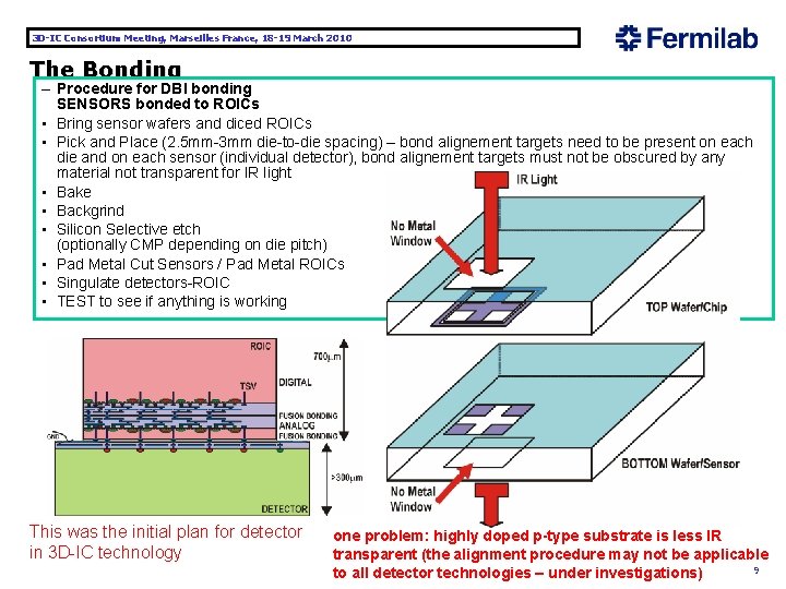
3 D-IC Consortium Meeting, Marseilles France, 18 -19 March 2010 The Bonding – Procedure for DBI bonding SENSORS bonded to ROICs • Bring sensor wafers and diced ROICs • Pick and Place (2. 5 mm-3 mm die-to-die spacing) – bond alignement targets need to be present on each die and on each sensor (individual detector), bond alignement targets must not be obscured by any material not transparent for IR light • Bake • Backgrind • Silicon Selective etch (optionally CMP depending on die pitch) • Pad Metal Cut Sensors / Pad Metal ROICs • Singulate detectors-ROIC • TEST to see if anything is working This was the initial plan for detector in 3 D-IC technology one problem: highly doped p-type substrate is less IR transparent (the alignment procedure may not be applicable 9 to all detector technologies – under investigations)

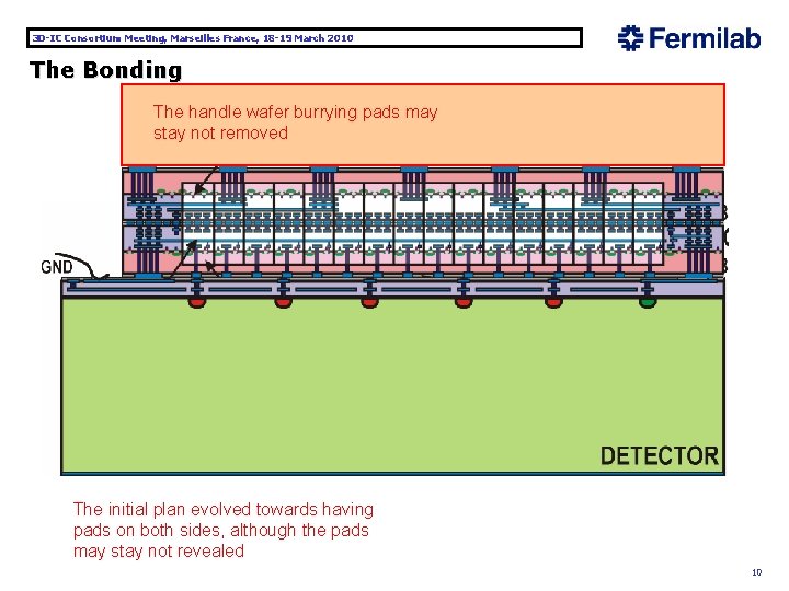
3 D-IC Consortium Meeting, Marseilles France, 18 -19 March 2010 The Bonding The handle wafer burrying pads may stay not removed The initial plan evolved towards having pads on both sides, although the pads may stay not revealed 10

3 D-IC Consortium Meeting, Marseilles France, 18 -19 March 2010 The Frame and the targets – Placing of bonding targets have no influence on the operation of chips (different dicing is however required for chips used in initial bench testing and characterization and DBI bonding) – Preparation of tests of chips started while the run is still in the fabrication – Implementation of a few novel features on the chips increases the risk of not being successful • The risk associated with misalignment of 3 D assembly and wrong propagation of signals (between tiers inside pixel, at the periphery in pads, to the back-side of the digital tier inside pixel) – no full, trusted 3 D LVS • The risk associated with back-thinning, revealisolation of TSVs and back-metal deposition (misalignment, shorts, lack of connections to TSVs) • The risk associated with use of the 0. 13 mm Chartered process for the first time and implementation of complex circuitry • The risk associated with unknown yield (although it is known that 0. 13 mm process gave good results for FEI 4 for ATLAS implementation) – Planning of tests for the best but all scenarios are possible • Initial tests of 3 D chips implementation of complex circuitry stepper alignment targets bonding alignment targets X=25680, Y=30530 X 11

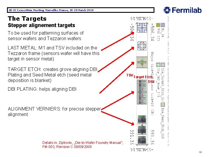
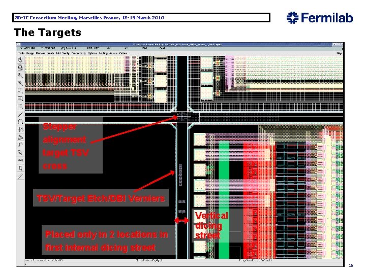
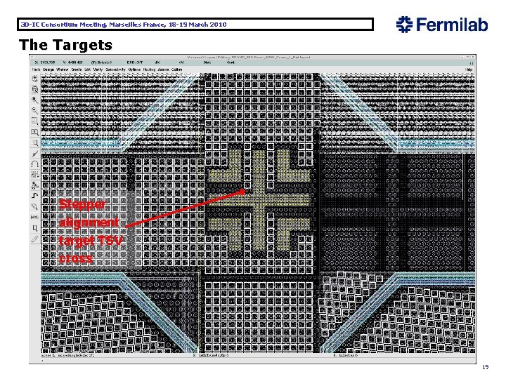
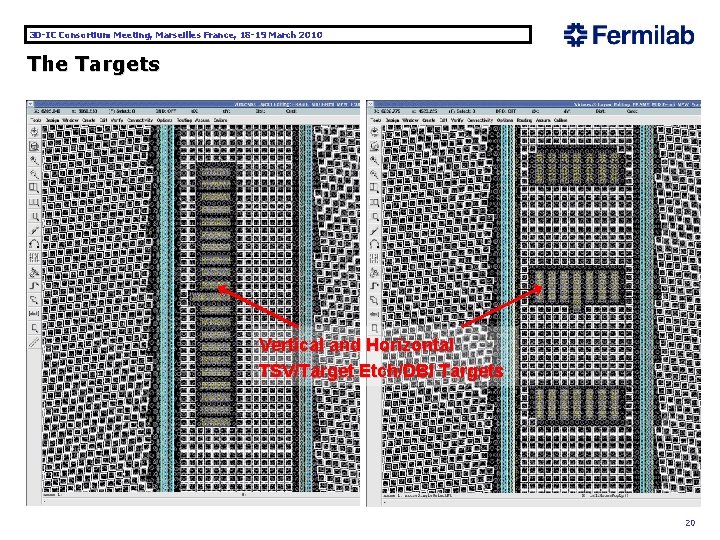
3 D-IC Consortium Meeting, Marseilles France, 18 -19 March 2010 The Targets Stepper alignement targets To be used for patterning surfaces of sensor wafers and Tezzaron wafers LAST METAL: M 1 and TSV included on the Tezzaron frame (sensors wafer will have this target in sensor metal) TARGET ETCH: creates grove aligning DBI Plating and Seed Metal etch (seed metal deposition is blanket) TSV Target Etch DBI PLATING: helps aligning DBI ALIGNMENT VERNIERS: for precise stepper alignment Details in: Ziptronix, „Die-to-Wafer Foundry Manual”, FM-003, Revision C 08/08/2008 12

3 D-IC Consortium Meeting, Marseilles France, 18 -19 March 2010 The Targets Bonding alignement targets bonding alignment targets (no layers on the frame, only are involved Ziptronix layers), IR transparency provided on the frame to see edges of the shapes ROIC sensor ROIC Bonding alignement target must be included within area of each chip and each detector All alignment marks are preferably on a 100 micron pitch – occupies real estate 13

3 D-IC Consortium Meeting, Marseilles France, 18 -19 March 2010 The Targets VIP 2 B chip Detector bonding targets dicing street 80 mm 3 D-IC bonding targets 14

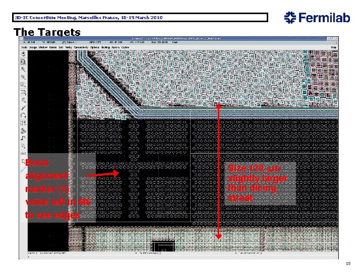
3 D-IC Consortium Meeting, Marseilles France, 18 -19 March 2010 The Targets Bond alignment marker (1) voids left in M 6 to see edges Size 120 mm slightly larger than dicing street 15

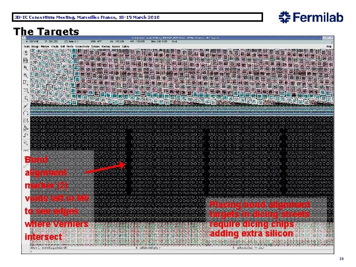
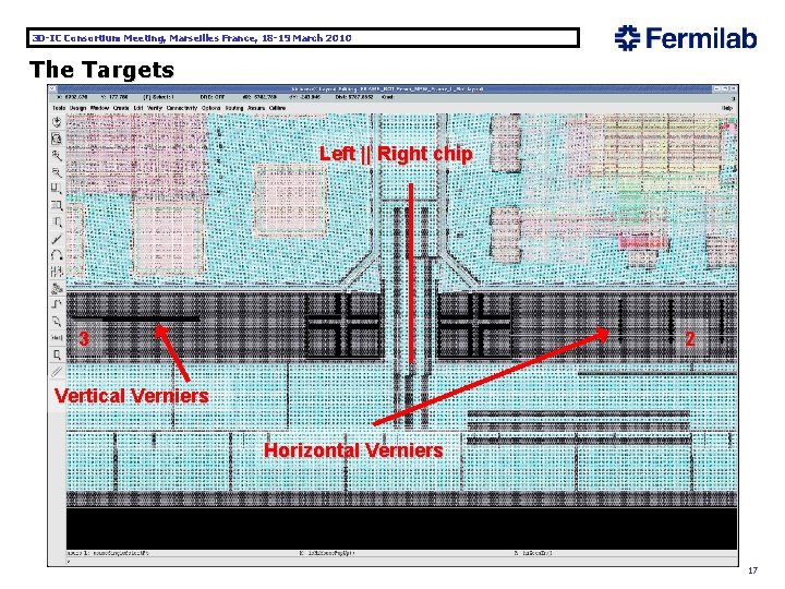
3 D-IC Consortium Meeting, Marseilles France, 18 -19 March 2010 The Targets Bond alignment marker (2) voids left in M 6 to see edges where Verniers intersect Placing bond alignment targets in dicing streets require dicing chips adding extra silicon 16

3 D-IC Consortium Meeting, Marseilles France, 18 -19 March 2010 The Targets Left || Right chip 3 2 Vertical Verniers Horizontal Verniers 17

3 D-IC Consortium Meeting, Marseilles France, 18 -19 March 2010 The Targets Stepper alignment target TSV cross TSV/Target Etch/DBI Verniers Placed only in 2 locations in first internal dicing street Vertical dicing street 18

3 D-IC Consortium Meeting, Marseilles France, 18 -19 March 2010 The Targets Stepper alignment target TSV cross 19

3 D-IC Consortium Meeting, Marseilles France, 18 -19 March 2010 The Targets Vertical and Horizontal TSV/Target Etch/DBI Targets 20

3 D-IC Consortium Meeting, Marseilles France, 18 -19 March 2010 Design of Detectors Routed >220 mm inside the chip boundary (routing done on seed metal on detector and on ROIC) Chip boundary 80 mm VIPIC pitch Part of detector design for VIPIC; green =sensors metal; violet=seed metal; routing extending outside chip boundary goes to fanout pads 21

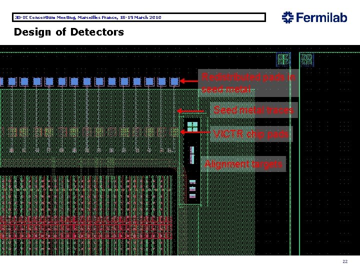
3 D-IC Consortium Meeting, Marseilles France, 18 -19 March 2010 Design of Detectors Redistributed pads in seed metal Seed metal traces VICTR chip pads Alignment targets 22

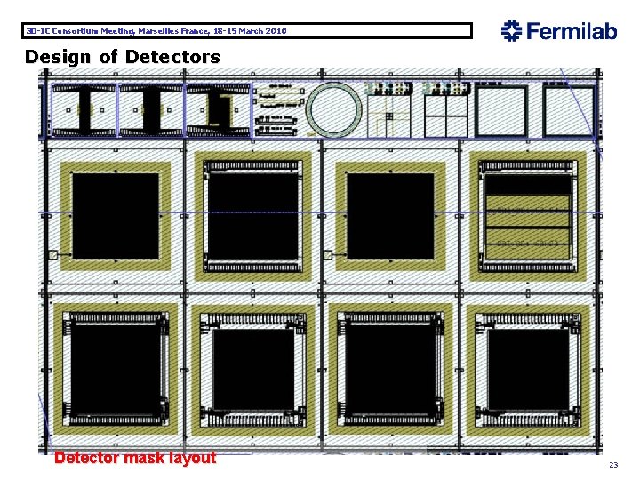
3 D-IC Consortium Meeting, Marseilles France, 18 -19 March 2010 Design of Detectors Detector mask layout 23

3 D-IC Consortium Meeting, Marseilles France, 18 -19 March 2010 Conclusions 8 lack of experience with DBI bonding èdiscoveries of several unpleasant ‘surprises’; some were ‘life threatening’ (initially no targets were included in any chip design, it was not expected how extensive these targets are + condition of not having any DBI within ~200 mm from the chip edge!!!), 8 Luckily all problems got solutions to go around withou modifying chips, 8 Design of dedicated detectors is being accomplished – work with BNL, 8 Most of work is done, however it is believed that still a few steps will need customized approach as not all recommendation (for example grid and placement of individual objects in targets) were respected, 8 Learning all the details on our own, we implemented features potentially allowing DBI on designs from other group (however simultaneous try-out is rather not possible – no mixing of DBI pitches, need for separate lot of wafers, necessity of shooting smaller (than Chartered) reticle size) 8 The BNL sensors experience will be of extreme use for next steps – to involve other detector technologies too 24