3 DIC Consortium Meeting Marseilles France 18 19
- Slides: 31

3 D-IC Consortium Meeting, Marseilles France, 18 -19 March 2010 VIPIC – subreticule J Fermilab ASIC Group, USA Grzegorz Deptuch, Marcel Trimpl, Raymond Yarema AGH UST, POLAND Pawel Grybos, Robert Szczygiel, Ph. D students: Maciej Kachel, Piotr Kmon 8 OUTLINE: 1) Application, 2) Specification, 3) Architecture of VIPIC 4) Mounting options on the detector, 5) Details of circuitry a) Analog, b) Digital, 6) Details of layouts 7) Preparation of tests, 8) Conclusions. email: deptuch@ieee. org 1

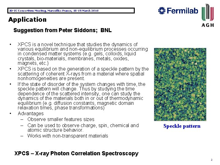
3 D-IC Consortium Meeting, Marseilles France, 18 -19 March 2010 Application Suggestion from Peter Siddons; BNL • • XPCS is a novel technique that studies the dynamics of various equilibrium and non-equilibrium processes occurring in condensed matter systems (e. g. gels, colloids, liquid crystals, bio-materials, membranes, metals, oxides, magnets, etc. ) XPCS is based on the generation of a speckle pattern by the scattering of coherent X-rays from a material where spatial nonhomogeneities are present. If the state of disorder of the system changes with time, the speckle pattern will change. Thus by studying the time dependence of the scattered intensity, one can study the dynamics of the materials both in or out of thermodynamic equilibrium (e. g. diffusion constants, magnetic domain relaxation times, phase transformations) Advantages – Observe smaller features sizes – Can be used to observe charge, spin, chemical and atomic structure behavior. – Works with non-transparent materials Speckle pattern XPCS – X-ray Photon Correlation Spectroscopy 2

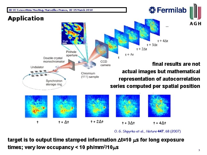
3 D-IC Consortium Meeting, Marseilles France, 18 -19 March 2010 Application final results are not actual images but mathematical representation of autocorrelation series computed per spatial position target is to output time stamped information Dt=10 s for long exposure times; very low occupancy < 10 ph/mm 2/10 s 3

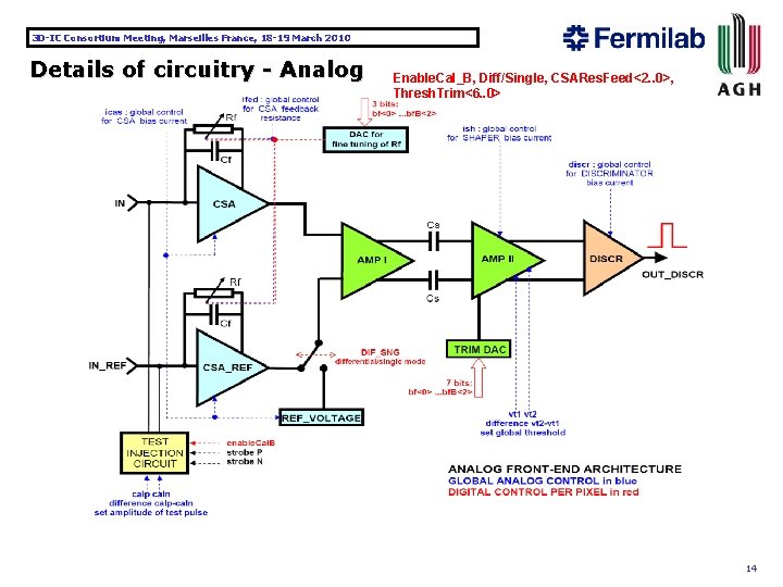
3 D-IC Consortium Meeting, Marseilles France, 18 -19 March 2010 Design specification – Design optimized for 8 ke. V X-ray photons (amplifier range up to 3 × 8 ke. V with Si detector) – 64 × 64 array of 80 mm 2 pixels 5120 × 5120 mm 2 active surface – Die size 5. 5 × 6. 3 mm 2 – 12 -bit DAC for adjustments / pixel (12 × 64 bit long shift register, with 12 -bit latch register/pixel, global analog adjustment of the DAC range) - 7 bit threshold setting / pixel - 3 bit adjustment of feedback resistance in the first stage / pixel - 1 bit selection between single ended and differential architecture / pixel - 1 bit injecting test pulse enable (calibration block with injection capacitance / pixel) – ‘Set’ and ‘Kill’ bits / pixel (two separate shift registers 64 × 64 long, priority of ‘kill’ over ‘set’, ‘kill’ disables reception of hits in digital section – analog stage and discriminator are active) – Shaping time tp=250 ns, power consumption ~25 m. W / analog pixel – Noise <150 e- ENC – Dead timeless operation (operation divided into time slots: hits arriving in time Dtn-1 are read out in Dtn while simultaneously new hits are being acquired in time Dtn) – Sparsified data readout based on priority encoder circuit (binary tree) with automatic binarycoded generation of hit pixel addresses – Hit pixel address readout only (no energy information available) – No trigger acceptance, 4

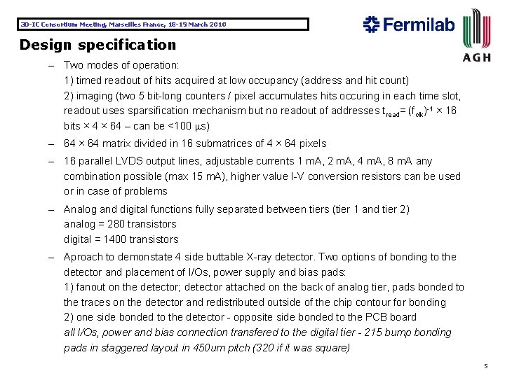
3 D-IC Consortium Meeting, Marseilles France, 18 -19 March 2010 Design specification – Two modes of operation: 1) timed readout of hits acquired at low occupancy (address and hit count) 2) imaging (two 5 bit-long counters / pixel accumulates hits occuring in each time slot, readout uses sparsification mechanism but no readout of addresses tread= (fclk)-1 × 16 bits × 4 × 64 – can be <100 ms) – 64 × 64 matrix divided in 16 submatrices of 4 × 64 pixels – 16 parallel LVDS output lines, adjustable currents 1 m. A, 2 m. A, 4 m. A, 8 m. A any combination possible (max 15 m. A), higher value I-V conversion resistors can be used or in case of problems – Analog and digital functions fully separated between tiers (tier 1 and tier 2) analog = 280 transistors digital = 1400 transistors – Aproach to demonstate 4 side buttable X-ray detector. Two options of bonding to the detector and placement of I/Os, power supply and bias pads: 1) fanout on the detector; detector attached on the back of analog tier, pads bonded to the traces on the detector and redistributed outside of the chip contour for bonding 2) one side bonded to the detector - opposite side bonded to the PCB board all I/Os, power and bias connection transfered to the digital tier - 215 bump bonding pads in staggered layout in 450 um pitch (320 if it was square) 5

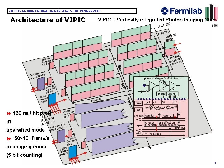
3 D-IC Consortium Meeting, Marseilles France, 18 -19 March 2010 Architecture of VIPIC = Vertically integrated Photon Imaging Chip 8 160 ns / hit pixel in sparsified mode 8 50× 103 frame/s in imaging mode (5 bit counting) 6

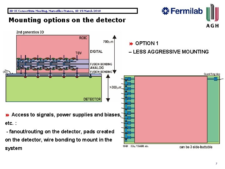
3 D-IC Consortium Meeting, Marseilles France, 18 -19 March 2010 Mounting options on the detector 8 OPTION 1 – LESS AGGRESSIVE MOUNTING 8 Access to signals, power supplies and biases, etc. : - fanout/routing on the detector, pads created on the detector, wire bonding to mount in the system 7

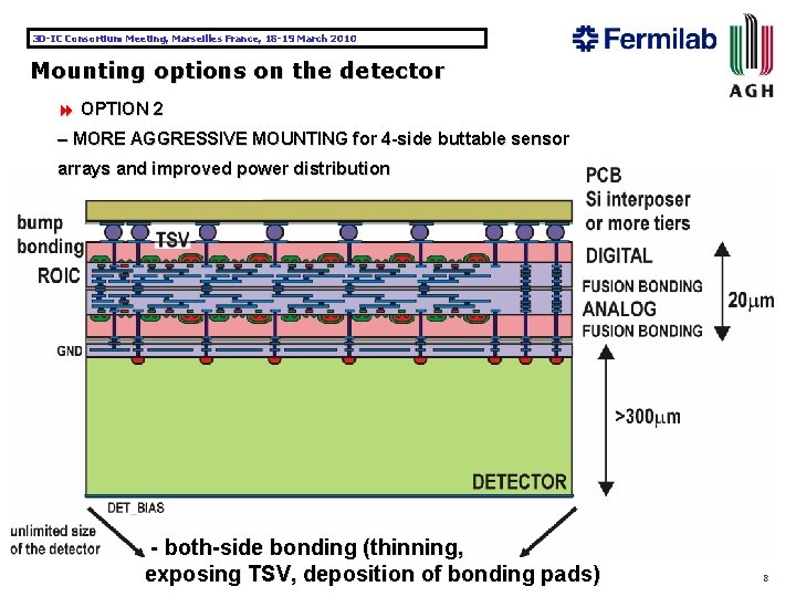
3 D-IC Consortium Meeting, Marseilles France, 18 -19 March 2010 Mounting options on the detector 8 OPTION 2 – MORE AGGRESSIVE MOUNTING for 4 -side buttable sensor arrays and improved power distribution - both-side bonding (thinning, exposing TSV, deposition of bonding pads) 8

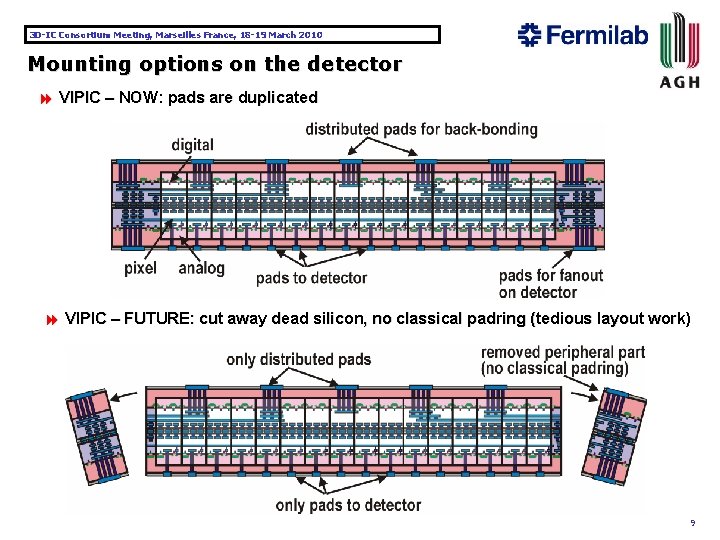
3 D-IC Consortium Meeting, Marseilles France, 18 -19 March 2010 Mounting options on the detector 8 VIPIC – NOW: pads are duplicated 8 VIPIC – FUTURE: cut away dead silicon, no classical padring (tedious layout work) 9

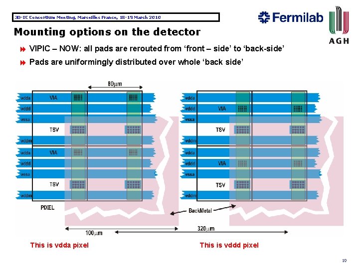
3 D-IC Consortium Meeting, Marseilles France, 18 -19 March 2010 Mounting options on the detector 8 VIPIC – NOW: all pads are rerouted from ‘front – side’ to ‘back-side’ 8 Pads are uniformingly distributed over whole ‘back side’ This is vdda pixel This is vddd pixel 10

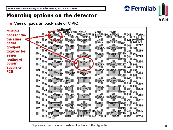
3 D-IC Consortium Meeting, Marseilles France, 18 -19 March 2010 Mounting options on the detector 8 View of pads on back-side of VIPIC Multiple pads for the same nodes grouped together for easier routing of power supply on PCB 11

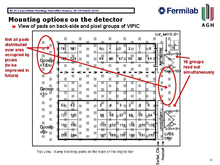
3 D-IC Consortium Meeting, Marseilles France, 18 -19 March 2010 Mounting options on the detector 8 View of pads on back-side and pixel groups of VIPIC Not all pads distributed over area occupied by pixels (to be improved in future) 16 groups read out simultaneously 12

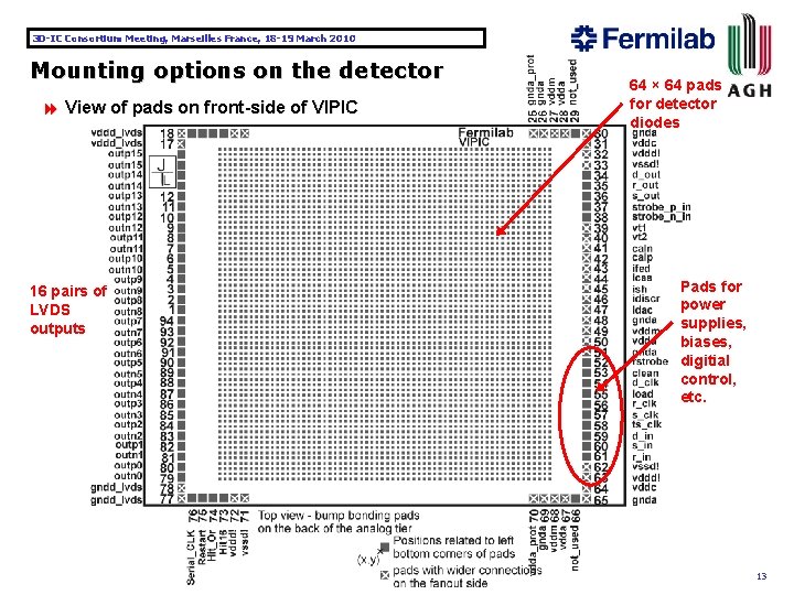
3 D-IC Consortium Meeting, Marseilles France, 18 -19 March 2010 Mounting options on the detector 8 View of pads on front-side of VIPIC 16 pairs of LVDS outputs 64 × 64 pads for detector diodes Pads for power supplies, biases, digitial control, etc. 13

3 D-IC Consortium Meeting, Marseilles France, 18 -19 March 2010 Details of circuitry - Analog Enable. Cal_B, Diff/Single, CSARes. Feed<2. . 0>, Thresh. Trim<6. . 0> 14

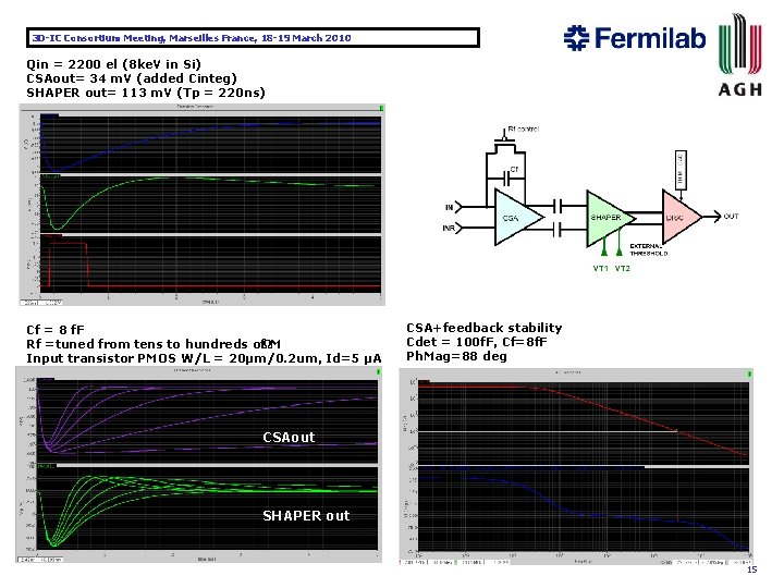
3 D-IC Consortium Meeting, Marseilles France, 18 -19 March 2010 Qin = 2200 el (8 ke. V in Si) CSAout= 34 m. V (added Cinteg) SHAPER out= 113 m. V (Tp = 220 ns) Cf = 8 f. F Rf =tuned from tens to hundreds ofΩM Input transistor PMOS W/L = 20µm/0. 2 um, Id=5 µA CSA+feedback stability Cdet = 100 f. F, Cf=8 f. F Ph. Mag=88 deg CSAout SHAPER out 15

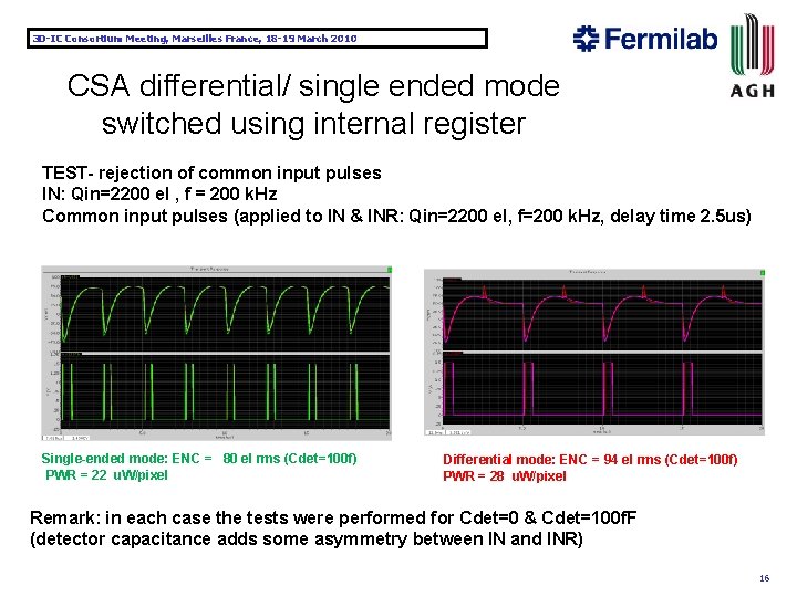
3 D-IC Consortium Meeting, Marseilles France, 18 -19 March 2010 CSA differential/ single ended mode switched using internal register TEST- rejection of common input pulses IN: Qin=2200 el , f = 200 k. Hz Common input pulses (applied to IN & INR: Qin=2200 el, f=200 k. Hz, delay time 2. 5 us) Single-ended mode: ENC = 80 el rms (Cdet=100 f) PWR = 22 u. W/pixel Differential mode: ENC = 94 el rms (Cdet=100 f) PWR = 28 u. W/pixel Remark: in each case the tests were performed for Cdet=0 & Cdet=100 f. F (detector capacitance adds some asymmetry between IN and INR) 16

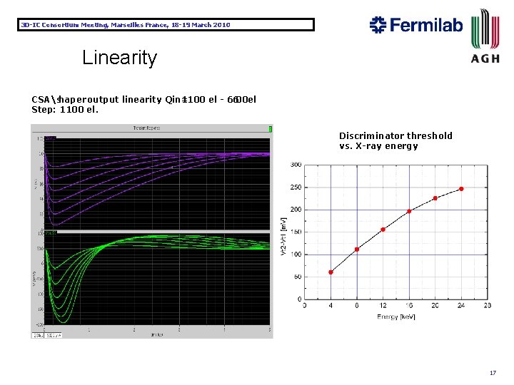
3 D-IC Consortium Meeting, Marseilles France, 18 -19 March 2010 Linearity CSAshaper output linearity Qin= 1100 el - 6600 el Step: 1100 el. Discriminator threshold vs. X-ray energy 17

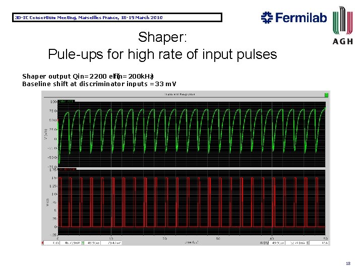
3 D-IC Consortium Meeting, Marseilles France, 18 -19 March 2010 Shaper: Pule-ups for high rate of input pulses Shaper output Qin=2200 elfin=200 k. Hz ( ) Baseline shift at discriminator inputs =33 m. V 18

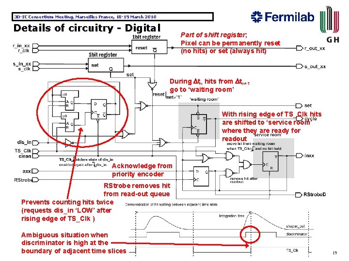
3 D-IC Consortium Meeting, Marseilles France, 18 -19 March 2010 Details of circuitry - Digital Part of shift register; Pixel can be permanently reset (no hits) or set (always hit) During Dtn hits from Dtn+1 go to ‘waiting room’ With rising edge of TS_Clk hits are shifted to ‘service room’ where they are ready for readout Acknowledge from priority encoder RStrobe removes hit from read-out queue Prevents counting hits twice (requests dis_in ‘LOW’ after rising edge of TS_Clk ) Ambiguous situation when discriminator is high at the boundary of adjacent time slices 19

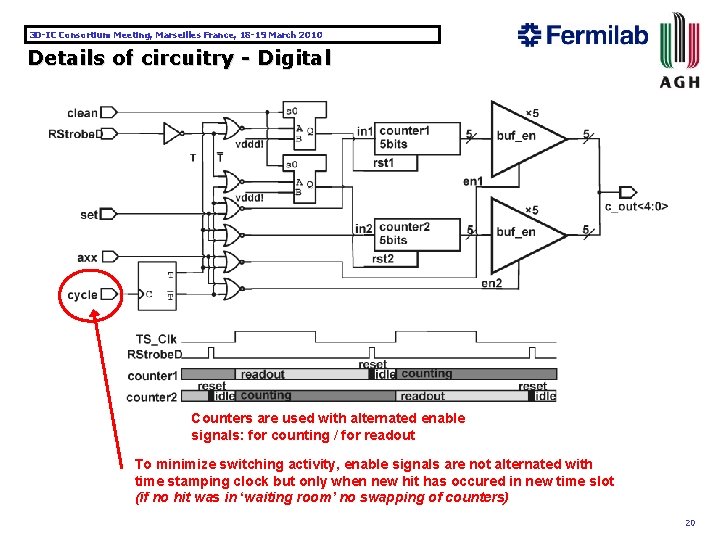
3 D-IC Consortium Meeting, Marseilles France, 18 -19 March 2010 Details of circuitry - Digital Counters are used with alternated enable signals: for counting / for readout To minimize switching activity, enable signals are not alternated with time stamping clock but only when new hit has occured in new time slot (if no hit was in ‘waiting room’ no swapping of counters) 20

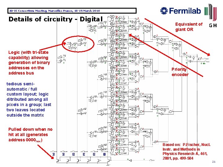
3 D-IC Consortium Meeting, Marseilles France, 18 -19 March 2010 Details of circuitry - Digital Logic (with tri-state capability) allowing generation of binary addresses on the address bus Equivalent of giant OR Priority encoder tedious semiautomatic / full custom layout; logic ditributed among all pixels in a group; last two leaves located outside the matrix Pulled down when no hit at all (generates address 0000 hex) Based on: P. Fischer, Nucl. Instr. and Methods in Physics Research A, 461, 2001, pp. 499 -504 21

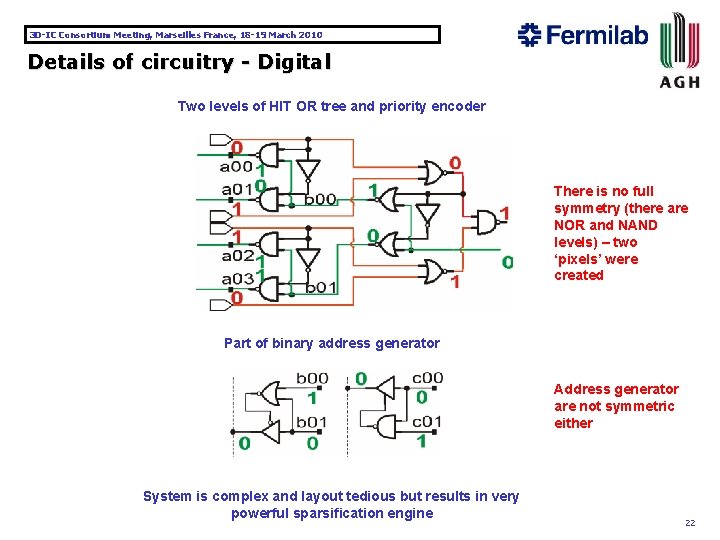
3 D-IC Consortium Meeting, Marseilles France, 18 -19 March 2010 Details of circuitry - Digital Two levels of HIT OR tree and priority encoder There is no full symmetry (there are NOR and NAND levels) – two ‘pixels’ were created Part of binary address generator Address generator are not symmetric either System is complex and layout tedious but results in very powerful sparsification engine 22

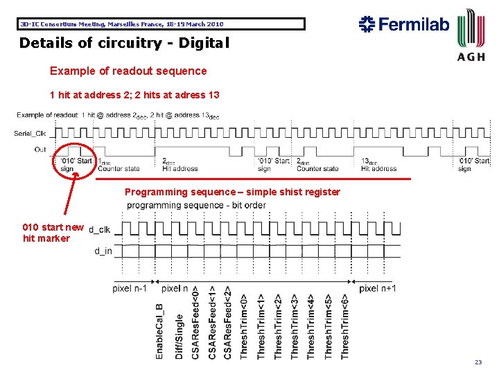
3 D-IC Consortium Meeting, Marseilles France, 18 -19 March 2010 Details of circuitry - Digital Example of readout sequence 1 hit at address 2; 2 hits at adress 13 Programming sequence – simple shist register 010 start new hit marker 23

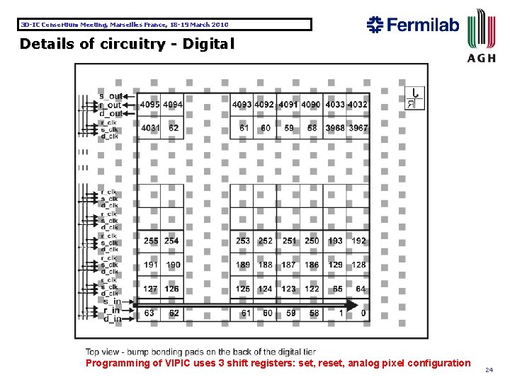
3 D-IC Consortium Meeting, Marseilles France, 18 -19 March 2010 Details of circuitry - Digital Programming of VIPIC uses 3 shift registers: set, reset, analog pixel configuration 24

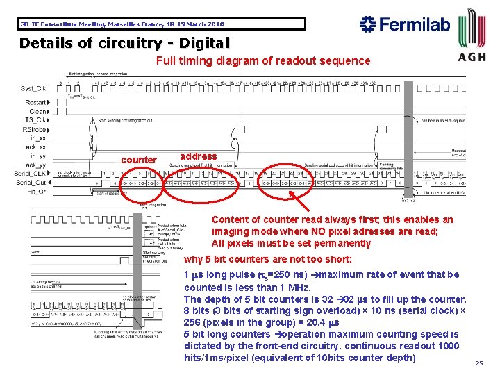
3 D-IC Consortium Meeting, Marseilles France, 18 -19 March 2010 Details of circuitry - Digital Full timing diagram of readout sequence counter address Content of counter read always first; this enables an imaging mode where NO pixel adresses are read; All pixels must be set permanently why 5 bit counters are not too short: 1 s long pulse (ts=250 ns) àmaximum rate of event that be counted is less than 1 MHz, The depth of 5 bit counters is 32 à 32 s to fill up the counter, 8 bits (3 bits of starting sign overload) × 10 ns (serial clock) × 256 (pixels in the group) = 20. 4 s 5 bit long counters àoperation maximum counting speed is dictated by the front-end circuitry. continuous readout 1000 hits/1 ms/pixel (equivalent of 10 bits counter depth) 25

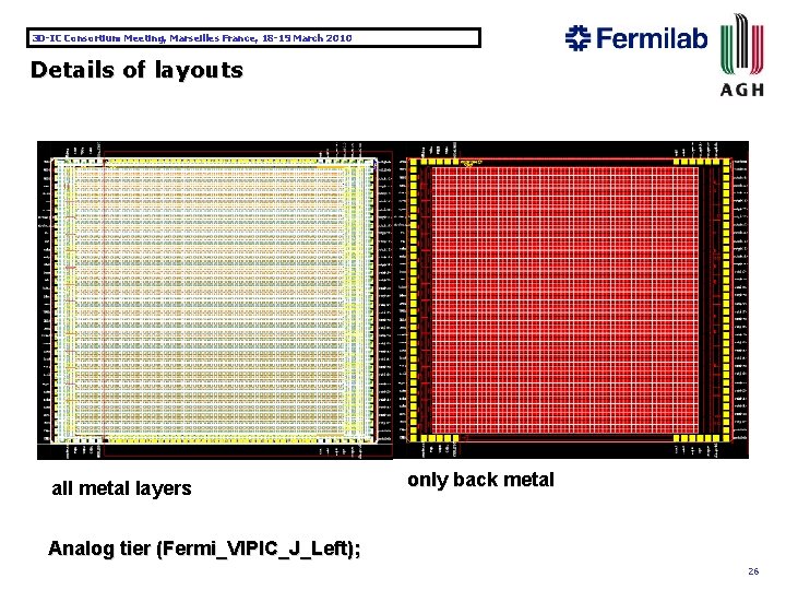
3 D-IC Consortium Meeting, Marseilles France, 18 -19 March 2010 Details of layouts all metal layers only back metal Analog tier (Fermi_VIPIC_J_Left); 26

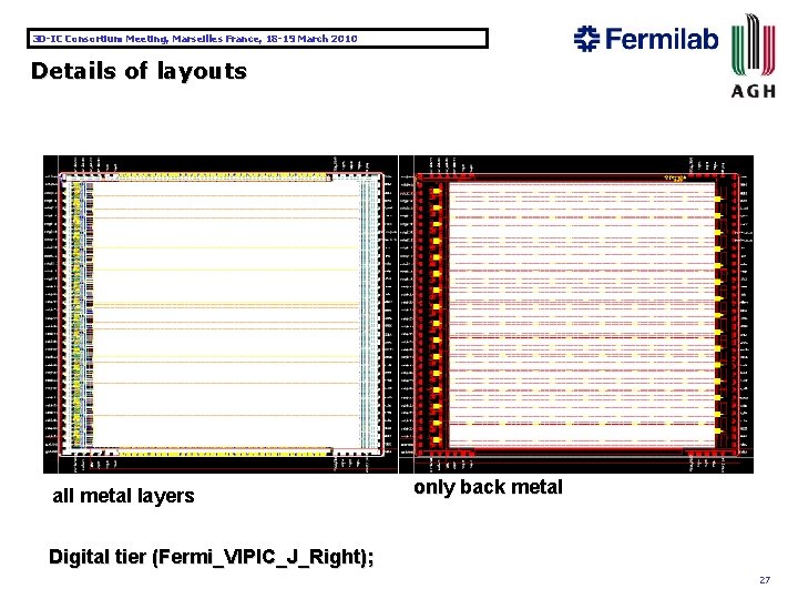
3 D-IC Consortium Meeting, Marseilles France, 18 -19 March 2010 Details of layouts all metal layers only back metal Digital tier (Fermi_VIPIC_J_Right); 27

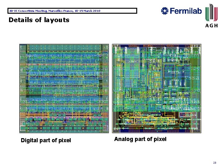
3 D-IC Consortium Meeting, Marseilles France, 18 -19 March 2010 Details of layouts Digital part of pixel Analog part of pixel 28

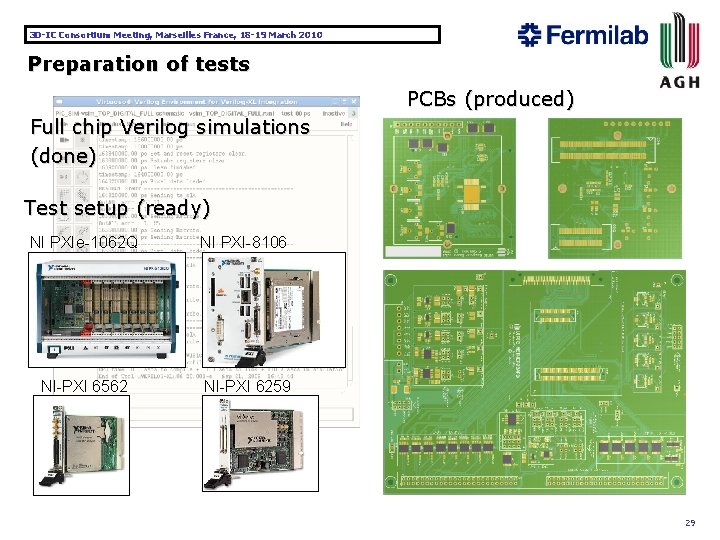
3 D-IC Consortium Meeting, Marseilles France, 18 -19 March 2010 Preparation of tests PCBs (produced) Full chip Verilog simulations (done) Test setup (ready) NI PXIe-1062 Q NI PXI-8106 NI-PXI 6562 NI-PXI 6259 29

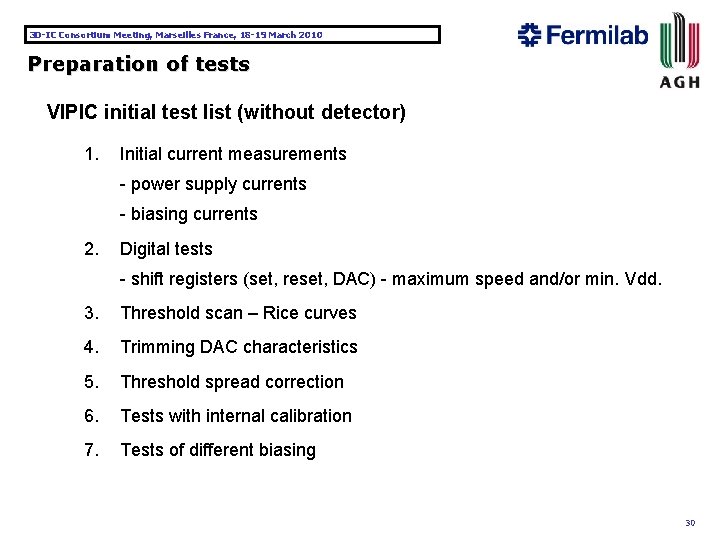
3 D-IC Consortium Meeting, Marseilles France, 18 -19 March 2010 Preparation of tests VIPIC initial test list (without detector) 1. Initial current measurements - power supply currents - biasing currents 2. Digital tests - shift registers (set, reset, DAC) - maximum speed and/or min. Vdd. 3. Threshold scan – Rice curves 4. Trimming DAC characteristics 5. Threshold spread correction 6. Tests with internal calibration 7. Tests of different biasing 30

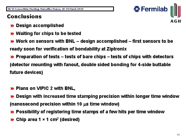
3 D-IC Consortium Meeting, Marseilles France, 18 -19 March 2010 Conclusions 8 Design accomplished 8 Waiting for chips to be tested 8 Work on sensors with BNL – design accomplished – first sensors to be ready soon for verification of bondability at Ziptronix 8 Preparation of tests – tests of bare chips – tests of chips with detectors (detector mounting with fanout, double sided bonding for 4 -side buttable future devices) 8 Plans on VIPIC 2 with BNL, 8 Design with increased time stamping precision within longer time window (nanosecond precision within 10 s time window) 8 Possibility of registering time stamps of a few hits per time window 8 Chip area 1 × 1 cm 2 (desired) 31