Transistor Circuits Ms A A Lande E TC
![2. Transistor in the saturation region [closed switch]: Ø In saturation region, both junctions 2. Transistor in the saturation region [closed switch]: Ø In saturation region, both junctions](https://slidetodoc.com/presentation_image_h/2466c1cd76264af90b3c168212848afe/image-63.jpg)
- Slides: 64

Transistor Circuits Ms. A. A. Lande E & TC Dept

Course outcome • C 302. 2: Select a proper biasing and designing a transistor as an amplifier. Ms. A. A. Lande E & TC Dept

TRANSISTOR CONFIGURATIONS AND BIASING Ms. A. A. Lande E & TC Dept

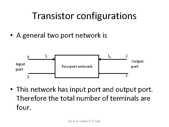
Transistor configurations • A general two port network is 1 Input port Ii Io 2 Output port Two port network 2 1 • This network has input port and output port. Therefore the total number of terminals are four. Ms. A. A. Lande E & TC Dept

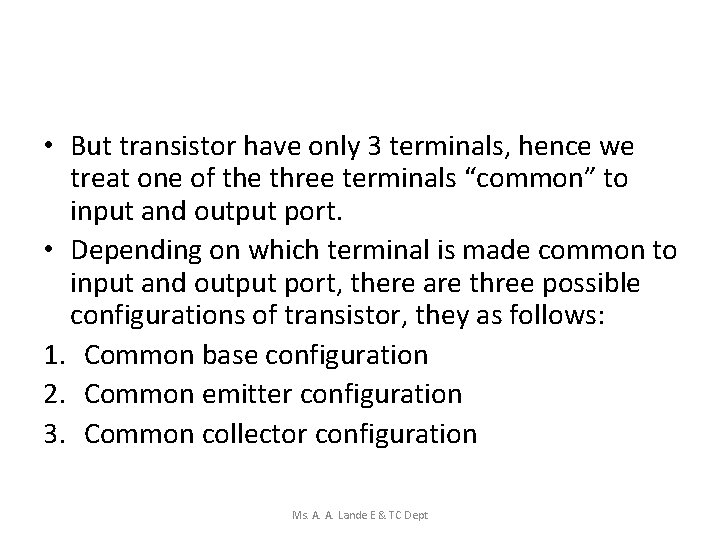
• But transistor have only 3 terminals, hence we treat one of the three terminals “common” to input and output port. • Depending on which terminal is made common to input and output port, there are three possible configurations of transistor, they as follows: 1. Common base configuration 2. Common emitter configuration 3. Common collector configuration Ms. A. A. Lande E & TC Dept

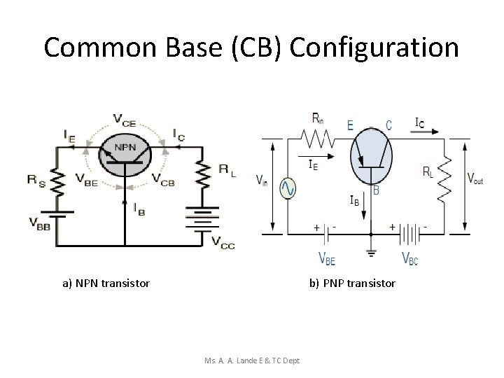
Common Base (CB) Configuration a) NPN transistor b) PNP transistor Ms. A. A. Lande E & TC Dept

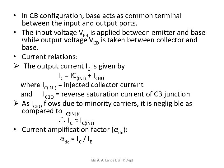
• In CB configuration, base acts as common terminal between the input and output ports. • The input voltage VEB is applied between emitter and base while output voltage VCB is taken between collector and base. • Current relations: Ø The output current IC is given by IC = IC(INJ) + ICBO where IC(INJ) = injected collector current and ICBO = reverse saturation current of CB junction Ø As ICBO flows due to minority carriers, it is negligible as compared to IC(INJ), ∴ IC ≈ IC(INJ) • Current amplification factor (αdc): αdc = IC / IE Ms. A. A. Lande E & TC Dept

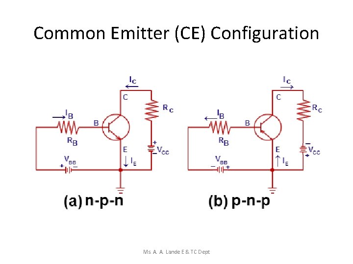
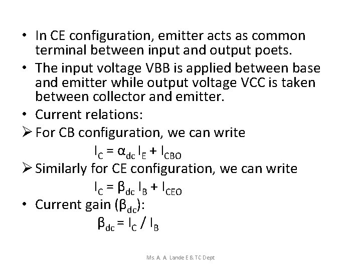
Common Emitter (CE) Configuration Ms. A. A. Lande E & TC Dept

• In CE configuration, emitter acts as common terminal between input and output poets. • The input voltage VBB is applied between base and emitter while output voltage VCC is taken between collector and emitter. • Current relations: Ø For CB configuration, we can write IC = αdc IE + ICBO Ø Similarly for CE configuration, we can write IC = βdc IB + ICEO • Current gain (βdc): βdc = IC / IB Ms. A. A. Lande E & TC Dept

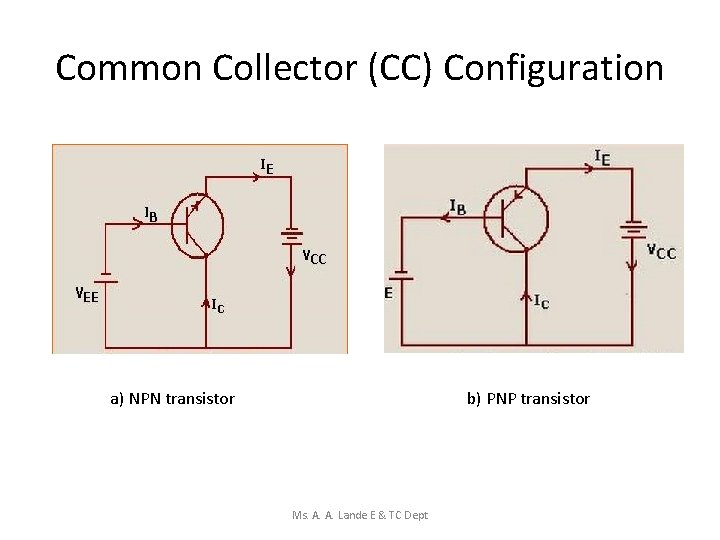
Common Collector (CC) Configuration a) NPN transistor b) PNP transistor Ms. A. A. Lande E & TC Dept

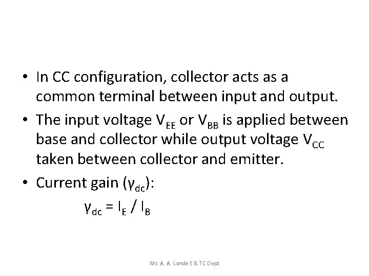
• In CC configuration, collector acts as a common terminal between input and output. • The input voltage VEE or VBB is applied between base and collector while output voltage VCC taken between collector and emitter. • Current gain (γdc): γdc = IE / IB Ms. A. A. Lande E & TC Dept

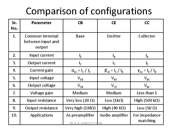
Comparison of configurations Sr. No. Parameter CB CE CC 1. Common terminal between input and output Base Emitter Collector 2. Input current IE IB IB 3. Output current IC IC IE 4. Current gain αdc = IC / IE βdc = IC / IB γdc = IE / IB 5. Input voltage VEB VBE VBC 6. Output voltage VCB VCE VBC 7. Voltage gain Medium Less than 1 8. Input resistance Very low (20 Ω) Low (1 kΩ) High (500 kΩ) 9. Output resistance Very high (1 MΩ) High (40 KΩ) Low (50 Ω) 10. Applications As preamplifier Audio amplifier For impedance matching Ms. A. A. Lande E & TC Dept

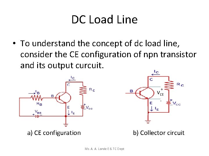
DC Load Line • To understand the concept of dc load line, consider the CE configuration of npn transistor and its output curcuit. + VCE - a) CE configuration b) Collector circuit Ms. A. A. Lande E & TC Dept

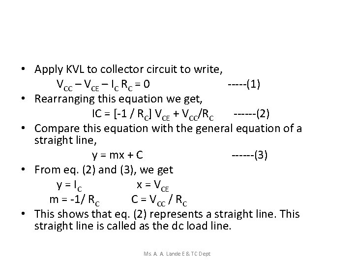
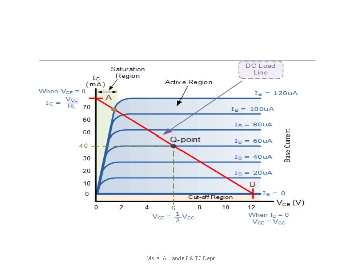
• Apply KVL to collector circuit to write, VCC – VCE – IC RC = 0 -----(1) • Rearranging this equation we get, IC = [-1 / RC] VCE + VCC/RC ------(2) • Compare this equation with the general equation of a straight line, y = mx + C ------(3) • From eq. (2) and (3), we get y = IC x = VCE m = -1/ RC C = VCC / RC • This shows that eq. (2) represents a straight line. This straight line is called as the dc load line. Ms. A. A. Lande E & TC Dept

Ms. A. A. Lande E & TC Dept

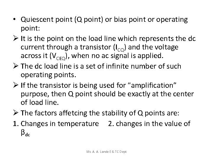
• Quiescent point (Q point) or bias point or operating point: Ø It is the point on the load line which represents the dc current through a transistor (ICQ) and the voltage across it (VCEQ), when no ac signal is applied. Ø The dc load line is a set of infinite number of such operating points. Ø If the transistor is being used for “amplification” purpose, then Q point should be exactly at the center of load line. Ø The factors affetcing the stability of Q points are: 1. Changes in temperature 2. changes in the value of βdc Ms. A. A. Lande E & TC Dept

Biasing circuits • Biasing circuits required to stabilize the position of the Q point or bias point. • Types of biasing circuits: 1. Fixed bias circuit 2. Base bias with emitter feedback 3. Base bias with collector feedback 4. Voltage divider biasing 5. Emitter bias • Out of these, voltage divider biasing circuit is most popularly used. Ms. A. A. Lande E & TC Dept

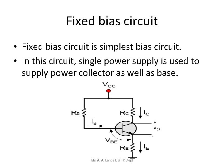
Fixed bias circuit • Fixed bias circuit is simplest bias circuit. • In this circuit, single power supply is used to supply power collector as well as base. + VCE Ms. A. A. Lande E & TC Dept

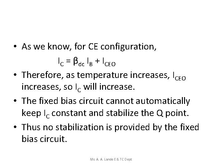
• As we know, for CE configuration, IC = βdc IB + ICEO • Therefore, as temperature increases, ICEO increases, so IC will increase. • The fixed bias circuit cannot automatically keep IC constant and stabilize the Q point. • Thus no stabilization is provided by the fixed bias circuit. Ms. A. A. Lande E & TC Dept

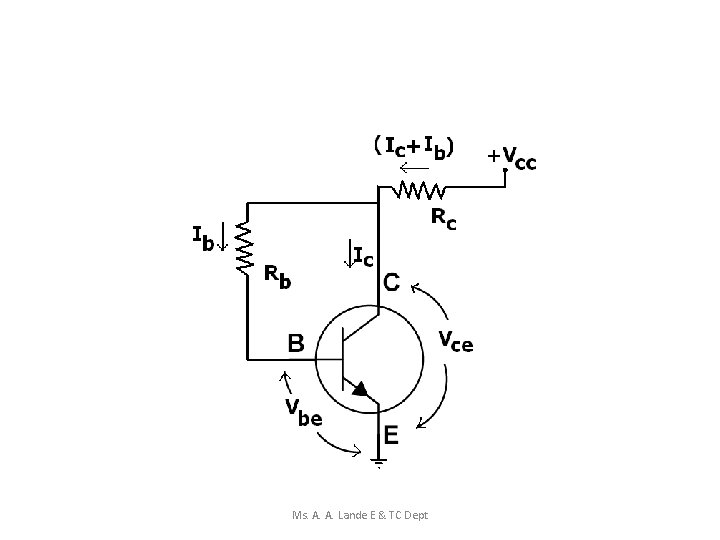
Collector to Base Bias Circuit (Base Bias with Collector Feedback) • Collector to base bias circuit is an improvement over fixed bias circuit. • In this circuit base resistance Rb is connected to collector and not to sypply. • As we know, for CE configuration, IC = βdc IB + ICEO Ms. A. A. Lande E & TC Dept

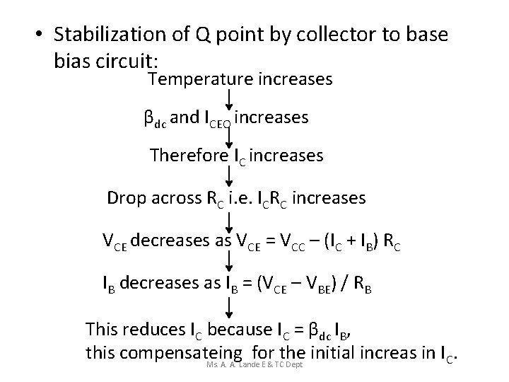
• Stabilization of Q point by collector to base bias circuit: Temperature increases βdc and ICEO increases Therefore IC increases Drop across RC i. e. ICRC increases VCE decreases as VCE = VCC – (IC + IB) RC IB decreases as IB = (VCE – VBE) / RB This reduces IC because IC = βdc IB, this compensateing for the initial increas in IC. Ms. A. A. Lande E & TC Dept

Ms. A. A. Lande E & TC Dept

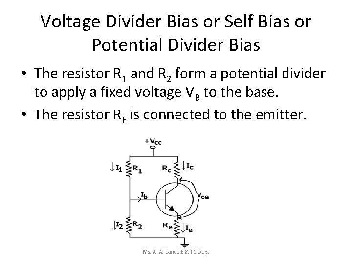
Voltage Divider Bias or Self Bias or Potential Divider Bias • The resistor R 1 and R 2 form a potential divider to apply a fixed voltage VB to the base. • The resistor RE is connected to the emitter. Ms. A. A. Lande E & TC Dept

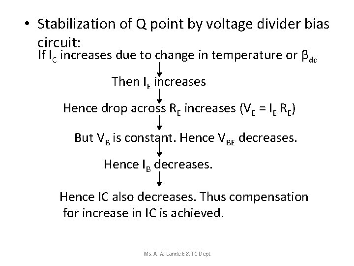
• Stabilization of Q point by voltage divider bias circuit: If IC increases due to change in temperature or βdc Then IE increases Hence drop across RE increases (VE = IE RE) But VB is constant. Hence VBE decreases. Hence IB decreases. Hence IC also decreases. Thus compensation for increase in IC is achieved. Ms. A. A. Lande E & TC Dept

Thermal Runaway • The maximum power that a transistor can dissipate without getting damaged, depends largely on the maximum temperature that collector- base junction can withstand. • The rise in collector- base junction takes place due to two reasons: 1. Due to increase in the ambient temperature 2. Due to the internal heating Ms. A. A. Lande E & TC Dept

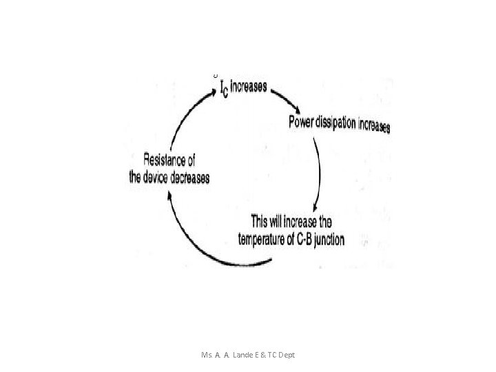
• Out of them the internal heating process is cumulative as explained below: 1. An increase in collector current IC increases the power dissipated in the collector-base junction of the transistor. 2. This will increase the temperature of C-B junction. 3. As the transistor has a negative temperature coefficient of resistivity. , increased junction temperature reduces the resistance. 4. The reduced resistance will increase the collector current further. 5. This becomes a cumulative process which will finally damage the transistor due to excessive internal heating. This process is known as “Thermal Runaway ” Ms. A. A. Lande E & TC Dept

Ms. A. A. Lande E & TC Dept

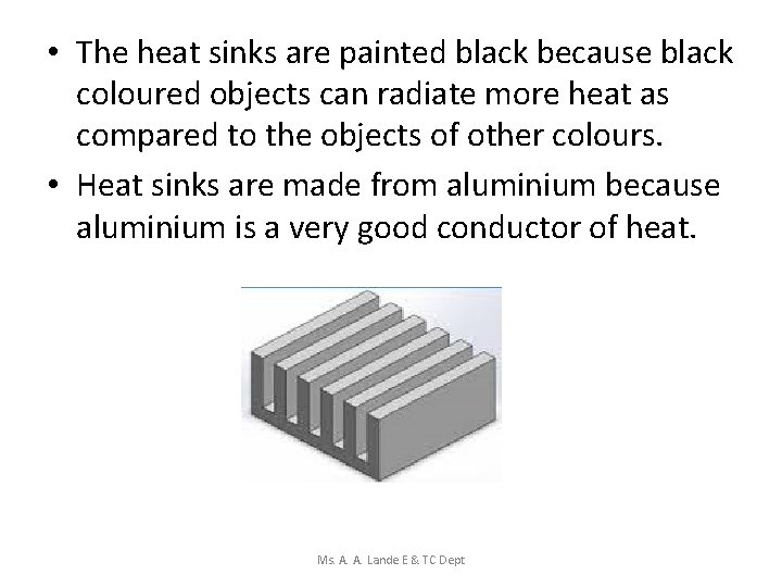
Heat Sink • Heat sinks are large metal pieces of different shapes. • The power transistors are mounted on some form of heat sink but there is no electrical contact between the transistor and heat sink. • When heat sink is used, due to large area of heat sink the heat produced by the transistor is radiated into the air more quickly and easily. • Due to efficient heat radiation by heat sink, the case temperature of the transistor is held to a much lower value. Ms. A. A. Lande E & TC Dept

• The heat sinks are painted black because black coloured objects can radiate more heat as compared to the objects of other colours. • Heat sinks are made from aluminium because aluminium is a very good conductor of heat. Ms. A. A. Lande E & TC Dept

BJT Circuits Ms. A. A. Lande E & TC Dept

Amplification and Amplifier • Amplification: Amplification is a process of adding strength to the input signal or it is a process of “magnifying” the input signal without changing its shape. • Amplifier: Ø The circuit which amplifies a small input signal is called as an “amplifier”. Ø An amplifier is required to amplify weak signals and it is used in radio, TV, telephones, mobile phones, music system etc. Ms. A. A. Lande E & TC Dept

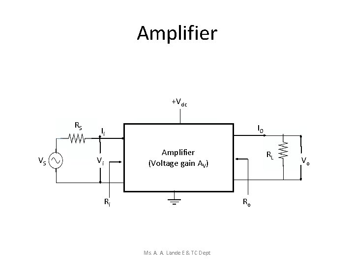
Amplifier +Vdc RS VS IO Ii Amplifier (Voltage gain AV) Vi Ri RL Ro Ms. A. A. Lande E & TC Dept Vo

• In order to magnify the input signal VS all the amplifier need a source of energy which is provided by battery or DC supply. • The dc supply is also essential for biasing the BJT used in amplifier circuits. • The amplifier should contain atleast one active device such as transistor or FET or OPAMP. • If transistor is used then it should be in the active region. Ms. A. A. Lande E & TC Dept

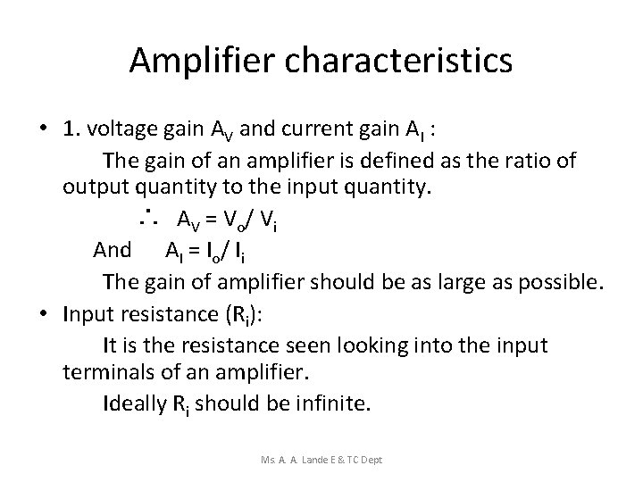
Amplifier characteristics • 1. voltage gain AV and current gain AI : The gain of an amplifier is defined as the ratio of output quantity to the input quantity. ∴ A V = V o/ V i And AI = Io/ Ii The gain of amplifier should be as large as possible. • Input resistance (Ri): It is the resistance seen looking into the input terminals of an amplifier. Ideally Ri should be infinite. Ms. A. A. Lande E & TC Dept

• Output resistance (Ro): It is the resistance seen looking into the output terminals of an amplifier when the input signal Vi = 0 and output circuit is open circuited. Ro should be equal to zero ideally. Ms. A. A. Lande E & TC Dept

Single Stage Amplifier • Depending on which terminal of transistor is made common between input and output, the amplifiers are classified into three types as follows: 1. Common Emitter (CE) amplifier 2. Common Collector (CC) amplifier or emitter follower. 3. Common Base (CB) amplifier Ms. A. A. Lande E & TC Dept

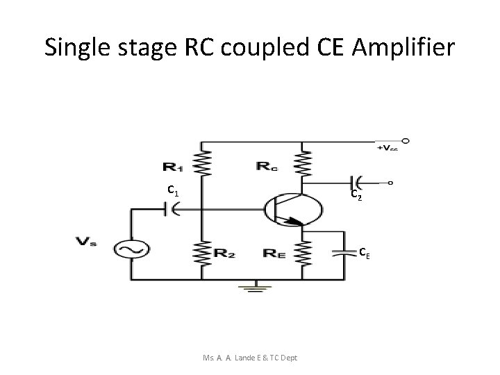
Single stage RC coupled CE Amplifier C 1 C 2 CE Ms. A. A. Lande E & TC Dept

• Fig. shows the a single stage RC coupled CE amplifier. • Circuit Components and their Functions: 1. Resistors: Ø Resistors R 1, R 2 and RE are used to bias the transistor in active region by using voltage divider bias circuit. Ø RC is collector resistor used to control collector current. 2. Input coupling capacitor C 1: Ø The input coupling capacitor C 1 is used to couple the ac input voltage VS to the base of the transistor. Ø As capacitor block dc, C 1 couples only the ac component of the input signal. Ø This capacitor also ensures that the dc biasing conditions of transistor remain unchanged even after applications of the input signal. Ms. A. A. Lande E & TC Dept

3. Bypass capacitor CE: Ø As CE is connected in parallel with RE is called emitter bypass capacitor CE. Ø This capacitor offer a low reactance to the amplified ac signal, therefore RE gets bypassed through CE for only the ac signals. Ø This will increase the voltage gain of the amplifier. 4. Output coupling capacitor C 2: Ø This capacitor couples the amplifier output to the load or to the next stage amplifier. Ø It is used for blocking the dc part and passing only the ac part of the amplified signal to the load. Ms. A. A. Lande E & TC Dept

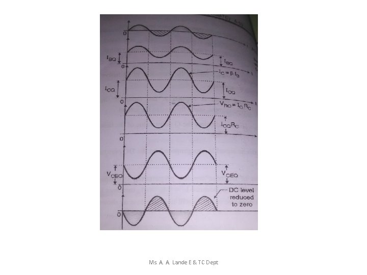
• Operation of the RC coupled amplifier: 1. In the absence of ac input signal current IB = IBQ, IC = ICQ and voltage VCE = VCEQ. The Q point is selected to be in the active region of transistor. 2. As ac input signal VS is applied, the base current varies above and below IBQ. 3. Hence output current IC varies above and below ICQ, because IC = βIB and this variation will be large. 4. As the IC varies, voltage across RC will also varies, because VRC = IC x RC. 5. Hence collector voltage VC varies above and below VCEQ as VC = VCC – ICRC. 6. Through C 2 only the ac part is coupled to the load. Hence Vo is of same shape as VS but of large size. 7. Thus amplification has taken place. Ms. A. A. Lande E & TC Dept

Ms. A. A. Lande E & TC Dept

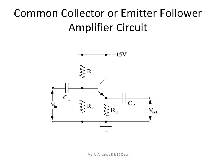
Common Collector or Emitter Follower Amplifier Circuit Ms. A. A. Lande E & TC Dept

• In CC amplifier, input signal is applied at base and output is obtained at emitter. • Why is CC amplifier called as emitter follower? Ø The voltage gain of CC amplifier is almost equal to 1. Therefore input and output voltages are equal and in phase with each other. Ø Hence it is said that output (emitter) follows the input voltage. Hence the name is emitter follower. Ms. A. A. Lande E & TC Dept

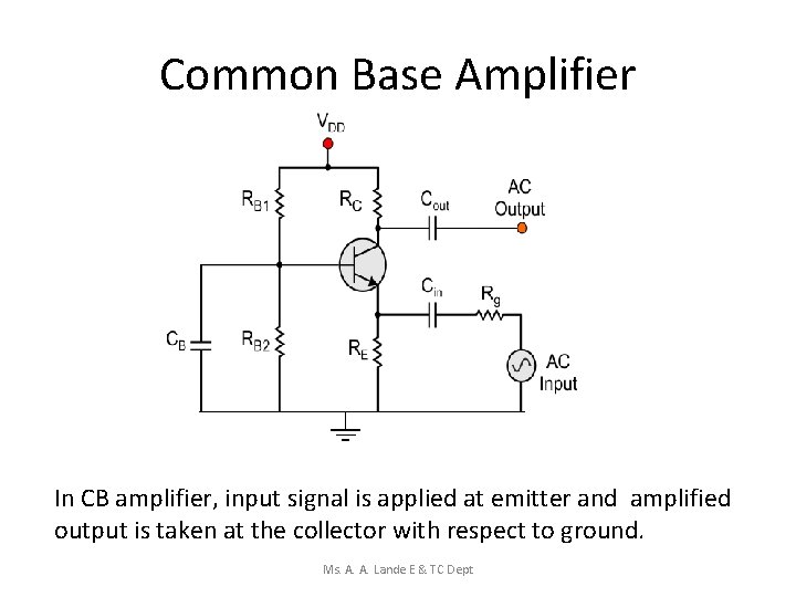
Common Base Amplifier In CB amplifier, input signal is applied at emitter and amplified output is taken at the collector with respect to ground. Ms. A. A. Lande E & TC Dept

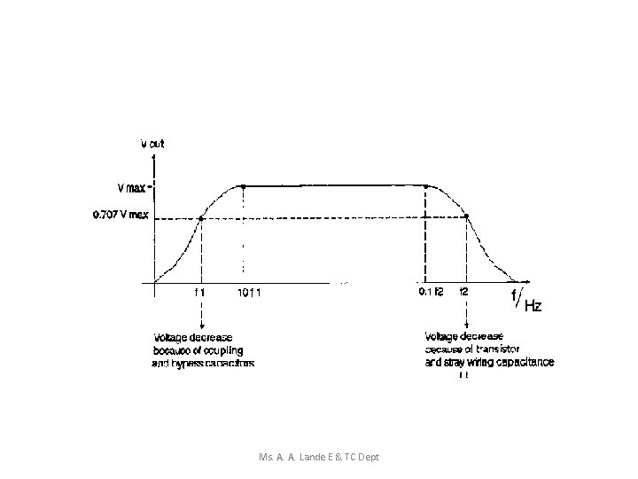
Frequency Response and Bandwidth • The frequency response is graph of amplifier output voltage (or gain) versus the frequency of input signal. • Ideally frequency response should be flat over the entire frequency range. • Practically the frequency response of an amplifier is not flat over the entire operating frequency region. Ms. A. A. Lande E & TC Dept

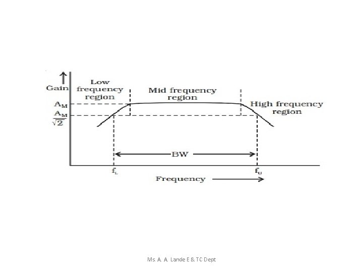
• The practical frequency response can be divided into three regions as follows: 1. Low frequency region. 2. Mid frequency region. 3. High frequency region. 1. Low frequency region: In low frequency region, the gain or output voltage decreases due to the increased reactance of the coupling and bypass capacitor. 2. Mid frequency region: In this region, gain and output voltage remain constant. 3. High frequency region: In this region, the output voltage and gain will decrease due to the transistor internal capacitances and stray capacitance. Ms. A. A. Lande E & TC Dept

• Bandwidth: Ø Bandwidth is the band of frequencies in which the magnitude of output voltage or gain is either equal or relatively close to their mid frequency band value. Ø The frequencies f. L and f. H are called cutoff frequencies or half power frequencies. Ø Bandwidth of the amplifier is defined as the difference between the half power frequencies. • Lower cutoff frequency (f 1 or f. L): It is the frequency of the input signal at which the amplifier gain or output voltage reduce to 70. 7% of their mid frequency range value. f 1 is always less than f 2. • Upper cutoff frequency (f 2 or f. H): It is the frequency of the input signal at which the amplifier output voltage reduce to 70. 7% of their mid frequency range value. f 2 is always higher than f 1. Ms. A. A. Lande E & TC Dept

Ms. A. A. Lande E & TC Dept

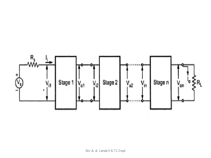
Multistage Transistor Amplifier • The multistage amplifier is obtained by cascading a number of amplifiers i. e. connecting a number of amplifier stages to each other with the output of the previous stage to the input of next stage. • The most important parameters of an amplifier are its input impedance, voltage gain, bandwidth and output resistance which are dependent on the particular applications. • In general, a single stage amplifier is not capable to fulfill all these requirements. Hence we have to use a multistage amplifier. Ms. A. A. Lande E & TC Dept

Ms. A. A. Lande E & TC Dept

Overall Gain of the Multistage Amplifier • Overall voltage gain: Let AV 1, AV 2, AV 3…. AVn be the voltage gain of n number stages of multistage amplifier. Then total voltage gain AV of multistage amplifier is given by AV = AV 1 x AV 2 x AV 3 x ……. x Avn • Overall current gain: Similarly, overall current gain AI of multistage amplifier having n number of stages is given by AI = AI 1 x AI 2 x AI 3 x ……. . x AIn • Overall input resistance (Ri): the overall input resistance of a cascaded amplifier is equal to the input resistance of the first stage. Ms. A. A. Lande E & TC Dept

• Overall output resistance (Ro): The overall output resistance of a cascaded amplifier is equal to the output resistance of the last stage. • Gain in decibels: The gain expressed as a ratio of output voltage and input voltage is called as the linear gain. On the logarithmic scale the gain is expressed in decibels as follows: 1. Power gain in d. B = 10 log 10 [Po/ Pi] 2. Voltage gain in d. B = 20 log 10 [Vo/ Vi] Ms. A. A. Lande E & TC Dept

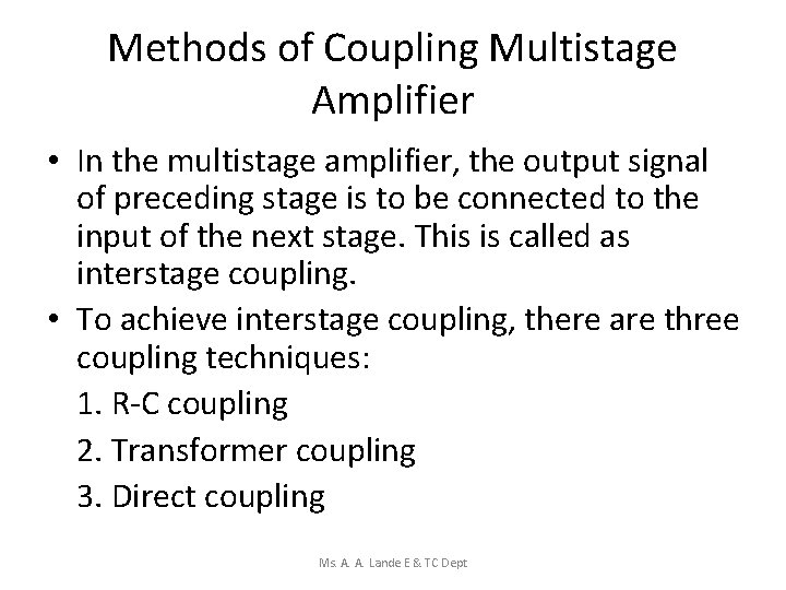
Methods of Coupling Multistage Amplifier • In the multistage amplifier, the output signal of preceding stage is to be connected to the input of the next stage. This is called as interstage coupling. • To achieve interstage coupling, there are three coupling techniques: 1. R-C coupling 2. Transformer coupling 3. Direct coupling Ms. A. A. Lande E & TC Dept

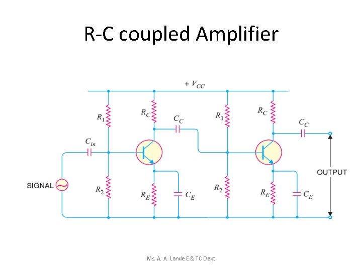
R-C coupled Amplifier Ms. A. A. Lande E & TC Dept

Ms. A. A. Lande E & TC Dept

• Applications: 1. In public address (P. A. ) amplifier system 2. Tape recorders 3. TV, VCR and CD players 4. Stereo amplifier • RC coupled amplifier are basically voltage amplifier. Ms. A. A. Lande E & TC Dept

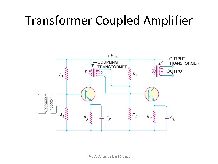
Transformer Coupled Amplifier Ms. A. A. Lande E & TC Dept

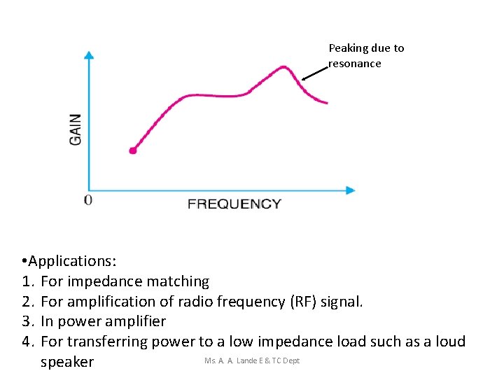
Peaking due to resonance • Applications: 1. For impedance matching 2. For amplification of radio frequency (RF) signal. 3. In power amplifier 4. For transferring power to a low impedance load such as a loud Ms. A. A. Lande E & TC Dept speaker

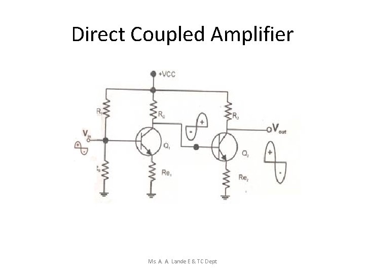
Direct Coupled Amplifier Ms. A. A. Lande E & TC Dept

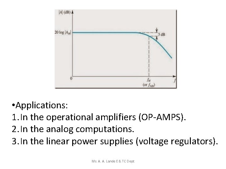
• Applications: 1. In the operational amplifiers (OP-AMPS). 2. In the analog computations. 3. In the linear power supplies (voltage regulators). Ms. A. A. Lande E & TC Dept

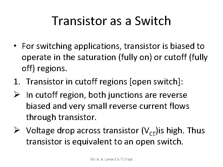
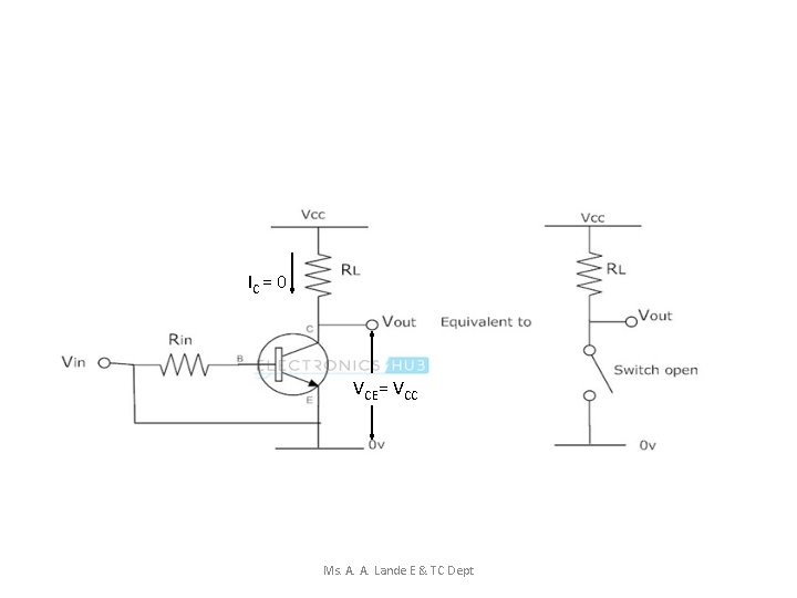
Transistor as a Switch • For switching applications, transistor is biased to operate in the saturation (fully on) or cutoff (fully off) regions. 1. Transistor in cutoff regions [open switch]: Ø In cutoff region, both junctions are reverse biased and very small reverse current flows through transistor. Ø Voltage drop across transistor (VCE)is high. Thus transistor is equivalent to an open switch. Ms. A. A. Lande E & TC Dept

IC = 0 VCE= VCC Ms. A. A. Lande E & TC Dept
![2 Transistor in the saturation region closed switch Ø In saturation region both junctions 2. Transistor in the saturation region [closed switch]: Ø In saturation region, both junctions](https://slidetodoc.com/presentation_image_h/2466c1cd76264af90b3c168212848afe/image-63.jpg)
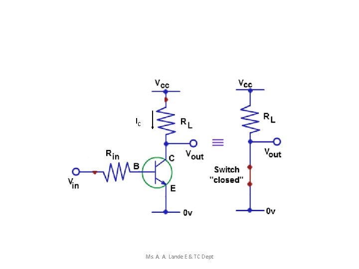
2. Transistor in the saturation region [closed switch]: Ø In saturation region, both junctions are forward biased. The voltage drop across the transistor is very small and collector current is very large. Ø Thus in this region, transistor equivalent to a closed switch. Ms. A. A. Lande E & TC Dept

IC Ms. A. A. Lande E & TC Dept