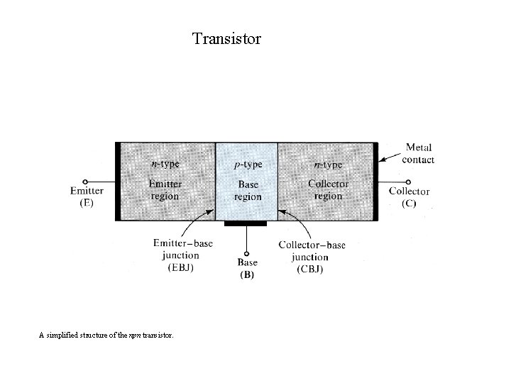
Transistor A simplified structure of the npn transistor
- Slides: 24

Transistor A simplified structure of the npn transistor.

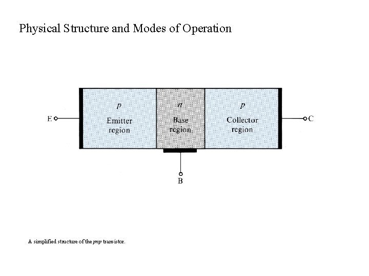
Physical Structure and Modes of Operation A simplified structure of the pnp transistor.

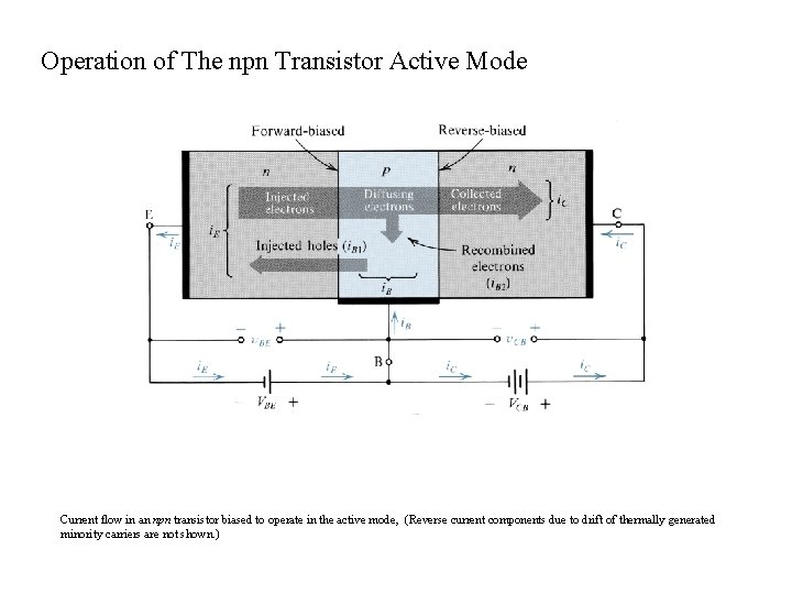
Operation of The npn Transistor Active Mode Current flow in an npn transistor biased to operate in the active mode, (Reverse current components due to drift of thermally generated minority carriers are not shown. )

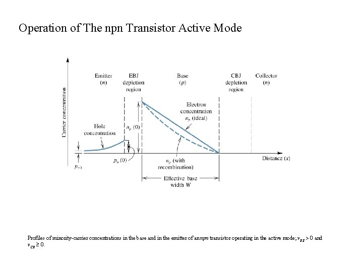
Operation of The npn Transistor Active Mode Profiles of minority-carrier concentrations in the base and in the emitter of an npn transistor operating in the active mode; v. BE 0 and v. CB 0.

Operation of The npn Transistor Active Mode Current Flow The Collector Current The Base Current The Emitter Current

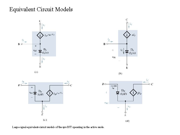
Equivalent Circuit Models Large-signal equivalent-circuit models of the npn BJT operating in the active mode.

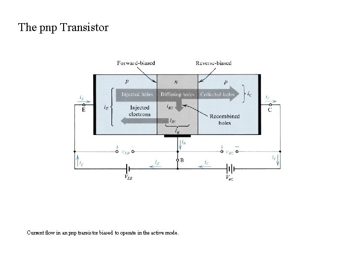
The pnp Transistor Current flow in an pnp transistor biased to operate in the active mode.

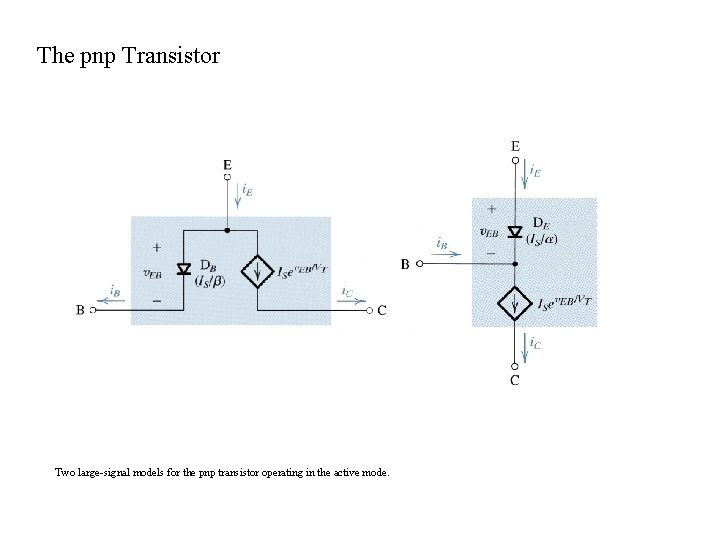
The pnp Transistor Two large-signal models for the pnp transistor operating in the active mode.

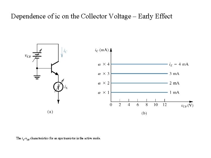
Dependence of ic on the Collector Voltage – Early Effect The i. C-v. CB characteristics for an npn transistor in the active mode.

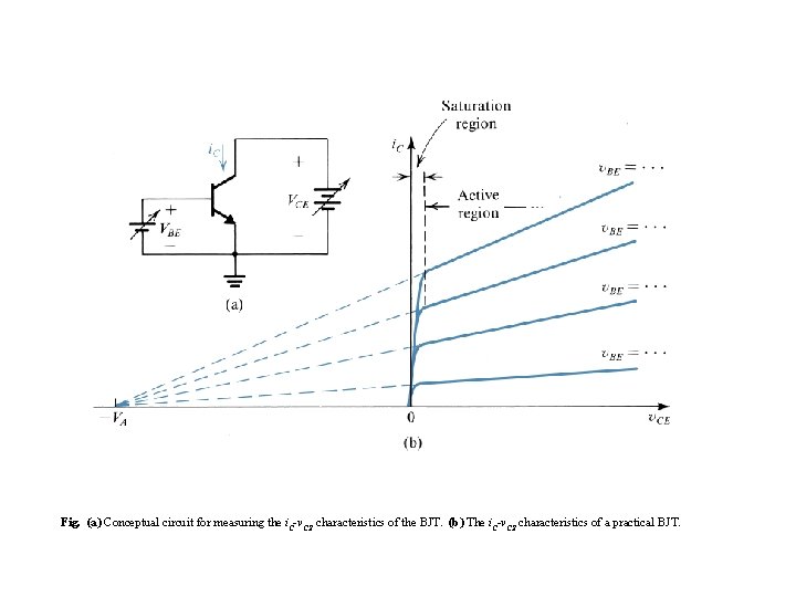
Fig. (a) Conceptual circuit for measuring the i. C-v. CE characteristics of the BJT. (b) The i. C-v. CE characteristics of a practical BJT.

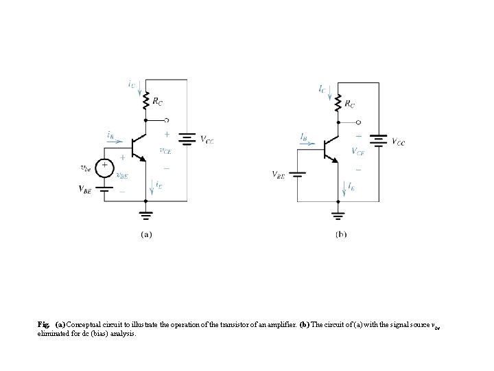
Fig. (a) Conceptual circuit to illustrate the operation of the transistor of an amplifier. (b) The circuit of (a) with the signal source vbe eliminated for dc (bias) analysis.

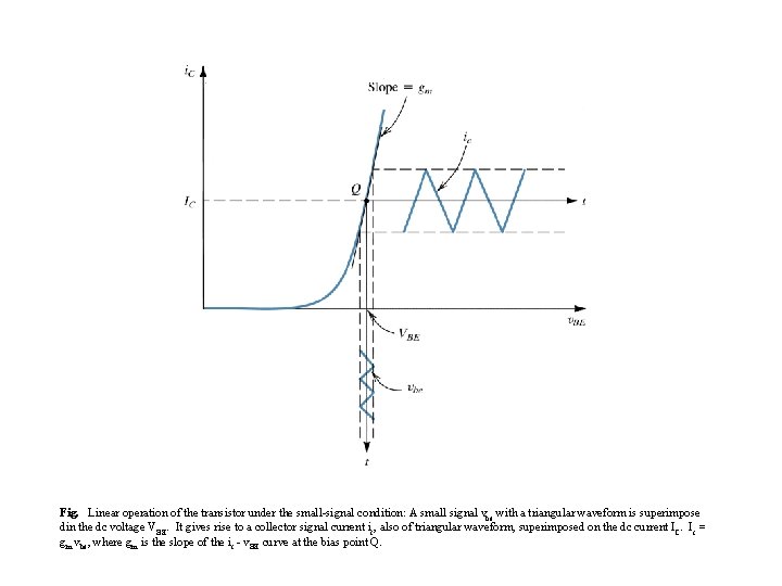
Fig. Linear operation of the transistor under the small-signal condition: A small signal vbe with a triangular waveform is superimpose din the dc voltage VBE. It gives rise to a collector signal current ic, also of triangular waveform, superimposed on the dc current IC. Ic = gm vbe, where gm is the slope of the ic - v. BE curve at the bias point Q.

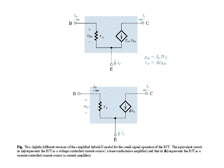
Fig. Two slightly different versions of the simplified hybrid- model for the small-signal operation of the BJT. The equivalent circuit in (a) represents the BJT as a voltage-controlled current source ( a transconductance amplifier) and that in (b) represents the BJT as a current-controlled current source (a current amplifier).

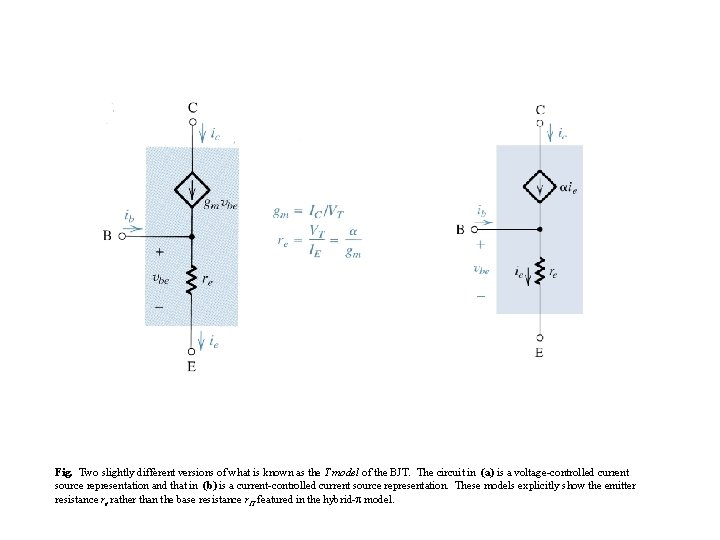
Fig. Two slightly different versions of what is known as the T model of the BJT. The circuit in (a) is a voltage-controlled current source representation and that in (b) is a current-controlled current source representation. These models explicitly show the emitter resistance re rather than the base resistance r featured in the hybrid- model.

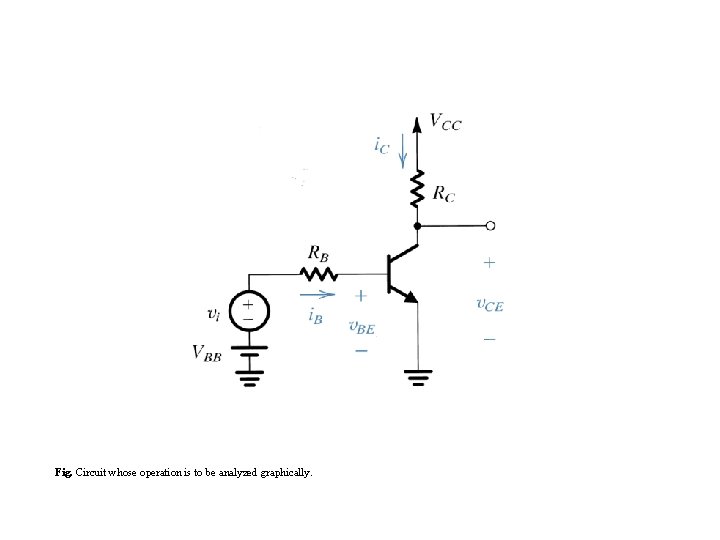
Fig. Circuit whose operation is to be analyzed graphically.

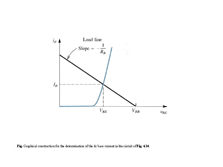
Fig. Graphical construction for the determination of the dc base current in the circuit of Fig. 4. 34.

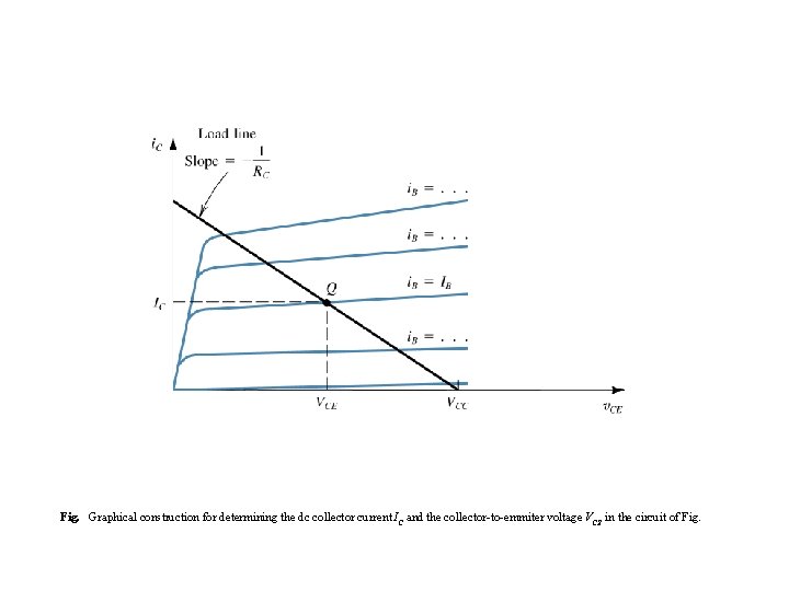
Fig. Graphical construction for determining the dc collector current IC and the collector-to-emmiter voltage VCE in the circuit of Fig.

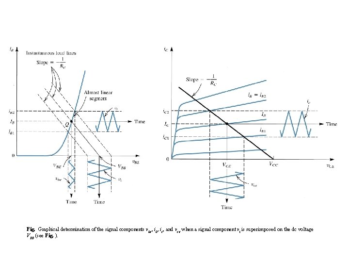
Fig. Graphical determination of the signal components vbe, ib, ic, and vce when a signal component vi is superimposed on the dc voltage VBB (see Fig. ).

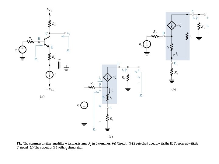
Fig. The common-emitter amplifier with a resistance Re in the emitter. (a) Circuit. (b) Equivalent circuit with the BJT replaced with its T model (c) The circuit in (b) with ro eliminated.

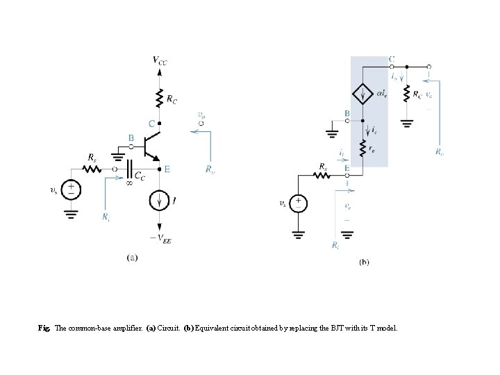
Fig. The common-base amplifier. (a) Circuit. (b) Equivalent circuit obtained by replacing the BJT with its T model.

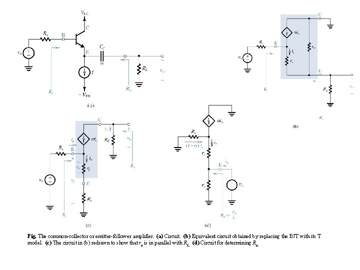
Fig. The common-collector or emitter-follower amplifier. (a) Circuit. (b) Equivalent circuit obtained by replacing the BJT with its T model. (c) The circuit in (b) redrawn to show that ro is in parallel with RL. (d) Circuit for determining Ro.

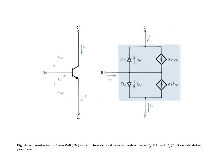
Fig. An npn resistor and its Ebers-Moll (EM) model. The scale or saturation currents of diodes DE (EBJ) and DC (CBJ) are indicated in parentheses.

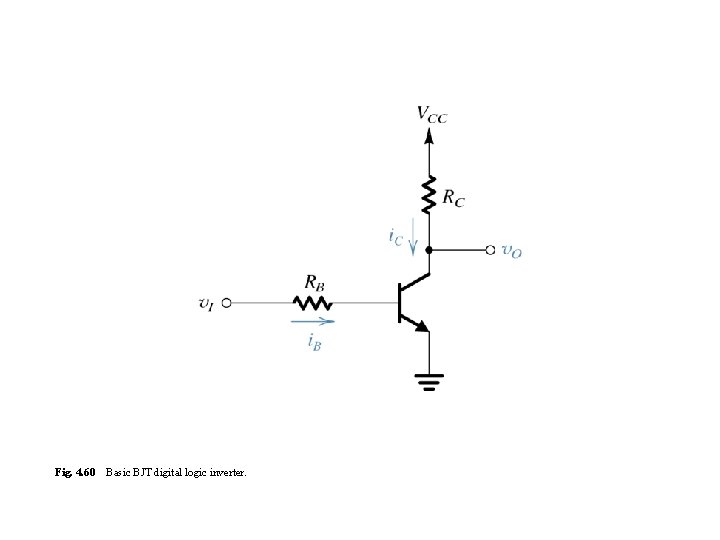
Fig. 4. 60 Basic BJT digital logic inverter.

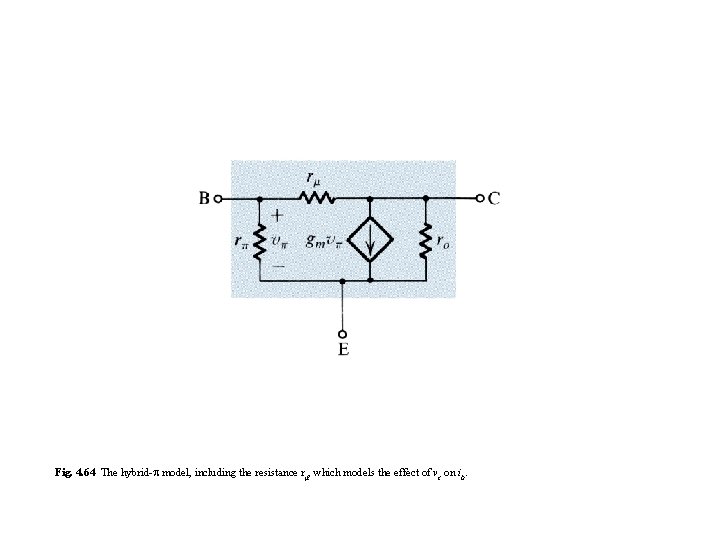
Fig. 4. 64 The hybrid- model, including the resistance r , which models the effect of vc on ib.