https www autodesk comeagle We will be using

https: //www. autodesk. com/eagle We will be using the latest!

@technolomaniac github: sfgit hackaday. io/matt Email: technolomaniac@gmail. com matt. berggren@autodesk. com

Physicist Electrical Engineer Embedded SW Developer -ish Radio / Wireless Junkie >Trying to change the world< …I build stuff (a LOT of stuff) And I wish I was a mathematician

Radios / RF Transceivers Sensors & Control Stuff Connected Hardware, Software, & Services VERY High Precision “Detectors” Electronics Design Software Modular Electronics / Development Hardware

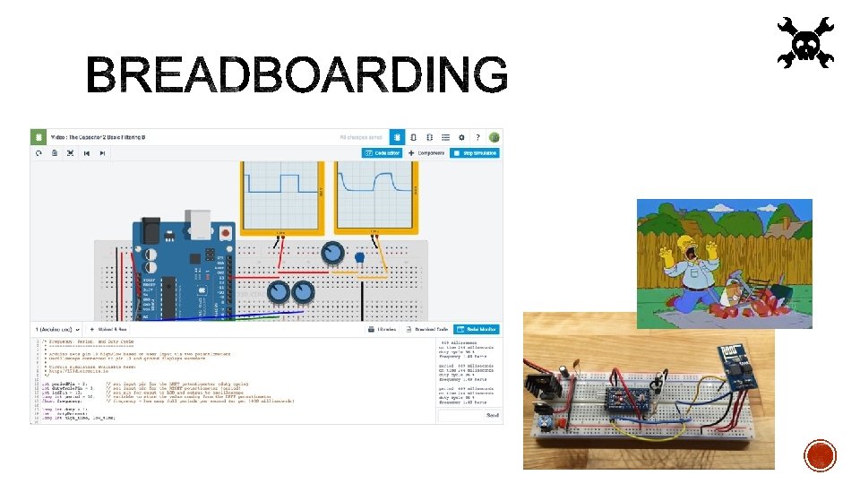
Figure 1. Modeling ideas with breadboard, prototype board and development kits
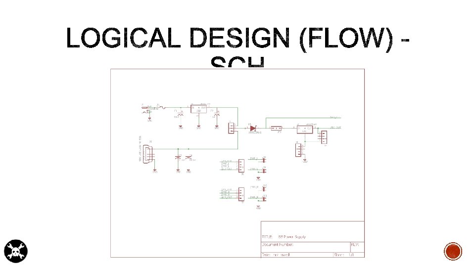
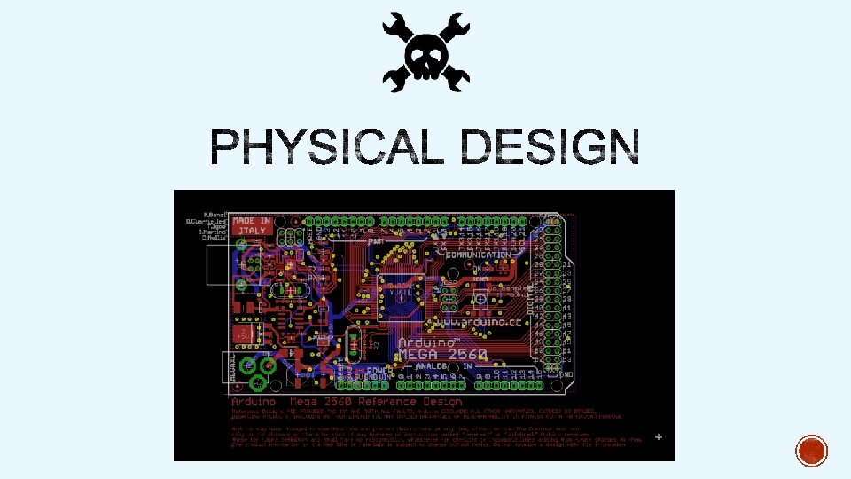

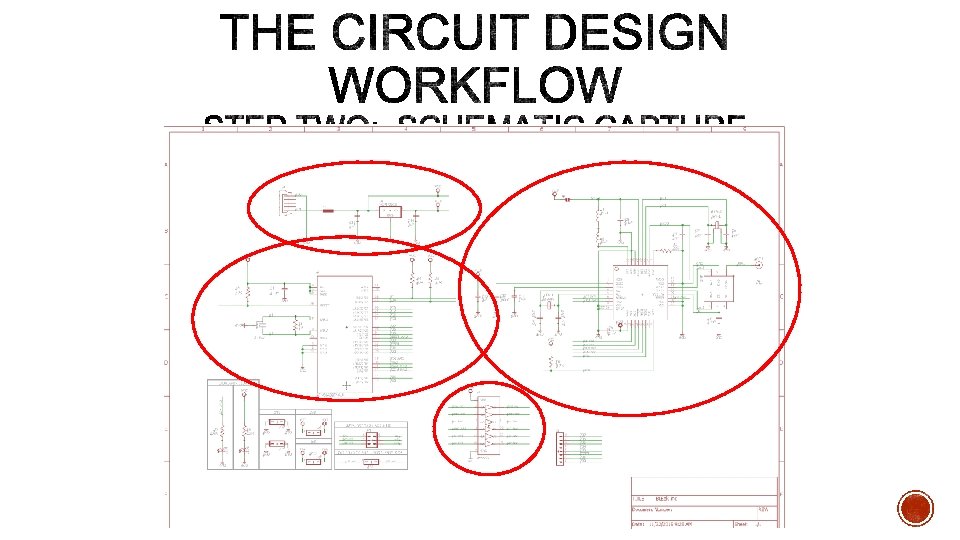
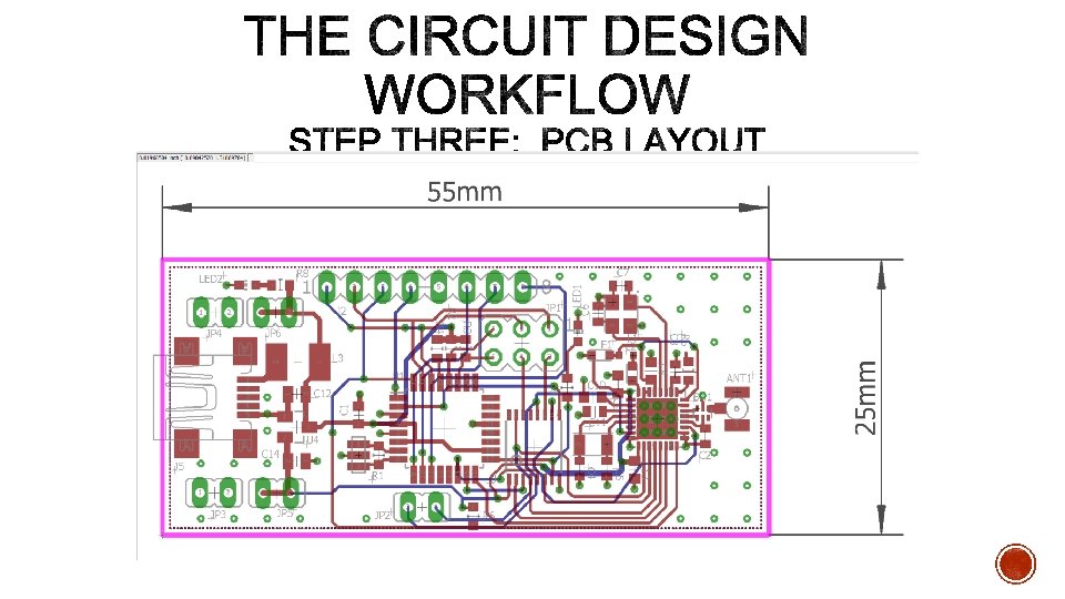
Conceptualization Schematic Capture PCB Layout Computer Aided Manufacturing


PRE-CLAD COPPER CIRCUIT BOARD PANEL
 Figure 3. Circuit")
Routed Boards No Components, No Mask (i. e. the green stuff) Figure 3. Circuit routed from preclad PCB material


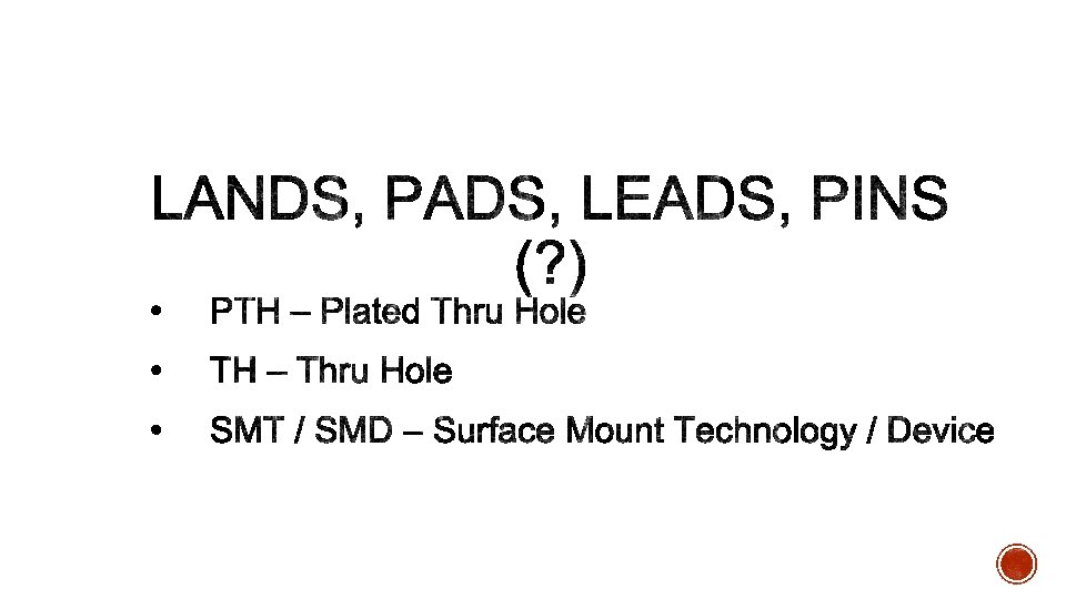
Some basic PCB terminology

Figure 5. All the same part, different “packaging”
 resting on surface mount pads on the top")
Figure 6. Component pins (gullwing leads) resting on surface mount pads on the top layer of a PCB

Figure 7. Thru-hole pad with annular rings take solder on the top and bottom layers and a plated hole

Figure 7. Cross section of a printed circuit board

Figure 8. Component pins make contact with slightly larger pads on the top layer of the PCB board


Figure 9. Signal layer with tracks and vias


Figure 10. Layer by layer view of a printed circuit board

*More common Figure 11. Layer stackup of a typical 4 layer board


Figure 12. PCB Soldermask


Figure 12. PCB File Paste Mask and Bottom Copper Layers Figure 13. PCB Solder Paste Stencil


Conceptualization Schematic Capture PCB Layout Computer Aided Manfuacturing

NRF 24 L 01

NRF 24 L 01

Storage Control Comms Intelligence Sensing Power Interface

Gerber Flattened out, layer by layer artwork of the PCB presented as flashes and draws (apertures) using D-Codes, Loc, etc NC Drilling / milling information including tools, locations, and route paths (plunge points, extraction points, etc) Bill of Materials (BOM) Pick and Place File IPC-D-356 Netlist Component, fully-qualified part numbers, quantities, manufacturers, distributor(s), equivalents (FFF), alternatives Component part numbers, X: Y locations, orientations, board layer (top or bottom) Testpoint report including testpoint location (usually pads or vias), net name

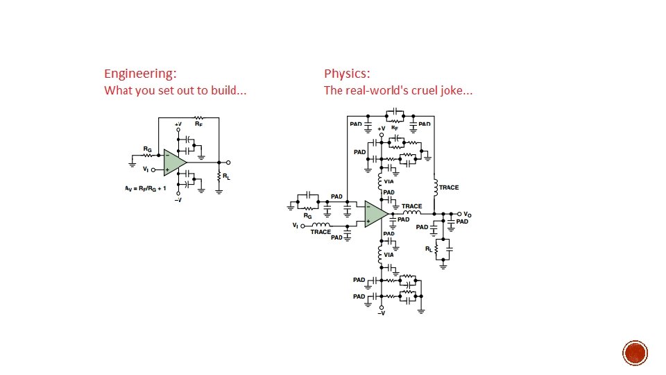

§ § § § Copper is NOT a super conductor, nor is solder Cu cannot carry infinite amounts of current Pads have to be solderable! Must work on the assembly line PCB traces have resistance, impedance, inductance Pins and pads have capacitance, impedance Vias are inductive, capacitive Coupling occurs between tracks, polygons, planes, etc. Noise propagates along signal paths, ground planes Amplifiers amplify Digital signals / components are noisy… …Analog circuitry is susceptible to noise! Antennas hear it all Remember your R’L’G’C’s (*ok, this is pretty engineering heavy) Gaaaaaahhhhh! …YET we manage to build stuff that works every day, so chill


A A 1 K 2 K SYMBOL 1 2 PACKAGE

§ Group pins meaningfully § Consider wiring of the schematic § Consider flow of design § Traditional model § Power pins top, ground bottom* § Inputs left, outputs right § Pull ups pull up § Pull downs pull down § Clock pins need space § Make room for decoupling § Save space for series resistors

§ It comes down to pad geometry and silkscreen! § IPC-7351 defines standards for land pattern & includes 3 rd party calculator for component pad geometry § Some silkscreen tips: § Silkscreen line width 10 mils (play it safe) § Ensure silkscreen is visible from beneath the component (no point adding silkscreen under a part, can be problematic) § Ensure silkscreen boundary is wide enough to accommodate comp drift § Orientation details are critical § Direction, polarity (LEDs, polarized caps) § Pin-one markers (every IC should have a dot)

§ Fall into one of two categories: thru-hole or surface mount § Pads are consistently larger than the component pin § Gullwing pads have a toe, a heel and a side, where other square pads have may have equally sized sides § Pads can extend outside of the body of the component, or leads may not be visible when components are mounted
 § § § should be")
§ SOIC and leaded gullwing pads (e. g. QFP) § § § should be oblong, rounded-rectangles Mark “Pin 1” with a square pad and a silkscreen dot beside it for clarity Thru-hole pads are general circular though pins are commonly square or rectangular, ensure room to fit pins (include plating thickness in calculations) SOT packages (e. g. LDOs, transistors) use square pads, rectangular Leadless packages incl. QFNs, diodes, etc. commonly use square pads and vias for thermal relief Discrete SMTs (resistors, caps) use square pads Ball Grid Array (BGA) packages use round pads

Pad Dimensions Package Dimensions

§ Using Rounded Surface Mount Lands § Clean release from solder paste stencil § Reduces solder volume § A more natural shape for solder in its liquid form § Concentrates solder where it is most needed § Rule of thumb -> take nominal pad size and add 40 mils to length (20 toe, 20 heel) § Rule of thumb -> take nominal pad size and: § Pitch = 50 mils, add 10 mils to the width § Pitch = 0. 8 mm, use 20 mils wide pads § Pitch = 0. 65 mm, use 16 mils wide pads § Pitch = 0. 5 mm, use 14 mils wide pads

 §")
§ The world loves little cities…hates urban sprawl (don’t be LA, be Shanghai) § Group analog and digital circuits into separate sections § Keep sections (power, MCU, transceiver, analog, etc) tight though maintain enough room for soldering, esp. if soldering by hand § Watch the tall parts vs. short parts and don’t paint yourself into a corner when hand-soldering (can’t reach something) § Components slip when soldering (float), keep parts >10 mils apart for machine assembly and >20 for hand assembly unless you have serious soldering chops § Keep decoupling to w/in a min of 100 mil of the component pins, 50 mil is better § Keep analog circuits close to the board’s IO § Keep components 150 mils from the edge of the board so clamps can be used

 § Current carrying capacity §")
Power Supply -> Far more scientific…based on ampacity (current) § Current carrying capacity § Temperature Rise § Thickness of copper § Width of the track § Current requirements IPC 2221 Formula: i=K×∆T 0. 44×Ac 0. 725 Where: i = required current K = 0. 048 for external layers 0. 024 for internal layers ∆T = temp rise in o. C Ac = cross sectional area (width x thickness)

12 mil Power Supply -> Some rules of thumb § Base your routing width on 1. 5 -2 x the required current § Use planes whenever possible § Avoid long return paths, shorter is better, best = via to solid plane § Avoid long unterminated stubs (antennae)* § Give yourself meaningful clearance between traces § “Neck Down” tracks to enter pads at pad width or slightly smaller § Avoid splitting power and ground on the same layer § Avoid digital signals over analog ground planes (more on this) * Straight conductors (unterminated) have parasitic inductance and concentrate flux lines (magnetics) from the world around them…this is the principle of a whip antenna and straight, unterminated tracks can operate like antennas on the board concentrating noise and introducing it to a circuit 15 mil 20 mil 25 mil 30 mil

§ Regarded as the noisy bunch, though reasonably noise-immune themselves § Should be kept as short as possible to avoid parading noise around the board § Should be kept away from sensitive analog signals where possible and avoid crossing analog GND planes § Run orthogonal on adjacent layers to limit crosstalk and noise issues § Isolate digital ground from analog ground wherever possible* *does not apply to ADCs and DACs…a DACs DGND and AGND pins should both be tied to AGND plane as close to the component as possible →→→→→
 Some rules of thumb §")
15 mil Digital Signals-> <= Scientific (High speed excepted) Some rules of thumb § As trace width decreases, resistance increases § As length increases, so does resistance 12 mil 10 mil § As trace width increases, capacitance (particularly with the presence of a GND plane) increases § Under most non-RF or non-”High Speed” circumstances, it is aesthetics and cost (PCB fab) that drive this - W < 5 mil = ↑$. . . § Typical track widths: 5, 7, 8, 10, 12, 15, 20, 25, 50… § You can use larger tracks to make life simpler 7 mil 5 mil

15 mil Digital Signals-> Some rules of thumb § Wider traces are easier to etch chemically and route with a § § § CNC machine Building in-house prototypes, look for 15 mil tracks and 15 mil spacing min. unless using a precision mill Chemical etch can be hard to time right, unpredictable, good to “go big” PCB manufacturer’s can reliably handle 5 mil tracks and 5 mil spacing (so-called 5 x 5) Larger tracks / spacing = better yield = lower cost Don’t overdo it…no one likes and overachiever when it comes to track width (don’t waste space) Super-wide tracks introduce additional capacitance, can be problematic in higher speed circuits 12 mil 10 mil 7 mil 5 mil

Ex. Sunstone Circuits Selecting a via size for “typical” circuits § Most low-cost fabs will require >= 15 mil via holes § Full service board houses will provide sizes much smaller but typically charge more for <= 12 mil diameter § Aim for 1. 8 x-2. 0 x hole diameter for annular ring size § Manufacturer’s will “round” to their nearest size and all mfg will have a standard size they recommend / prefer

Power Supply -> Some rules of thumb § IPC-9592 specifies that for voltages. >= 100 V, the formula for minimum clearance vs. voltage to be (linear): SPACING (mm) = 0. 6 + Vpeak x. 005 § For voltages < 100 V the formula is: 0. 13 mm for V<15 V 0. 25 mm for 15 V≤V<30 V 0. 1+Vpeak× 0. 01 for 30 V≤V<100 V § Larger clearances are better and a nice rule of thumb is to allow clearance to match track width for most low-voltage circuits (for power): 20 mil track x 20 mil spacing § RULE: Don’t follow this chart…this is a minimum…maintain a minimum of 10 mils clearance for low power nets and life will be good (most of the time: )

 § Greater")
§ Power lines should be kept to the lowest possible impedance √(L/C) § Greater width = lower impedance, Single GND, Shared Return Path thicker copper = lower impedance § Long power lines couple in more noise from other parts of the circuit and parade that noise everywhere they go…keep @%^& short and isolate! Multiple returns, shared return path Multiple returns, isolated return paths

§ Ground planes should be unbroken where possible § Ground planes should not be mixed with Single GND, Shared Return Path power or other signals where possible § Route digital signals *around* analog ground planes § Isolate returns whenever possible (nobody likes the noisemakers at the party) Multiple returns, shared return path Multiple returns, isolated return paths
 § Designed to remove ambiguity with SMT parts")
§ Follow the IPC Specifications (IPC-7351) § Designed to remove ambiguity with SMT parts handling and PCB land-pattern geometries § Comes with IPC Footprint Calculator § Refer to IPC-7351 tables 3. 1 – 3. 22 § Join forums like www. pcblibraries. com or the IPC designer’s council forum § Manufacturers will be able to tell you minimum / recommended annular ring on thru-hole pads § Get samples, print the design 1: 1 and have a look…May not tell you it’s mfg-worthy but will tell you if the overall size is completely wrong § Pay careful attention to pad numbering § Never obscure pads with silkscreen or anything else § Ask, ask…Average the answers : ) …And (note to self) always tent the vias under your BGAs
 § Search")
§ IPC 2221 (Free online…you’ll find a PDF, just have a copy) § Search – PCB Pad Size, PCB Footprint Size, PCB Land Pattern § IPC 2152 – like 2221 but more accurate and § Saturn PCB calculator – you want this more use of tables § IPC 7351 – buy this little jewel…it may be pricey but it’s worth it § Join forums: § Electronics Exchange § All About Circuits § PCBLibraries. com § IPC Designer’s Council § App. CAD PCB – you want this § PCB Library Expert Lite – Free, you want this…always nice to buy it if you can § Read the books from the American Radio and Relay League § US Navy electronics resource are decent
 § Good soldering kit – Aoyue, Weller (though specialized tips on some)")
a pen) § Good soldering kit – Aoyue, Weller (though specialized tips on some) § Multimeter § USB to serial port adapter (you will need this with great frequency) § Oscilloscope – you need to get eyes into your circuit § Logic analyzer (USB are ok…look at Saeleg, not bad, min 8 -channel) § Tweezers (Vetus brand are nice, you want decent sets of different tips, hooks are the best) § PCB circuit cleaner (spray from Radio. Shack) § A few extra tooth brushes for cleaning boards, soft tip, none of that wonky gum massage nonsense § XACTO knife with replacement blades § Wire strippers § Solid core wire (22 gauge) § Stranded wire (important to take stress off of solder joints) § Hot air setup / hotplate § Solder + flux (flux should be both a jar of paste and
- Slides: 70