VLSI System Design Lecture 1 6 Tristates Mux



- Slides: 22

VLSI System Design Lecture: 1. 6 Tri-states, Mux, Latches & Flip Flops Engr. Anees ul Husnain ( anees. buzdar@gmail. com ) Department of Computer Systems Engineering, College of Engineering & Technology, IUB

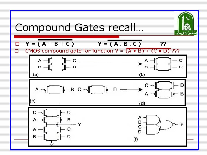
Compound Gates recall… o Y=(A+B+C) Y=(A. B. C) ? ? o CMOS compound gate for function Y = (A • B) + (C • D) ? ? ?

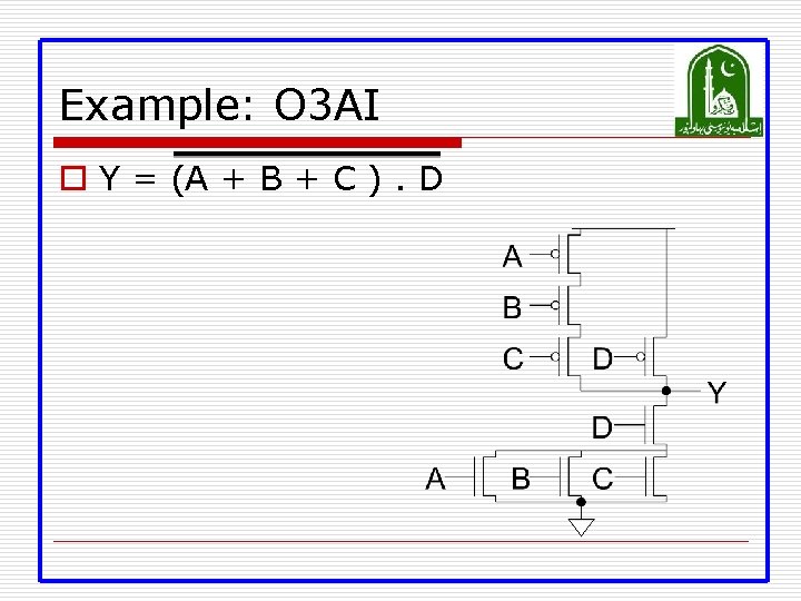
Example: O 3 AI o Y = (A + B + C ). D

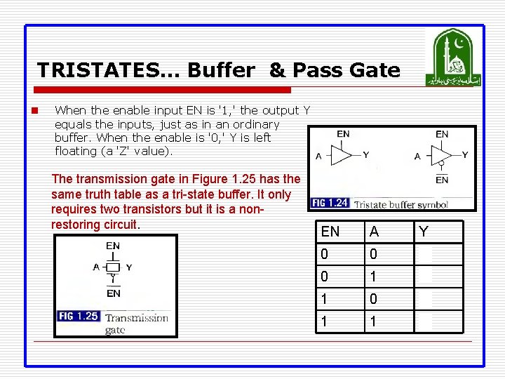
TRISTATES… Buffer & Pass Gate n When the enable input EN is '1, ' the output Y equals the inputs, just as in an ordinary buffer. When the enable is '0, ' Y is left floating (a 'Z' value). The transmission gate in Figure 1. 25 has the same truth table as a tri-state buffer. It only requires two transistors but it is a nonrestoring circuit. EN A Y 0 0 Z 0 1 Z 1 0 0 1 1 1

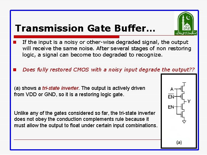
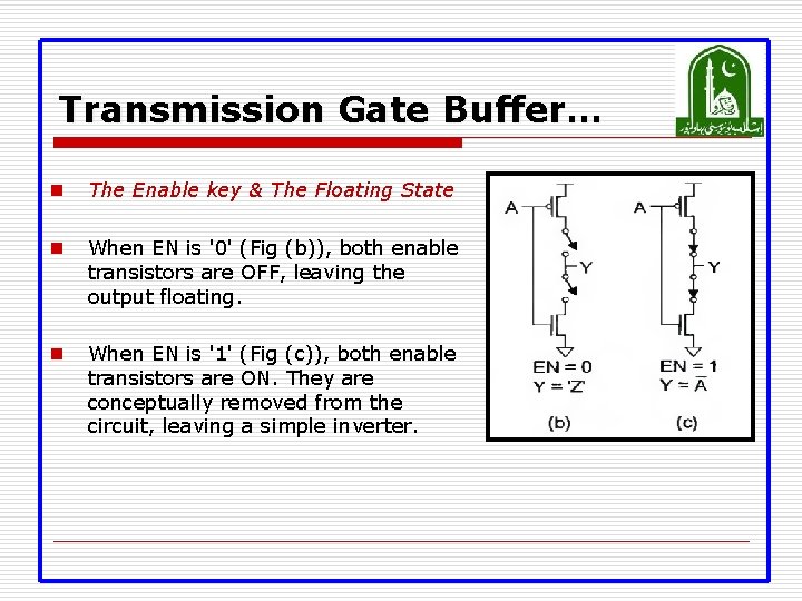
Transmission Gate Buffer… n If the input is a noisy or other-wise degraded signal, the output will receive the same noise. After several stages of non restoring logic, a signal can become too degraded to recognize. n Does fully restored CMOS with a noisy input degrade the output? ? (a) shows a tri-state inverter. The output is actively driven from VDD or GND, so it is a restoring logic gate. Unlike any of the gates considered so far, the tri-state inverter does not obey the conduction complements rule because it must allow the output to float under certain input combinations.

Transmission Gate Buffer… n The Enable key & The Floating State n When EN is '0' (Fig (b)), both enable transistors are OFF, leaving the output floating. n When EN is '1' (Fig (c)), both enable transistors are ON. They are conceptually removed from the circuit, leaving a simple inverter.

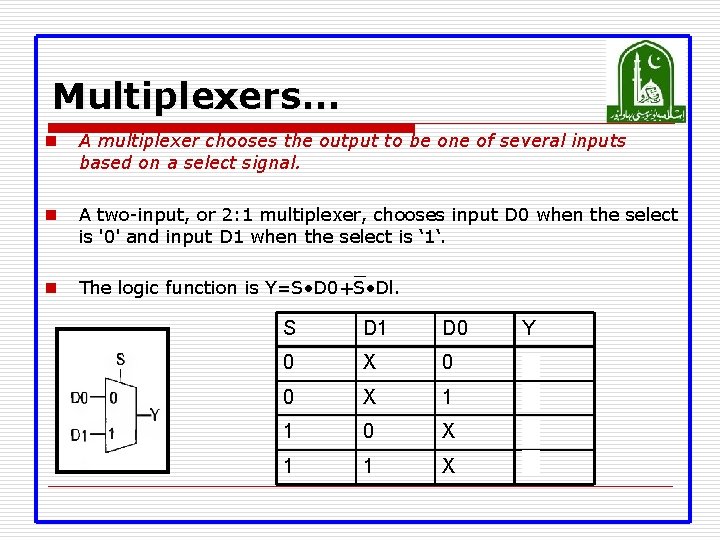
Multiplexers… n A multiplexer chooses the output to be one of several inputs based on a select signal. n A two-input, or 2: 1 multiplexer, chooses input D 0 when the select is '0' and input D 1 when the select is ‘ 1‘. n The logic function is Y=S • D 0+S • Dl. S D 1 D 0 Y 0 X 0 0 0 X 1 1 1 0 X 0 1 1 X 1

Gate-Level Multiplexer Design o o How many transistors are needed? 20

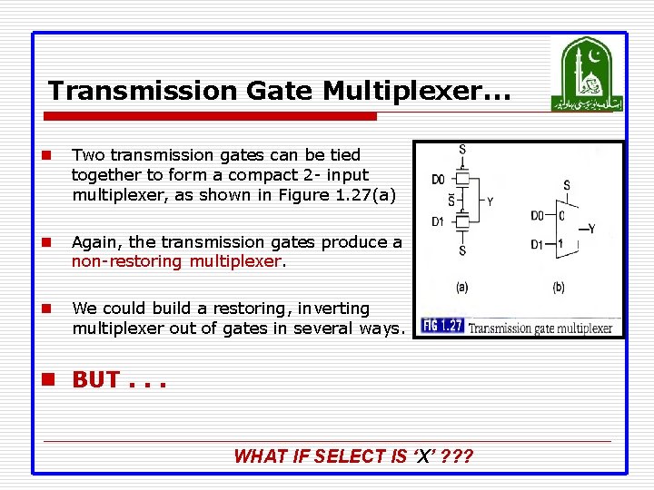
Transmission Gate Multiplexer… n Two transmission gates can be tied together to form a compact 2 - input multiplexer, as shown in Figure 1. 27(a) n Again, the transmission gates produce a non-restoring multiplexer. n We could build a restoring, inverting multiplexer out of gates in several ways. n BUT. . . WHAT IF SELECT IS ‘X’ ? ? ?

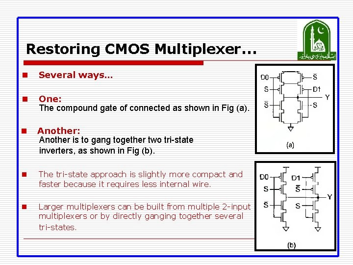
Restoring CMOS Multiplexer… n Several ways… n One: The compound gate of connected as shown in Fig (a). n Another: Another is to gang together two tri-state inverters, as shown in Fig (b). n The tri-state approach is slightly more compact and faster because it requires less internal wire. n Larger multiplexers can be built from multiple 2 -input multiplexers or by directly ganging together several tri-states.

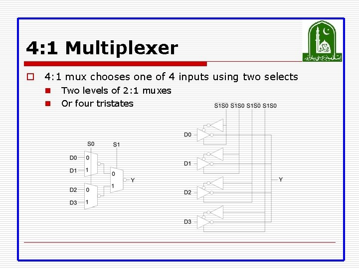
4: 1 Multiplexer o 4: 1 mux chooses one of 4 inputs using two selects n n Two levels of 2: 1 muxes Or four tristates

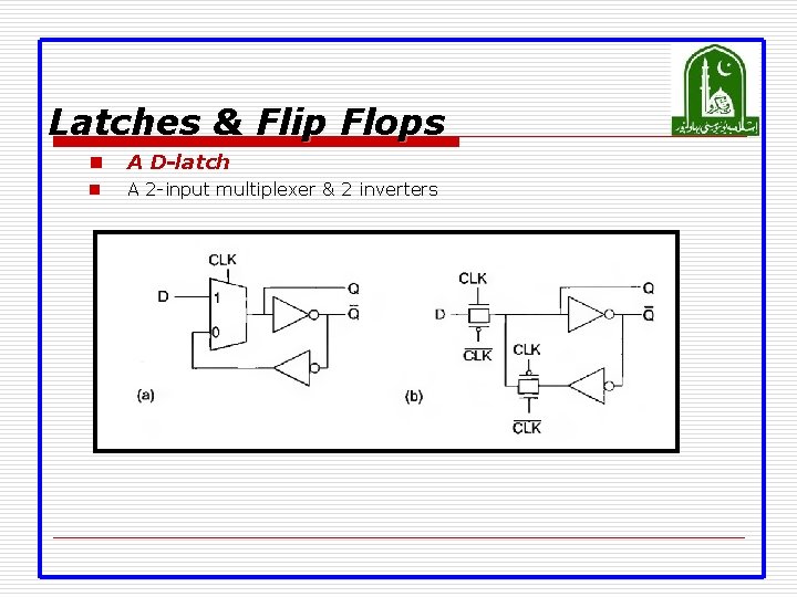
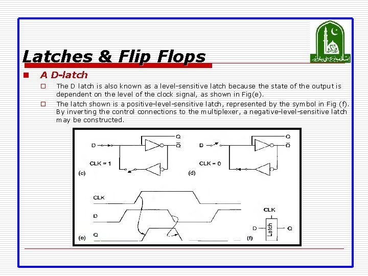
Latches & Flip Flops n A D-latch n A 2 -input multiplexer & 2 inverters

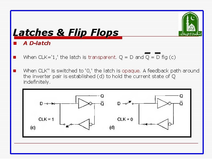
Latches & Flip Flops n A D-latch n When CLK=‘ 1, ' the latch is transparent. Q = D and Q = D fig (c) n When CLK" is switched to '0, ' the latch is opaque. A feedback path around the inverter pair is established (d) to hold the current state of Q indefinitely.

Latches & Flip Flops n A D-latch o o The D latch is also known as a level-sensitive latch because the state of the output is dependent on the level of the clock signal, as shown in Fig(e). The latch shown is a positive-level-sensitive latch, represented by the symbol in Fig (f). By inverting the control connections to the multiplexer, a negative-level-sensitive latch may be constructed.

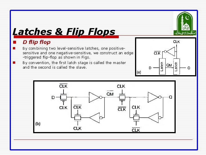
Latches & Flip Flops n D flip flop n By combining two level-sensitive latches, one positivesensitive and one negative-sensitive, we construct an edge -triggered flip-flop as shown in Figs. By convention, the first latch stage is called the master and the second is called the slave. n

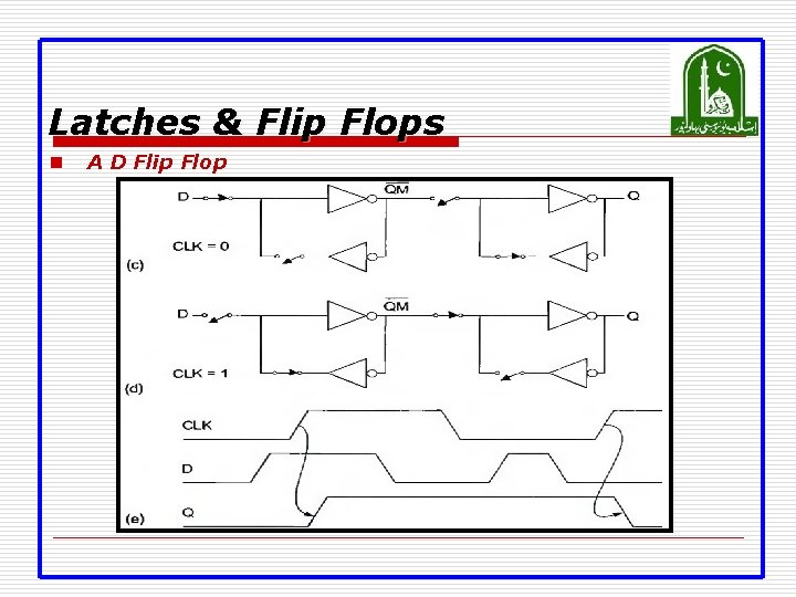
Latches & Flip Flops n A D Flip Flop o o While CLK is low, the master negative-level-sensitive latch output (QM) follows the D input while the slave positive-level-sensitive latch holds the previous value (Fig(c)). When the clock transitions from 0 to 1, the master latch ceases to sample the input and holds the D value at the time of the clock transition.

Latches & Flip Flops n A D Flip Flop

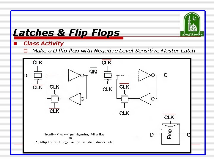
Latches & Flip Flops n Class Activity o Make a D flip flop with Negative Level Sensitive Master Latch

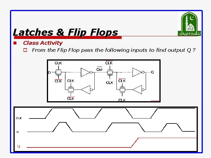
Latches & Flip Flops n Class Activity o From the Flip Flop pass the following inputs to find output Q ?

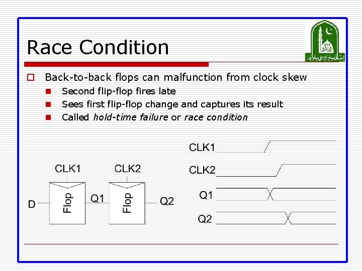
Race Condition o Back-to-back flops can malfunction from clock skew n n n Second flip-flop fires late Sees first flip-flop change and captures its result Called hold-time failure or race condition

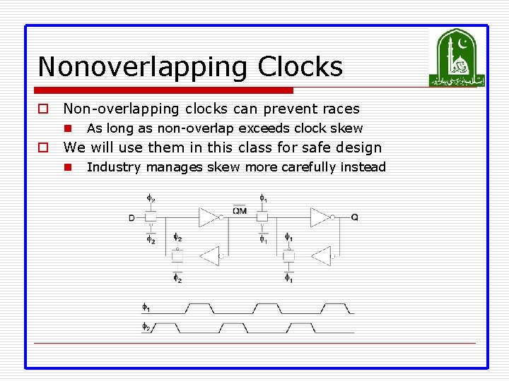
Nonoverlapping Clocks o Non-overlapping clocks can prevent races n As long as non-overlap exceeds clock skew o We will use them in this class for safe design n Industry manages skew more carefully instead

Next… o Layout Design o Stick Diagrams