SOLAR CELLS Dr Mohammad Aminul Islam Assistant Professor

 solar array Types")


 Solar array Single solar cell • sandwiched with p-type")

 solar array (or) Solar module The solar panel (or) solar array")


 Monocrystalline silicon 14 -17 Polycrystalline")


")


 Carbon (nanotubes,")

 has")


 : A Review")


- Slides: 72
SOLAR CELLS Dr. Mohammad Aminul Islam Assistant Professor Dept. of Electrical & Electronic Engineering International Islamic University Chittagong M A Islam, EEE, IIUC 1
Lecture Outline Introduction Photovoltaic effect Electron-hole formation A solar panel (or) solar array Types of Solar cell Principle, construction and working of Solar cell Advantage, disadvantage and application M A Islam, EEE, IIUC 2
OUTLINE o Solar cell fundamentals o Requirements for an ideal solar cell o Thin film materials for viable solar cells o Strengths and Weaknesses of various thin film cells o Comparative production status of various cells o New concepts to enhance cell conversion efficiency o Concluding Remarks 3
1. Introduction Recap : Photo means light in Greek and Volt is the name of a pioneer in the study of electricity Alessandro Volta Albert Einstein was awarded the 1921 Nobel Prize in physics for his research on the photoelectric effect—a phenomenon central to the generation of electricity through solar cells. In the early stages, the solar cell was developed only with 4 to 6 % efficiency( because of inadequate materials and problems in focusing the solar radiations). But, after 1989, the solar cells with more than 50% efficiency was developed. M A Islam, EEE, IIUC 4
Three generations of solar cells First Generation First generation cells consist of large-area, high quality and single junction devices. First Generation technologies involve high energy and labour inputs which prevent any significant progress in reducing production costs. M A Islam, EEE, IIUC 5
Second Generation Second generation materials have been developed to address energy requirements and production costs of solar cells. Alternative manufacturing techniques such as vapour deposition and electroplating are advantageous as they reduce high temperature processing significantly M A Islam, EEE, IIUC 6
Materials for Solar cells are composed of various semiconducting materials 1. 2. 3. 4. 5. 6. Crystalline silicon Cadmium telluride Copper indium diselenide Gallium arsenide Indium phosphide Zinc sulphide Note: Semiconductors are materials, which become electrically conductive when supplied with light or heat, but which operate as insulators at low temperatures M A Islam, EEE, IIUC 7
• M A Islam, EEE, IIUC 8
• If two differently contaminated semiconductor layers are combined, then a so-called p-n-junction results on the boundary of the layers. p-n junction layer n-type semiconductor p- type semiconductor • By doping trivalent element, we get p-type semiconductor. (with excess amount of hole) • By doping pentavalent element, we get semiconductor ( with excess amount of electron) M A Islam, EEE, IIUC n-type 9
2. Photovoltaic effect Definition: The generation of voltage across the PN junction in a semiconductor due to the absorption of light radiation is called photovoltaic effect. The Devices based on this effect is called photovoltaic device. Light energy n-type semiconductor p- type semiconductor Electrical Power p-n junction M A Islam, EEE, IIUC 10
Solar cell – Working Principle l Operating diode in fourth quadrant generates power
3. electron-hole formation Photovoltaic onversion relies energy • of photons strikes on the earth. (photon is a flux of light particles) • square second. centimeter of the Earth's surface every • excess of the band gap - can be converted into electricity by the solar cell. • be absorbed and promote an electron from the valence band to the conduction band. M A Islam, EEE, IIUC 12
Conduction band electron Photons hole Valence band ore, • is called hole. • valence band combine together and forms electron-hole pairs. M A Islam, EEE, IIUC 13
4. A solar panel (or) Solar array Single solar cell • sandwiched with p-type layer. • large-area p-n junction made from silicon wafer. • electricity • a calculator. • electronic appliances such as watches and calculators M A Islam, EEE, IIUC 14
Single Solar cell N-type P-type M A Islam, EEE, IIUC 15
Solar panel (or) solar array (or) Solar module The solar panel (or) solar array is the interconnection of number of solar module to get efficient power. • solar cells. • glass plate to protect from the bad whether. • can be produced. M A Islam, EEE, IIUC 16
M A Islam, EEE, IIUC 17
5. Types of Si Solar cell Based on the types of crystal used, soar cells can be classified as, 1. Monocrystalline silicon cells 2. Polycrystalline silicon cells 3. Amorphous silicon cells 1. The Monocrystalline silicon cell is produced from pure silicon (single crystal). Since the Monocrystalline silicon is pure and defect free, the efficiency of cell will be higher. 2. In polycrystalline solar cell, liquid silicon is used as raw material and polycrystalline silicon was obtained followed by solidification process. The materials contain various crystalline sizes. Hence, the efficiency of this type of cell is less than Monocrystalline cell. M A Islam, EEE, IIUC 18
3. Amorphous silicon was obtained by depositing silicon film on the substrate like glass plate. • The layer thickness amounts to less than 1µm – the thickness of a human hair for comparison is 50 -100 µm. • The efficiency of amorphous cells is much lower than that of the other two cell types. • As a result, they are used mainly in low power calculators, pocket equipment, watches andassuch or as facade elements. M A Islam, EEE, IIUC 19
Comparison of Types of solar cell Material Efficiency (%) Monocrystalline silicon 14 -17 Polycrystalline silicon 13 -15 Amorphous silicon 5 -7 M A Islam, EEE, IIUC 20
6. Principle, construction and working of Solar cell Principle: of photovoltaic effect. The photovoltaic effect is the photogeneration of charge carriers in a light absorbing materials as a result of absorption of light radiation. Construction • semiconductor (emitter) layer and p-type semiconductor layer (base). The two layers are sandwiched and hence there is formation of p-n junction. e • the loss of incident light energy due to reflection. M A Islam, EEE, IIUC 21
M A Islam, EEE, IIUC 22
M A Islam, EEE, IIUC 23
• proper A metal contacts are made on the n-type and ptype side of the semiconductor for electrical connection Working: • energies are absorbed by a semiconduction materials. absorded this • to Due enrgy, electrons thelibereted are and produce the external DC current. • using an inverter for different applications. M A Islam, EEE, IIUC 24
Mechanism: • panel. • to increase in energy. At the same time making them free move around in the material. ever, • only a short time before returning to their original lower energy position. • energy gained from the light, a PN junction is typically used. M A Islam, EEE, IIUC 25
• A PN junction consists of two different regions of a semiconductor material (usually silicon), with one side called the p type region and the other the n-type region. • During the incident of light energy, in p-type material, electrons can gain energy and move into the n-type region. • Then they can no longer go back to their original low energy position and remain at a higher energy. • The process of moving a light- generated carrier from p-type region to n-type region is called collection. • These collections of carriers (electrons) can be either extracted from the device to give a current, or it can remain in the device and gives rise to a voltage. M A Islam, EEE, IIUC 26
• up their energy to whatever is connected to the solar cell, and then re-enter the solar cell. Once back in the solar cell, the process begins again: M A Islam, EEE, IIUC 27
The mechanism of electricity production- Different stages Conduction band High density Valence band Low density E The above diagram shows the formation of p-n junction in a solar cell. The valence band is a low-density band conduction band is high-density band. M A Islam, EEE, IIUC 28
Stage-1 When light falls on the semiconductor surface, the electron from valence band promoted to conduction band. Therefore, the hole (vacancy position left by the electron in the valence band) is generates. Hence, there is a formation of electron-hole pair on the sides of p-n junction. Conduction band High density E Valence band M A Islam, EEE, IIUC Low density 29
Stage-2 In the stage 2, the electron and holes are diffuse across the p -n junction and there is a formation of electron-hole pair. Conduction band High density junction E Valence band Low density M A Islam, EEE, IIUC 30
Stage-3 In the stage 3, As electron continuous to diffuse, the negative charge build on emitter side and positive charge build on the base side. Conduction band High density junction E Valence band Low density M A Islam, EEE, IIUC 31
Stage-4 When the PN junction is connected with external circuit, the current flows. Conduction band High density junction E Valence band Low density M A Islam, EEE, IIUC Power 32
7. Advantage, disadvantage and application of Solar cell Advantage 1. 2. 3. It is clean and non-polluting It is a renewable energy 4. 5. Solar cells do not produce noise and they are totally silent. They require very little maintenance They are long lasting sources of energy which can be 6. 7. used almost anywhere They have long life time There are no fuel costs or fuel supply problems M A Islam, EEE, IIUC 33
Disadvantage 1. Soar power can be obtained in night time 2. Soar cells (or) solar panels are very expensive 3. Energy has not be stored in batteries 4. Air pollution and whether can affect the production of electricity 5. They need large are of land to produce more efficient power supply M A Islam, EEE, IIUC 34
Applications 1. Soar pumps are used for water supply. 1. Domestic power supply for appliances include refrigeration, washing machine, television and lighting 1. Ocean navigation aids: Number of lighthouses and most buoys are powered by solar cells 1. Telecommunication systems: radio transceivers on mountain tops, or telephone boxes in the country can often be solar powered 1. Electric power generation in space: To providing electrical power to satellites in an orbit around the Earth M A Islam, EEE, IIUC 35
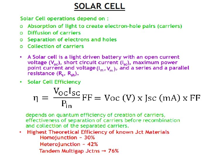
SOLAR CELL: PHOTOVOLTAICS • Direct Conversion of light into electrical energy is called PHOTOVOLTAICS (PV) • Photovoltaic devices which convert solar energy into electricity are called SOLAR CELLS • Two electronically dissimilar materials (with different free electron densities) brought together to form a junction with a barrier form a PV device. Typical examples are : �metal 1 -oxide-metal 2 �metal-semiconductor (Schottky) �p-type semiconductor-n-type semiconductor (Homojunction) �n+-n semiconductor �p-type semiconductor(1)-n-type semiconductor(2) (Heterojunction) 36
Appealing Characteristics • • Consumes no fuel No pollution Wide power-handling capabilities High power-to-weight ratio
Solar cell – Working Principle l Operating diode in fourth quadrant generates power
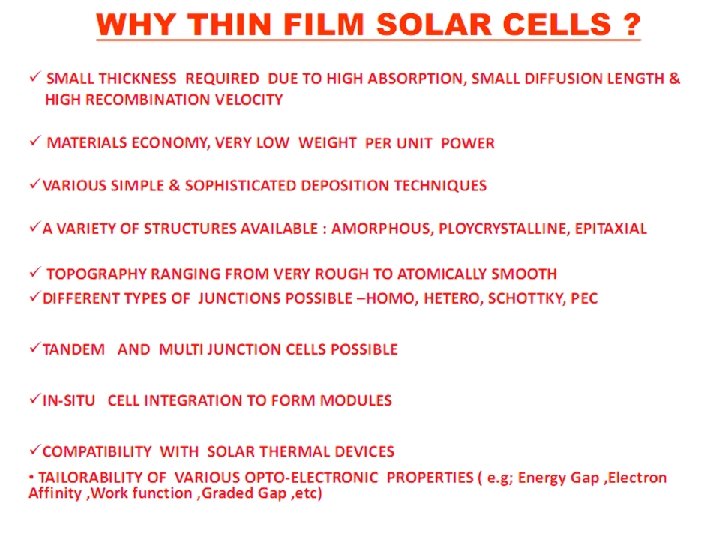
What is essential for an ideal Solar Cell 1. Cheap, Simple and Abundant Material 2. Integrated Large Scale Manufacturabilty 3. Cost (< 1$/watt)and Long Life v HIGH ABSORPTION COEFFICIENT > 105 cm-1 with direct band gap ~1. 5 e. V v JUNCTION FORMATION ABILITY v HIGH QUANTUM EFFICIENCY v LONG DIFFUSION LENGTH v LOW RECOMBINATION VELOCITY v ABUNDANT, CHEAP & ECO-FRIENDLY MATERIAL o CONVENIENCE OF SHAPES AND SIZES o SIMPLE AND INEXPENSIVE INTEGRATED PROCESSING/MANUFACTURABILITY o MINIMUM MATERIAL / WATT o MINIMUM ENERGY INPUT/ WATT o ENERGY PAY BACK PERIOD < 2 YEARS 40
Loss Processes in a Standard Solar Cell Figure: Loss processes in a standard solar cell: (1) non absorption of below bandgap photons; (2) lattice thermalization loss; (3) and (4) junction and contact voltage losses; (5) recombination loss (radiative recombination is unavoidable)
Modeled Losses in a Standard Solar Cells
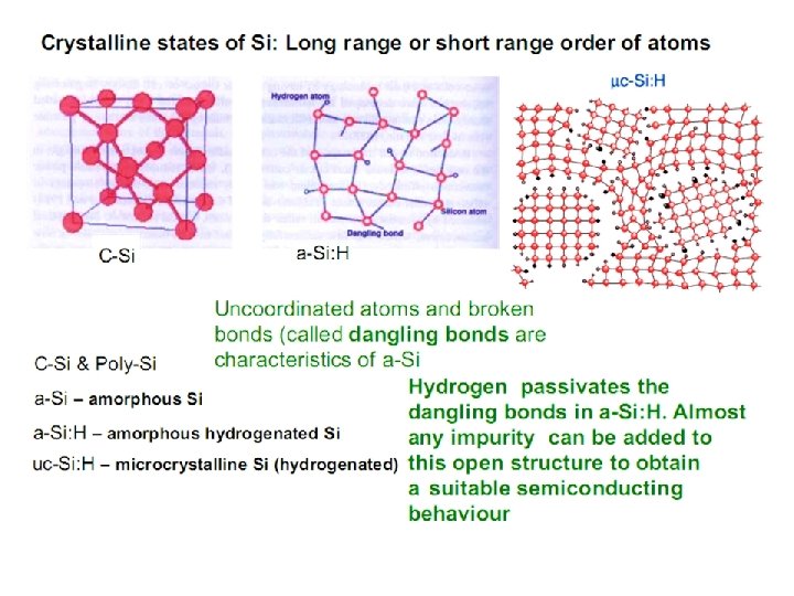
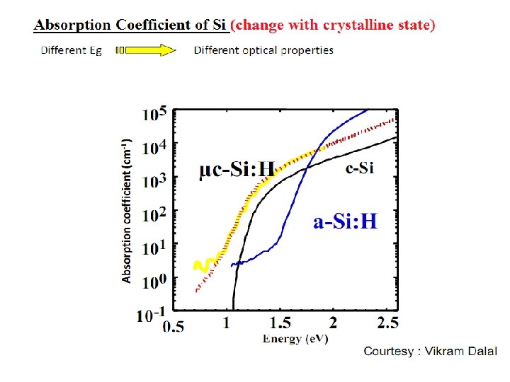
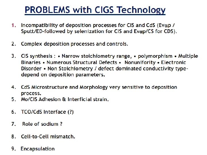
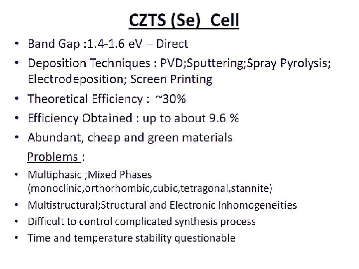
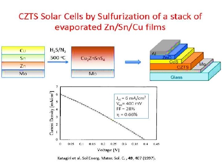
POSSIBLE SOLAR CELL MATERIALS Single Elements: Si ( bulk, mc, nc, mixed) Carbon (nanotubes, DLC) Binary alloys / Compounds: Cu 2 S, Cu 2 O Cu-C, Cd. Te, Cd. Se, Ga. P, Ga. As, In. P, Zn. P , a-Si : H, Dye coated Ti. O 2 Ternary (+) Alloys / Compounds: Cu-In-S, Cu-In-Se, Cu-Zn-S, Cd. Zn. Se , Cd. Mn. Te, Bi-Sb-S, Cu-Bi-S, Cu-Al-Te, Cu-Ga. Se, Ag-In-S, Pb-Ca-S, Ag-Ga-S, Ga-In-P, Ga-In-Sb , and so on. Organic-Inorganic Materials & Organic Materials: 43
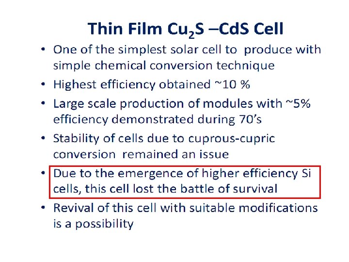
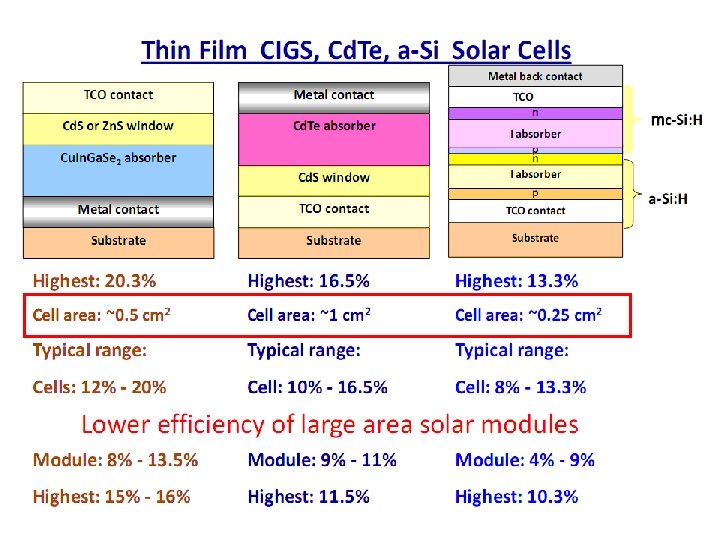
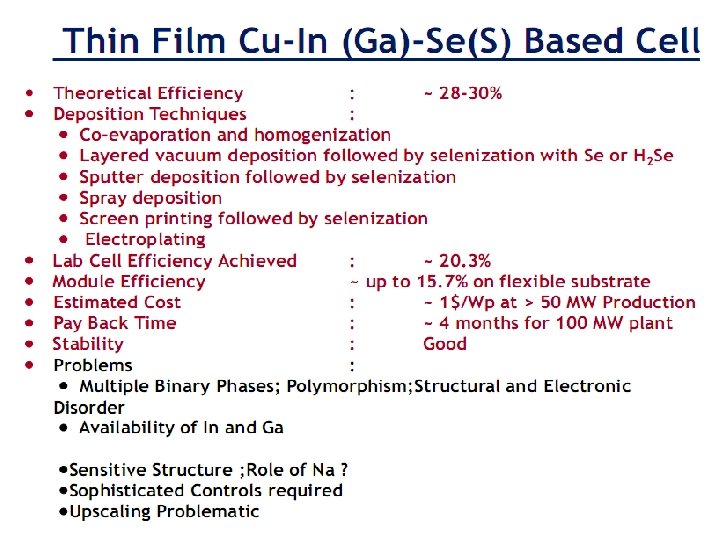
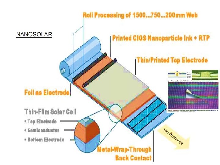
Solar Cell Technologies • Crystalline Silicon solar cells - Single, Multi, Ribbon • Thin Film solar cells - Silicon, Cu 2 S , a-Si, m-Si, n-Si, Cd. Te, CIGS, CNTS • Concentrating solar cells - Si, Ga. As • Dye, Organic , Hybrid & other emerging solar cells • New Ideas 44
Crystalline Silicon : Present Scenario o Efficiency of single crystal Si cells (Laboratory) has been rising steadily to ~ 25% as a result of better understanding of the junction properties and innovations in cell design and fabrication technologies. o The world PV production of ~ 7900 MW in FY 2009 is primarily (~ 93%) based on single, crystal and polycrystalline silicon. o With increasing production of Si-PV from 200 k. W in 1976 to 6900 MW in 2008, the cost of solar cells has decreased from $100 to about $3/Wp. o With the existing technology and the material cost, the cost of Si cells can not be 45
Crystalline Silicon : Present Scenario o Present day technology uses 8”or larger pseudo square of ~ 200μ m thickness, with an efficiency of ~ 15 -16%. The energy (16 -5 k. WH/Wp) pay back period of such cells is ~3 -4 years. The module life is about 25 years. o Specially designed silicon solar cells with efficiency ~ 18 -20% are being manufactured on a limited scale for special applications (e. g for concentration). o Polycrystalline silicon solar cells with efficiency ~ 12 -14% are being produced on large scale. o Specially designed thin(~ 20 m) films silicon solar cells with efficiency ~ 12% have been fabricated on a lab scale. Production of hybrid thin film Si cells on MW scale is being pursued 46
Single, Tandem & Triple Junction Si Solar Cells
Triple Junction a-Si: H/Si. Ge: H/nc-Si: H Solar Cells Initial efficiency: 15. 1%; Stable efficiency: 13. 3%
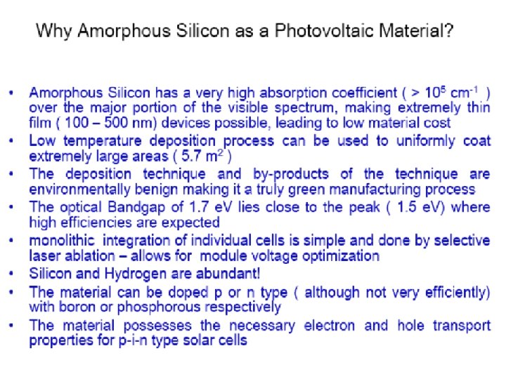
Amorphous Silicon (a-Si-H) : A Review
Gretzel- Dye Sensitive Solar Cell
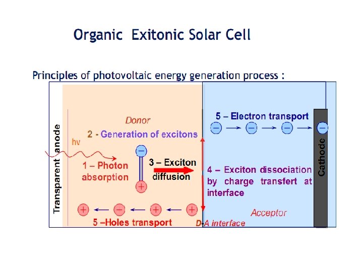
Organic Solar Cell
History of Organic Solar Cell
Summary of Exitonic-Organic Solar Cell
Efficiency Enhancement by Fundamental Processes
Thank You Q&A