Registers and Counters 1 What is a Register
- Slides: 46

Registers and Counters 1

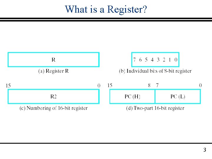
What is a Register? · A Register is a collection of n flip-flops with some common function or characteristic § Control signals - common clock, clear, load, etc. § Function - part of multi-bit storage, counter, or shift register · At a minimum, we must be able to: § Observe the stored binary value § Change the stored binary value 2

What is a Register? 3

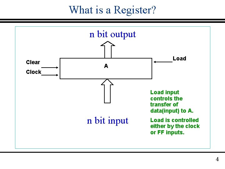
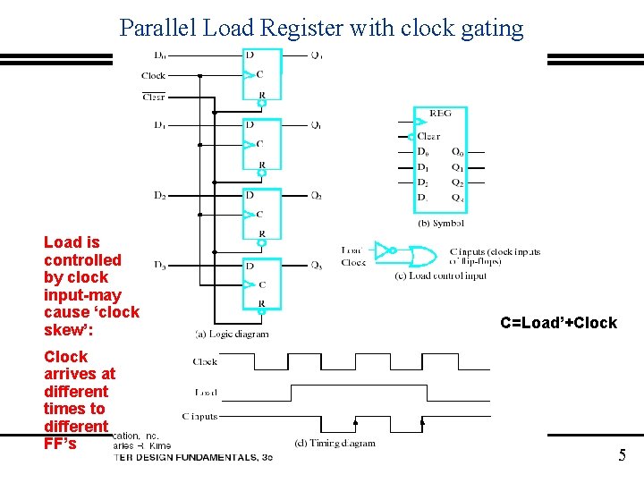
What is a Register? n bit output Clear Clock Load A Load input controls the transfer of data(input) to A. n bit input Load is controlled either by the clock or FF inputs. 4

Parallel Load Register with clock gating Load is controlled by clock input-may cause ‘clock skew’: Clock arrives at different times to different FF’s C=Load’+Clock 5

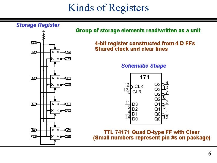
Kinds of Registers Storage Register Group of storage elements read/written as a unit V+ CLR D 3 D Q Q 3 C Q Q 3 F 4 -bit register constructed from 4 D FFs Shared clock and clear lines Schematic Shape D 2 D 1 D Q Q 2 C Q Q 2 F D Q Q 1 C Q Q 1 F D 0 D Q Q 0 CLK C Q Q 0 F TTL 74171 Quad D-type FF with Clear (Small numbers represent pin #s on package) 6

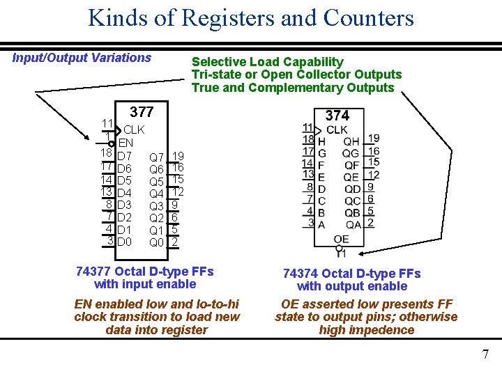
Kinds of Registers and Counters Input/Output Variations 11 1 18 17 14 13 8 7 4 3 Selective Load Capability Tri-state or Open Collector Outputs True and Complementary Outputs 377 CLK EN D 7 D 6 D 5 D 4 D 3 D 2 D 1 D 0 Q 7 Q 6 Q 5 Q 4 Q 3 Q 2 Q 1 Q 0 19 16 15 12 9 6 5 2 74377 Octal D-type FFs with input enable EN enabled low and lo-to-hi clock transition to load new data into register 74374 Octal D-type FFs with output enable OE asserted low presents FF state to output pins; otherwise high impedence 7

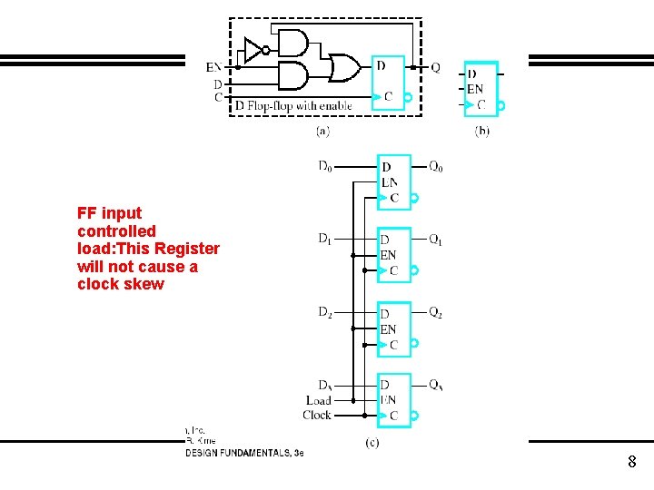
FF input controlled load: This Register will not cause a clock skew 8

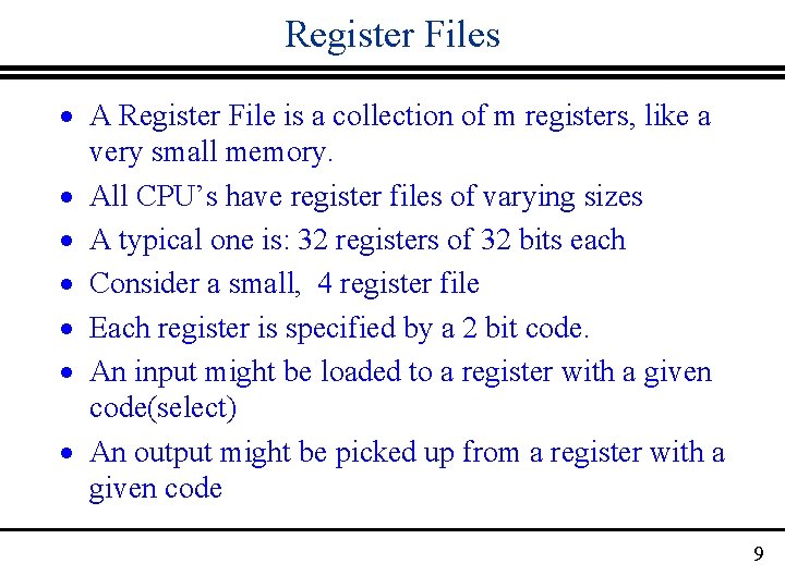
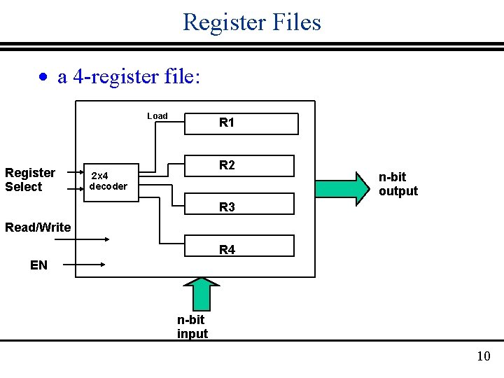
Register Files · A Register File is a collection of m registers, like a very small memory. · All CPU’s have register files of varying sizes · A typical one is: 32 registers of 32 bits each · Consider a small, 4 register file · Each register is specified by a 2 bit code. · An input might be loaded to a register with a given code(select) · An output might be picked up from a register with a given code 9

Register Files · a 4 -register file: Load Register Select R 1 R 2 2 x 4 decoder n-bit output R 3 Read/Write R 4 EN n-bit input 10

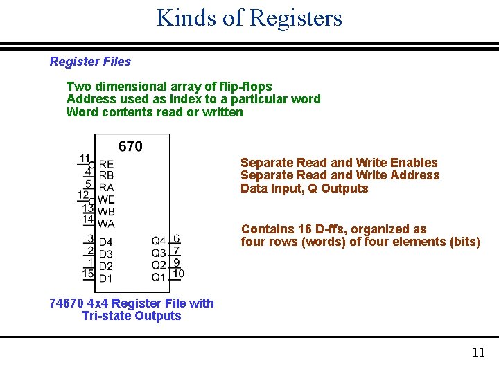
Kinds of Registers Register Files Two dimensional array of flip-flops Address used as index to a particular word Word contents read or written Separate Read and Write Enables Separate Read and Write Address Data Input, Q Outputs Contains 16 D-ffs, organized as four rows (words) of four elements (bits) 74670 4 x 4 Register File with Tri-state Outputs 11

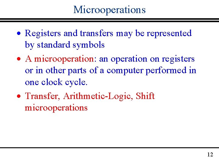
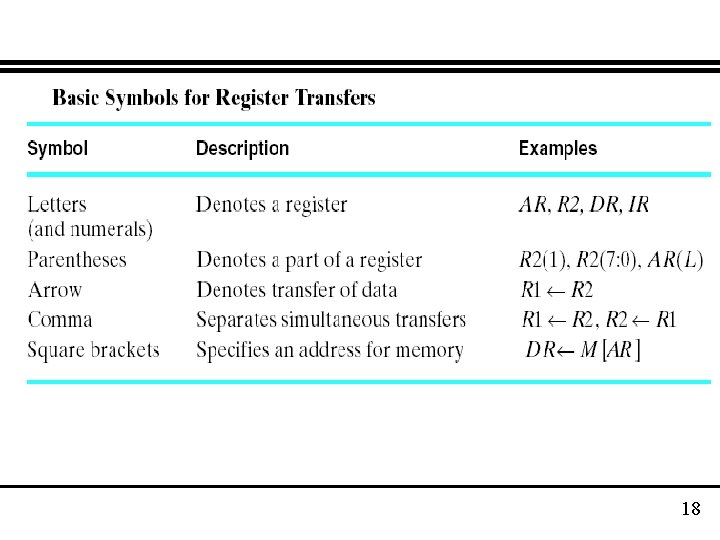
Microoperations · Registers and transfers may be represented by standard symbols · A microoperation: an operation on registers or in other parts of a computer performed in one clock cycle. · Transfer, Arithmetic-Logic, Shift microoperations 12

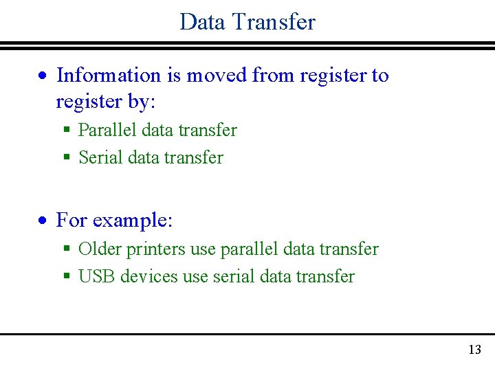
Data Transfer · Information is moved from register to register by: § Parallel data transfer § Serial data transfer · For example: § Older printers use parallel data transfer § USB devices use serial data transfer 13

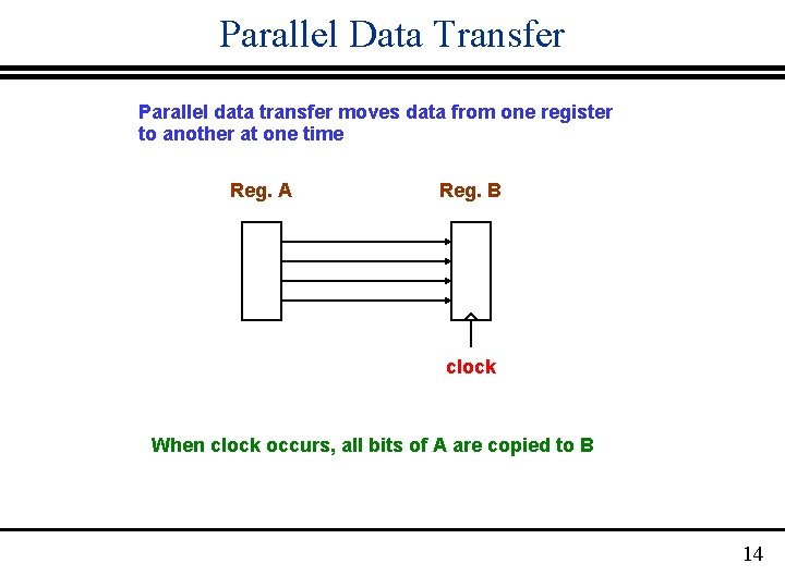
Parallel Data Transfer Parallel data transfer moves data from one register to another at one time Reg. A Reg. B clock When clock occurs, all bits of A are copied to B 14

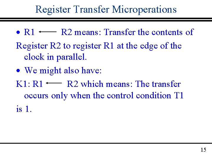
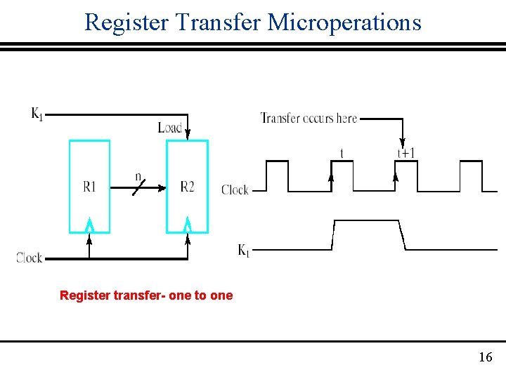
Register Transfer Microperations · R 1 R 2 means: Transfer the contents of Register R 2 to register R 1 at the edge of the clock in parallel. · We might also have: K 1: R 1 R 2 which means: The transfer occurs only when the control condition T 1 is 1. 15

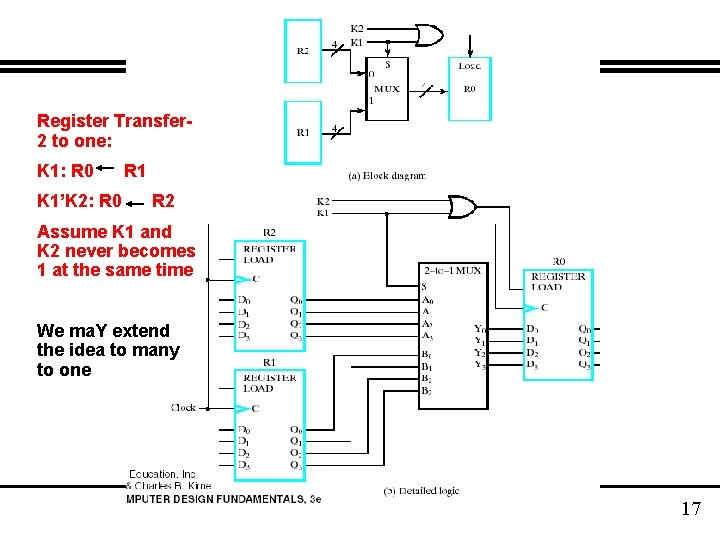
Register Transfer Microperations Register transfer- one to one 16

Register Transfer 2 to one: K 1: R 0 K 1’K 2: R 0 R 1 R 2 Assume K 1 and K 2 never becomes 1 at the same time We ma. Y extend the idea to many to one 17

18

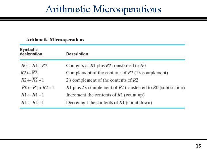
Arithmetic Microoperations 19

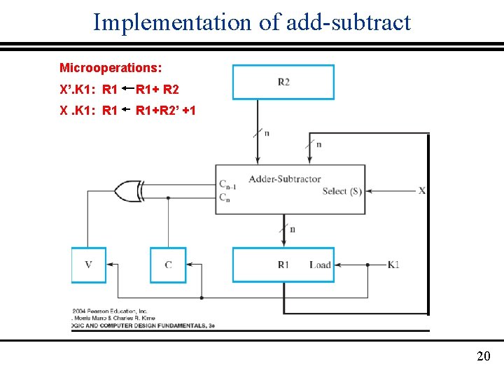
Implementation of add-subtract Microoperations: X’. K 1: R 1+ R 2 X. K 1: R 1+R 2’ +1 20

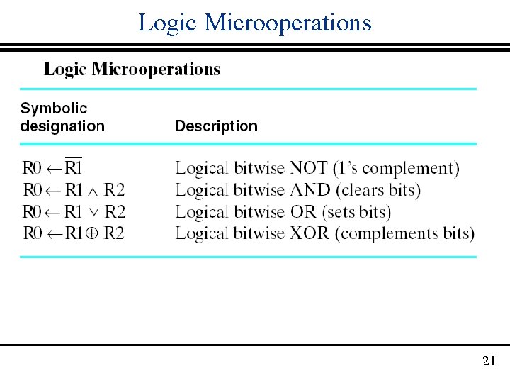
Logic Microoperations 21

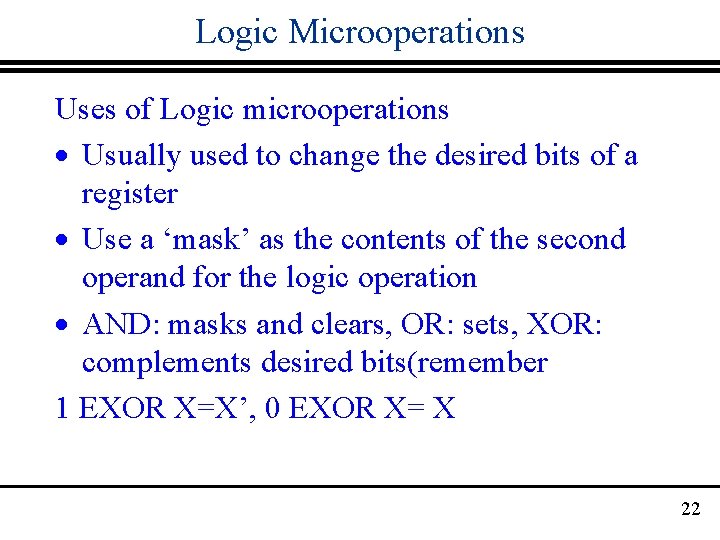
Logic Microoperations Uses of Logic microoperations · Usually used to change the desired bits of a register · Use a ‘mask’ as the contents of the second operand for the logic operation · AND: masks and clears, OR: sets, XOR: complements desired bits(remember 1 EXOR X=X’, 0 EXOR X= X 22

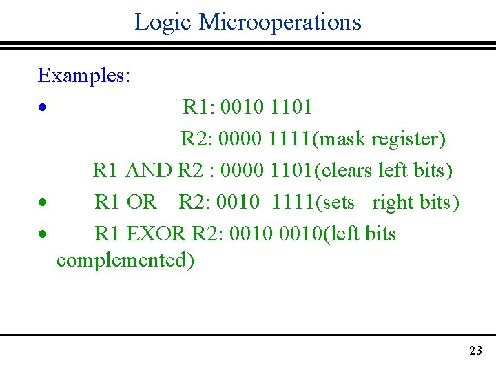
Logic Microoperations Examples: · R 1: 0010 1101 R 2: 0000 1111(mask register) R 1 AND R 2 : 0000 1101(clears left bits) · R 1 OR R 2: 0010 1111(sets right bits) · R 1 EXOR R 2: 0010(left bits complemented) 23

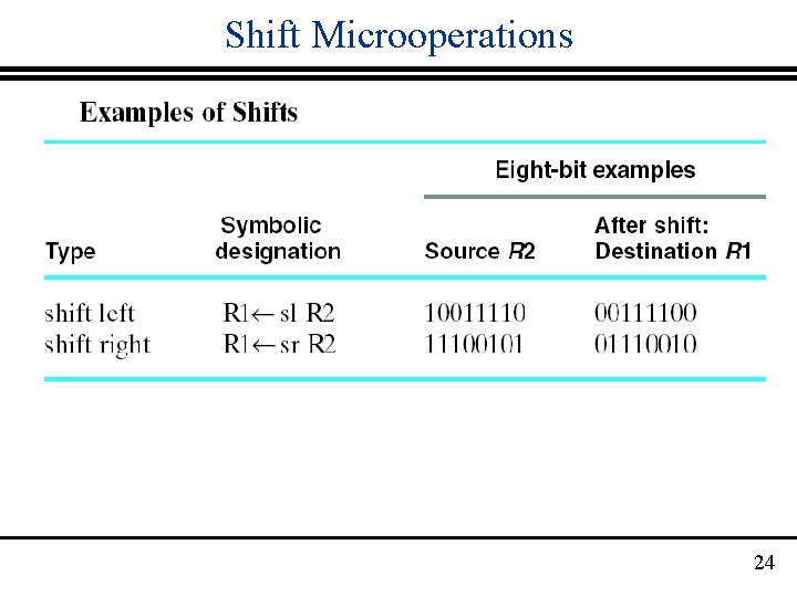
Shift Microoperations 24

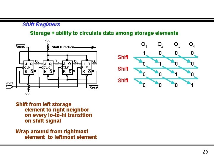
Shift Registers Storage + ability to circulate data among storage elements Vcc Reset Shift Direction J Q Q 1 J Q Q 2 J Q Q 3 J Q CLK CLK K Q K Q Q 4 Shift Reset Q 1 Q 2 Q 3 Q 4 1 0 0 0 0 1 Vcc Shift from left storage element to right neighbor on every lo-to-hi transition on shift signal Wrap around from rightmost element to leftmost element 25

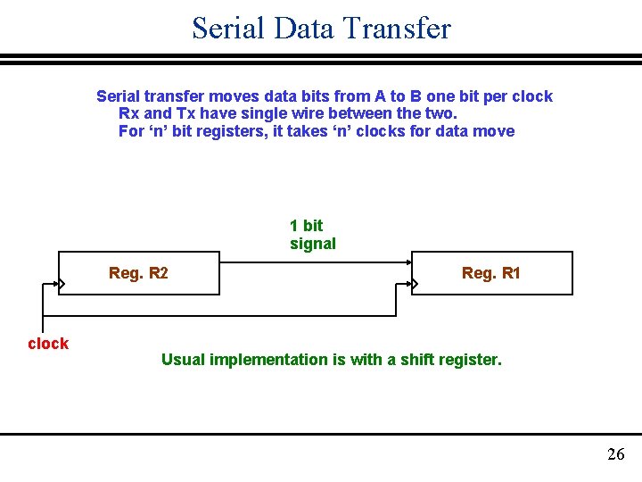
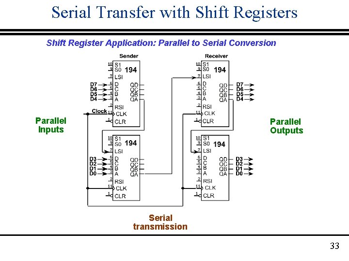
Serial Data Transfer Serial transfer moves data bits from A to B one bit per clock Rx and Tx have single wire between the two. For ‘n’ bit registers, it takes ‘n’ clocks for data move 1 bit signal Reg. R 2 clock Reg. R 1 Usual implementation is with a shift register. 26

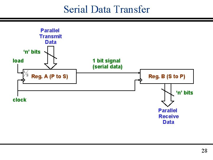
Serial Data Transfer · Typical serial transfer is a multi-step process § Load transmit shift register with data to send § Shift data bit by bit from transmit to receive SR § Transfer received data to other registers · The transmit SR must have parallel load § AKA parallel to serial shift register · The receive SR must have parallel outputs § AKA serial to parallel shift register · Other control/timing signals usually needed 27

Serial Data Transfer Parallel Transmit Data ‘n’ bits load 1 bit signal (serial data) Reg. A (P to S) Reg. B (S to P) ‘n’ bits clock Parallel Receive Data 28

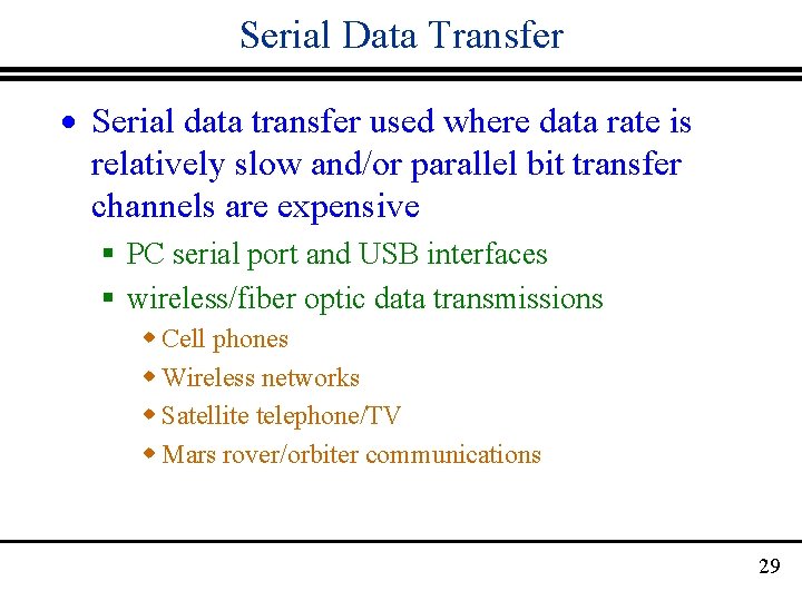
Serial Data Transfer · Serial data transfer used where data rate is relatively slow and/or parallel bit transfer channels are expensive § PC serial port and USB interfaces § wireless/fiber optic data transmissions w Cell phones w Wireless networks w Satellite telephone/TV w Mars rover/orbiter communications 29

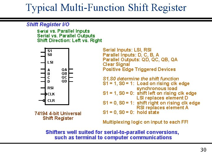
Typical Multi-Function Shift Register I/O Serial vs. Parallel Inputs Serial vs. Parallel Outputs Shift Direction: Left vs. Right S 1 S 0 LSI A B C D QA QB QC QD RSI CLK CLR 74194 4 -bit Universal Shift Register Serial Inputs: LSI, RSI Parallel Inputs: D, C, B, A Parallel Outputs: QD, QC, QB, QA Clear Signal Positive Edge Triggered Devices S 1, S 0 determine the shift function S 1 = 1, S 0 = 1: Load on rising clk edge synchronous load S 1 = 1, S 0 = 0: shift left on rising clk edge LSI replaces element D S 1 = 0, S 0 = 1: shift right on rising clk edge RSI replaces element A S 1 = 0, S 0 = 0: hold state Multiplexing logic on input to each FF! Shifters well suited for serial-to-parallel conversions, such as terminal to computer communications 30

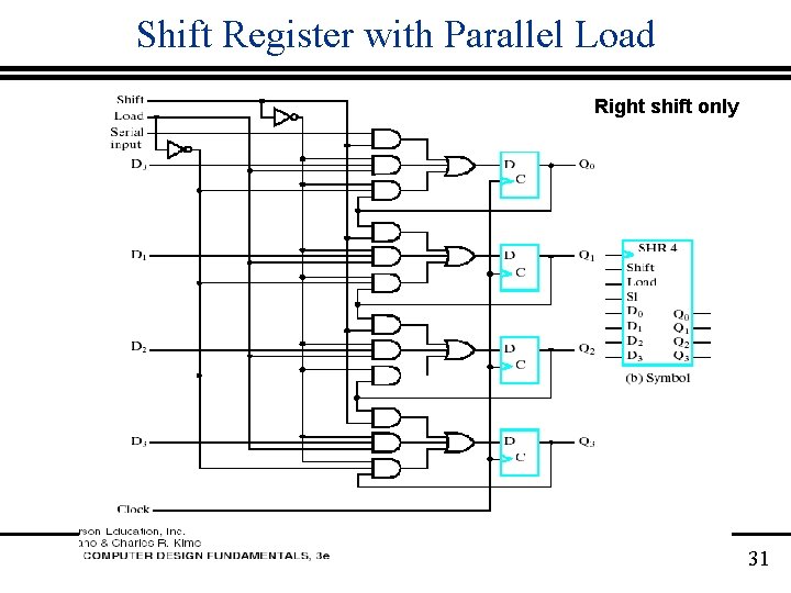
Shift Register with Parallel Load Right shift only 31

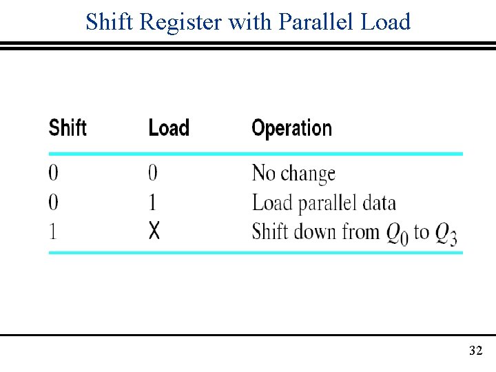
Shift Register with Parallel Load 32

Serial Transfer with Shift Registers Shift Register Application: Parallel to Serial Conversion Parallel Inputs Parallel Outputs Serial transmission 33

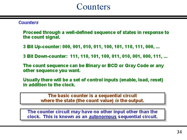
Counters Proceed through a well-defined sequence of states in response to the count signal. 3 Bit Up-counter: 000, 001, 010, 011, 100, 101, 110, 111, 000, . . . 3 Bit Down-counter: 111, 110, 101, 100, 011, 010, 001, 000, 111, . . . The count sequence can be Binary or BCD or Gray Code or any other sequence you want. Usually there will be a set of control inputs (enable, load, reset) in addition to the clock. The basic counter is a sequential circuit where the state (the count value) is the output. The counter circuit may have no other input other than the clock. This is known as an autonomous sequential circuit. 34

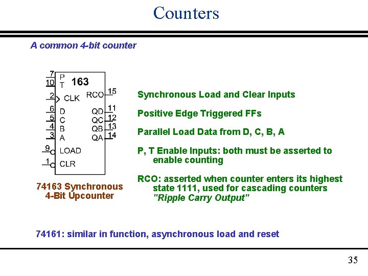
Counters A common 4 -bit counter Synchronous Load and Clear Inputs Positive Edge Triggered FFs Parallel Load Data from D, C, B, A P, T Enable Inputs: both must be asserted to enable counting 74163 Synchronous 4 -Bit Upcounter RCO: asserted when counter enters its highest state 1111, used for cascading counters "Ripple Carry Output" 74161: similar in function, asynchronous load and reset 35

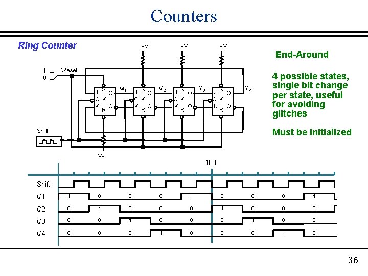
Counters Ring Counter 1 0 +V +V +V End-Around Reset S J Q CLK K Q R Q 1 S J Q CLK K Q R Q 2 S J Q CLK K Q R Q 3 S J Q CLK K Q R Q 4 4 possible states, single bit change per state, useful for avoiding glitches Must be initialized Shift V+ 100 Shift Q 1 1 0 0 0 1 Q 2 0 1 0 0 0 Q 3 0 0 1 0 0 Q 4 0 0 0 1 0 36

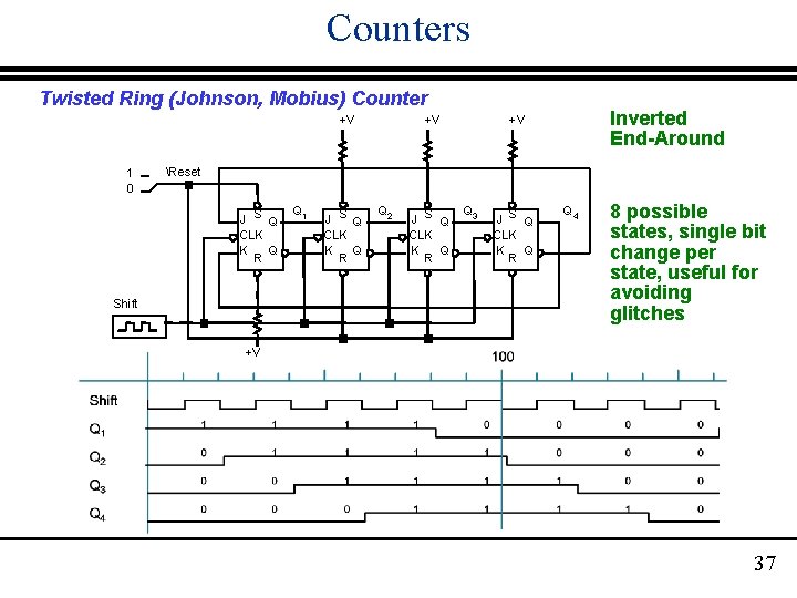
Counters Twisted Ring (Johnson, Mobius) Counter +V 1 0 +V Inverted End-Around +V Reset S J Q CLK K Q R Shift Q 1 S J Q CLK K Q R Q 2 S J Q CLK K Q R Q 3 S J Q CLK K Q R Q 4 8 possible states, single bit change per state, useful for avoiding glitches +V 37

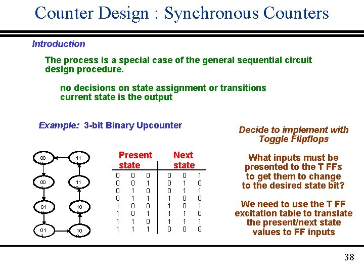
Counter Design : Synchronous Counters Introduction The process is a special case of the general sequential circuit design procedure. no decisions on state assignment or transitions current state is the output Example: 3 -bit Binary Upcounter 00 0 11 1 00 1 11 0 01 0 10 1 01 1 10 0 Present state 0 0 1 1 0 1 0 1 Decide to implement with Toggle Flipflops Next state 0 0 0 1 1 0 1 0 1 0 What inputs must be presented to the T FFs to get them to change to the desired state bit? We need to use the T FF excitation table to translate the present/next state values to FF inputs 38

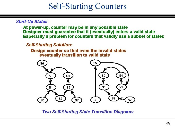
Self-Starting Counters Start-Up States At power-up, counter may be in any possible state Designer must guarantee that it (eventually) enters a valid state Especially a problem for counters that validly use a subset of states Self-Starting Solution: Design counter so that even the invalid states eventually transition to valid state S 5 S 6 S 5 S 0 S 4 S 1 S 3 S 2 S 7 S 6 S 2 S 7 Two Self-Starting State Transition Diagrams 39

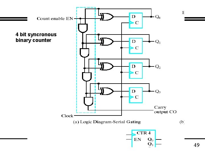
4 bit syncronous binary counter 49

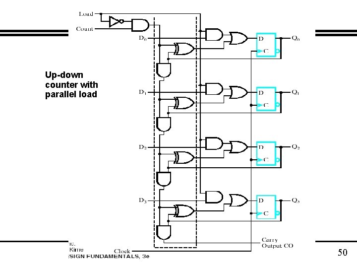
Up-down counter with parallel load 50

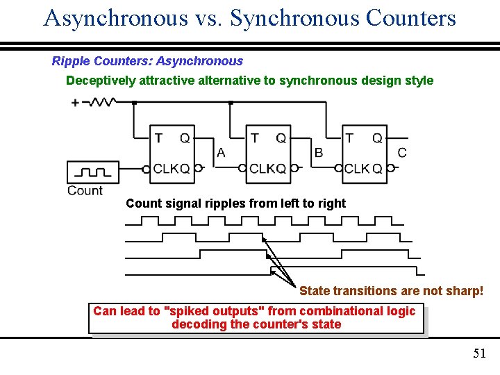
Asynchronous vs. Synchronous Counters Ripple Counters: Asynchronous Deceptively attractive alternative to synchronous design style Count signal ripples from left to right State transitions are not sharp! Can lead to "spiked outputs" from combinational logic decoding the counter's state 51

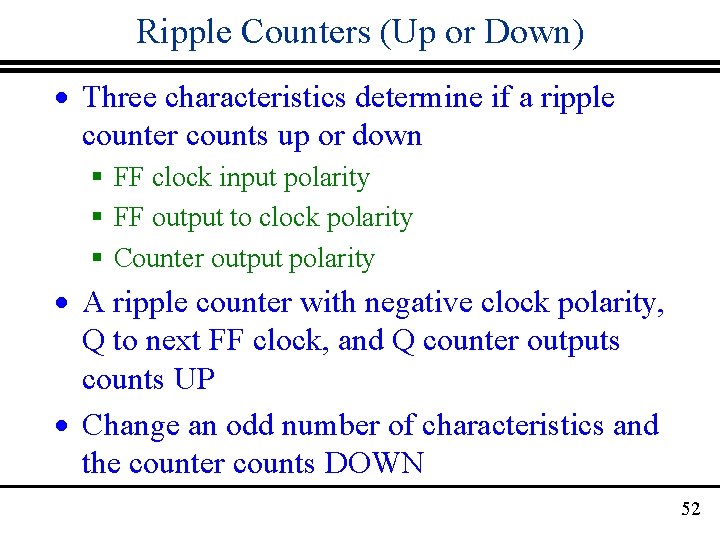
Ripple Counters (Up or Down) · Three characteristics determine if a ripple counter counts up or down § FF clock input polarity § FF output to clock polarity § Counter output polarity · A ripple counter with negative clock polarity, Q to next FF clock, and Q counter outputs counts UP · Change an odd number of characteristics and the counter counts DOWN 52

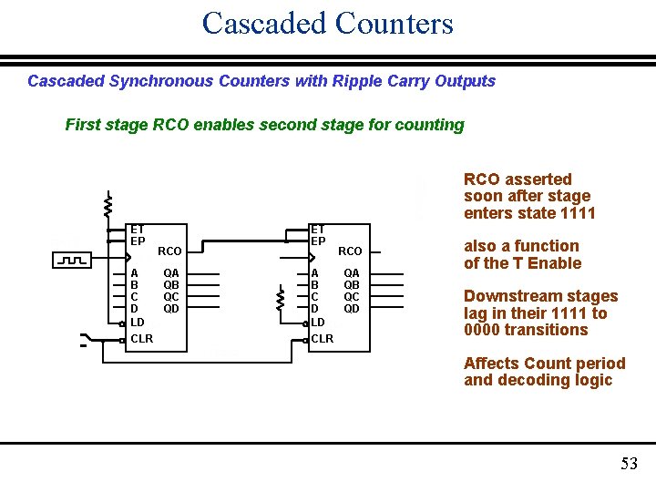
Cascaded Counters Cascaded Synchronous Counters with Ripple Carry Outputs First stage RCO enables second stage for counting RCO asserted soon after stage enters state 1111 ET EP A B C D LD CLR RCO QA QB QC QD also a function of the T Enable Downstream stages lag in their 1111 to 0000 transitions Affects Count period and decoding logic 53

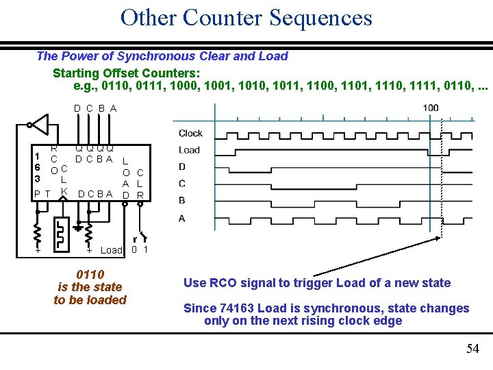
Other Counter Sequences The Power of Synchronous Clear and Load Starting Offset Counters: e. g. , 0110, 0111, 1000, 1001, 1010, 1011, 1100, 1101, 1110, 1111, 0110, . . . D C B A R Q Q QQ C D CBA C O L P T K DCBA 1 6 3 + L O C A L D R + Load 0 1 0110 is the state to be loaded Use RCO signal to trigger Load of a new state Since 74163 Load is synchronous, state changes only on the next rising clock edge 54

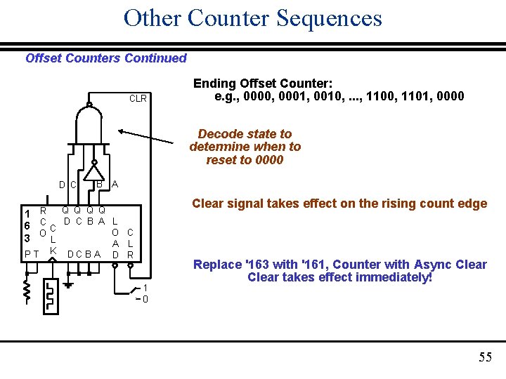
Other Counter Sequences Offset Counters Continued CLR Ending Offset Counter: e. g. , 0000, 0001, 0010, . . . , 1100, 1101, 0000 Decode state to determine when to reset to 0000 D C 1 6 3 P B Q Q R D C B A C C O L T K DCBA A Clear signal takes effect on the rising count edge L O C A L D R 1 0 Replace '163 with '161, Counter with Async Clear takes effect immediately! 55