Memory Hierarchy Nizamettin AYDIN naydinyildiz edu tr http

- Slides: 97

Memory Hierarchy Nizamettin AYDIN naydin@yildiz. edu. tr http: //www. yildiz. edu. tr/~naydin

Introduction • Memory lies at the heart of the storedprogram computer. • In this lecture, we focus on memory organization. A clear understanding of these ideas is essential for the analysis of system performance.

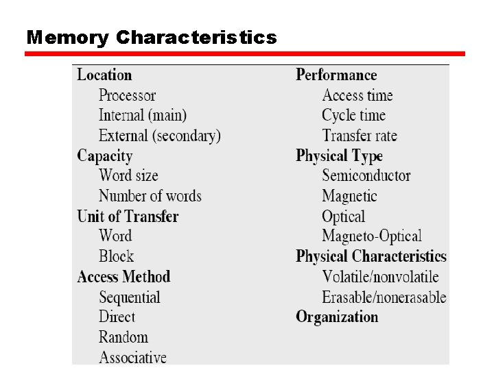
Memory Characteristics

Unit of Transfer • Internal —Usually governed by data bus width • External —Usually a block which is much larger than a word • Addressable unit —Smallest location which can be uniquely addressed —Word internally —Cluster on M$ disks

Access Methods (1) • Sequential —Start at the beginning and read through in order —Access time depends on location of data and previous location —e. g. tape • Direct —Individual blocks have unique address —Access is by jumping to vicinity plus sequential search —Access time depends on location and previous location —e. g. disk

Access Methods (2) • Random —Individual addresses identify locations exactly —Access time is independent of location or previous access —e. g. RAM • Associative —Data is located by a comparison with contents of a portion of the store —Access time is independent of location or previous access —e. g. cache

Performance • Access time —Time between presenting the address and getting the valid data • Memory Cycle time —Time may be required for the memory to “recover” before next access —Cycle time is access + recovery • Transfer Rate —Rate at which data can be moved

Physical Types • Semiconductor —RAM • Magnetic —Disk & Tape • Optical —CD & DVD • Others —Bubble —Hologram

Physical Characteristics • • Decay Volatility Erasable Power consumption

Organisation • Physical arrangement of bits into words • Not always obvious • e. g. interleaved

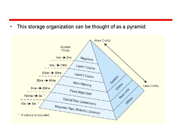
The Memory Hierarchy • Generally speaking, faster memory is more expensive than slower memory. • To provide the best performance at the lowest cost, memory is organized in a hierarchical fashion. • Small, fast storage elements are kept in the CPU, larger, slower main memory is accessed through the data bus. • Larger, (almost) permanent storage in the form of disk and tape drives is still further from the CPU.

Memory Hierarchy • Registers —In CPU • Internal or Main memory —May include one or more levels of cache —“RAM” • External memory —Backing store

The Memory Hierarchy • This storage organization can be thought of as a pyramid:

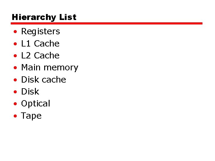
Hierarchy List • • Registers L 1 Cache L 2 Cache Main memory Disk cache Disk Optical Tape

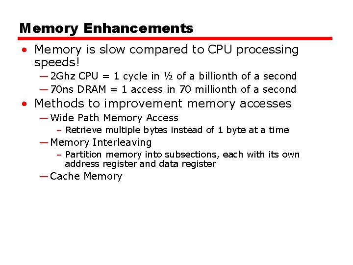
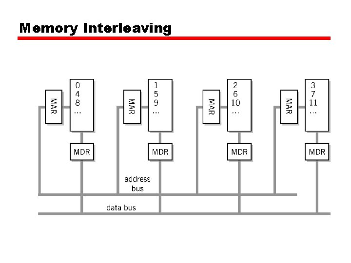
Memory Enhancements • Memory is slow compared to CPU processing speeds! — 2 Ghz CPU = 1 cycle in ½ of a billionth of a second — 70 ns DRAM = 1 access in 70 millionth of a second • Methods to improvement memory accesses — Wide Path Memory Access – Retrieve multiple bytes instead of 1 byte at a time — Memory Interleaving – Partition memory into subsections, each with its own address register and data register — Cache Memory

Memory Interleaving

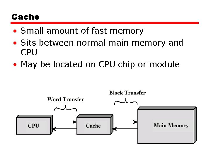
Cache • Small amount of fast memory • Sits between normal main memory and CPU • May be located on CPU chip or module

Why Cache? • Even the fastest hard disk has an access time of about 10 milliseconds • 2 Ghz CPU waiting 10 milliseconds wastes 20 million clock cycles!

Cache Memory • Blocks: 8 or 16 bytes • Tags: location in main memory • Cache controller — hardware that checks tags • Cache Line — Unit of transfer between storage and cache memory • Hit Ratio: ratio of hits out of total requests • Synchronizing cache and memory — Write through — Write back

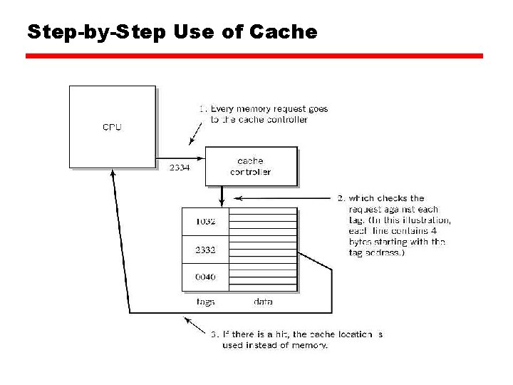
Step-by-Step Use of Cache

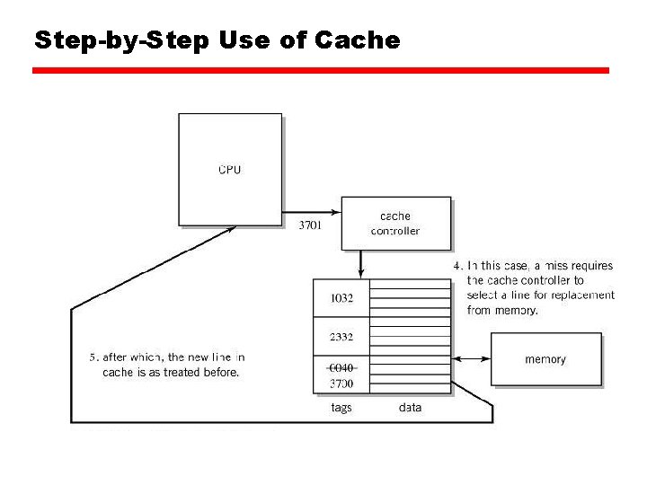
Step-by-Step Use of Cache

Cache vs. Virtual Memory • Cache speeds up memory access • Virtual memory increases amount of perceived storage —independence from the configuration and capacity of the memory system —low cost per bit

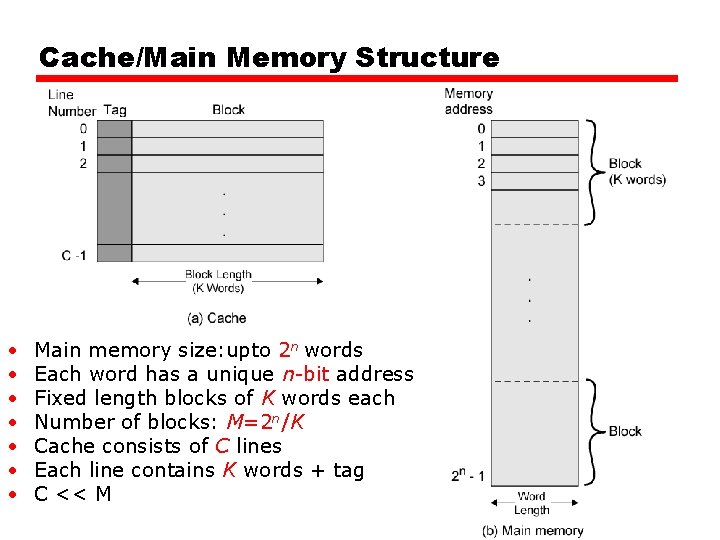
Cache/Main Memory Structure • • Main memory size: upto 2 n words Each word has a unique n-bit address Fixed length blocks of K words each Number of blocks: M=2 n/K Cache consists of C lines Each line contains K words + tag C << M

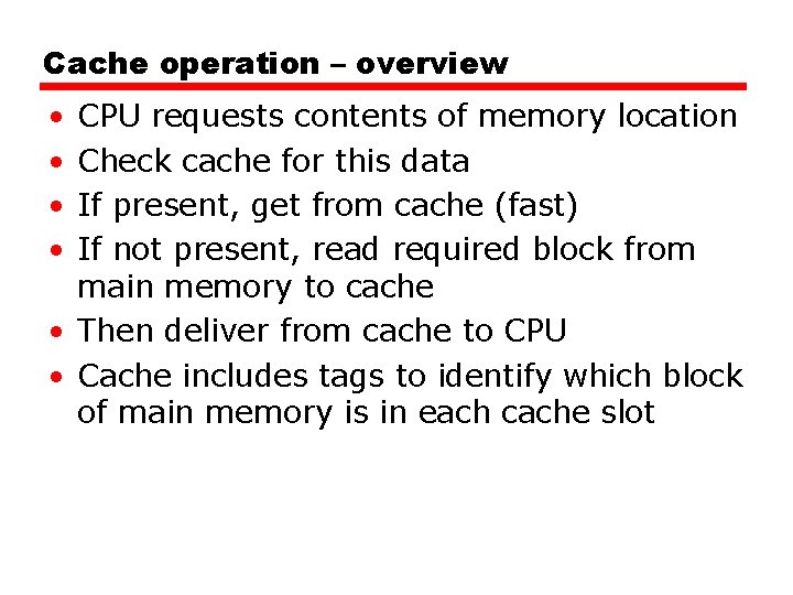
Cache operation – overview • • CPU requests contents of memory location Check cache for this data If present, get from cache (fast) If not present, read required block from main memory to cache • Then deliver from cache to CPU • Cache includes tags to identify which block of main memory is in each cache slot

Cache Design • • • Size Mapping Function Replacement Algorithm Write Policy Block Size Number of Caches

Size does matter • Cost —More cache is expensive • Speed —More cache is faster (up to a point) —Checking cache for data takes time

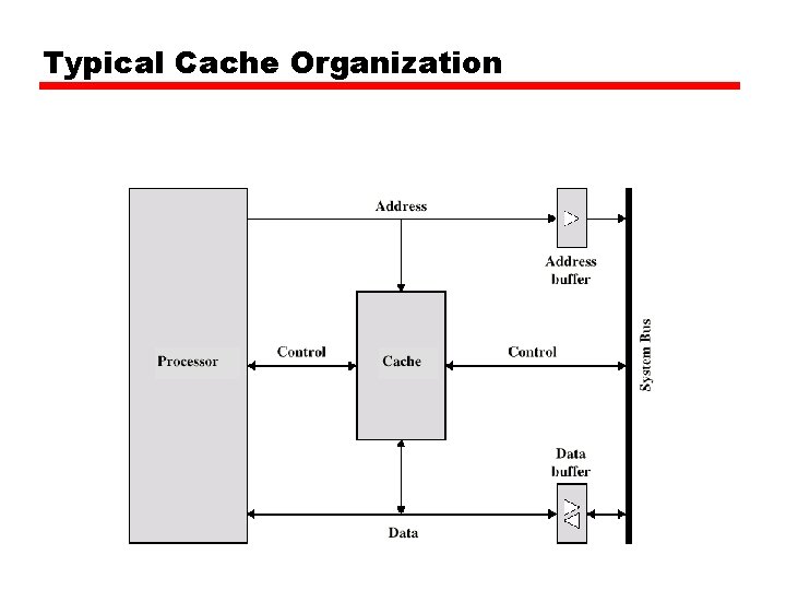
Typical Cache Organization

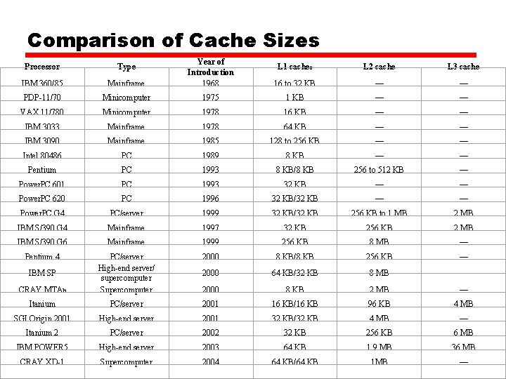
Comparison of Cache Sizes L 1 cachea L 2 cache L 3 cache Mainframe Year of Introduction 1968 16 to 32 KB — — PDP-11/70 Minicomputer 1975 1 KB — — VAX 11/780 Minicomputer 1978 16 KB — — IBM 3033 Mainframe 1978 64 KB — — IBM 3090 Mainframe 1985 128 to 256 KB — — Intel 80486 PC 1989 8 KB — — Pentium PC 1993 8 KB/8 KB 256 to 512 KB — Power. PC 601 PC 1993 32 KB — — Power. PC 620 PC 1996 32 KB/32 KB — — Power. PC G 4 PC/server 1999 32 KB/32 KB 256 KB to 1 MB 2 MB IBM S/390 G 4 Mainframe 1997 32 KB 256 KB 2 MB IBM S/390 G 6 Mainframe 1999 256 KB 8 MB — Pentium 4 2000 8 KB/8 KB 256 KB — 2000 64 KB/32 KB 8 MB — CRAY MTAb PC/server High-end server/ supercomputer Supercomputer 2000 8 KB 2 MB — Itanium PC/server 2001 16 KB/16 KB 96 KB 4 MB SGI Origin 2001 High-end server 2001 32 KB/32 KB 4 MB — Itanium 2 PC/server 2002 32 KB 256 KB 6 MB IBM POWER 5 High-end server 2003 64 KB 1. 9 MB 36 MB CRAY XD-1 Supercomputer 2004 64 KB/64 KB 1 MB — Processor Type IBM 360/85 IBM SP

Mapping Function • Because there are fewer lines than main memory blocks, an algorithm is needed for mapping main memory blocks into cache lines. • Which main memory block currently occupies a cache line? • Three techniques can be used: —Direct mapping —Associative mapping —Set associative mapping

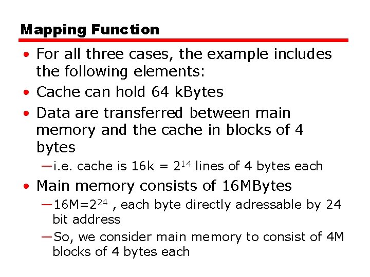
Mapping Function • For all three cases, the example includes the following elements: • Cache can hold 64 k. Bytes • Data are transferred between main memory and the cache in blocks of 4 bytes —i. e. cache is 16 k = 214 lines of 4 bytes each • Main memory consists of 16 MBytes — 16 M=224 , each byte directly adressable by 24 bit address —So, we consider main memory to consist of 4 M blocks of 4 bytes each

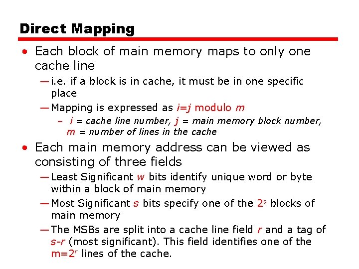
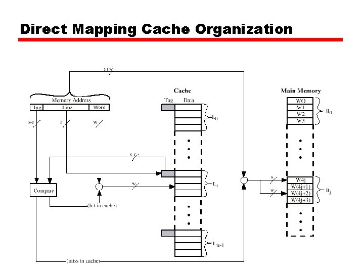
Direct Mapping • Each block of main memory maps to only one cache line — i. e. if a block is in cache, it must be in one specific place — Mapping is expressed as i=j modulo m – i = cache line number, j = main memory block number, m = number of lines in the cache • Each main memory address can be viewed as consisting of three fields — Least Significant w bits identify unique word or byte within a block of main memory — Most Significant s bits specify one of the 2 s blocks of main memory — The MSBs are split into a cache line field r and a tag of s-r (most significant). This field identifies one of the m=2 r lines of the cache.

Direct Mapping Cache Organization

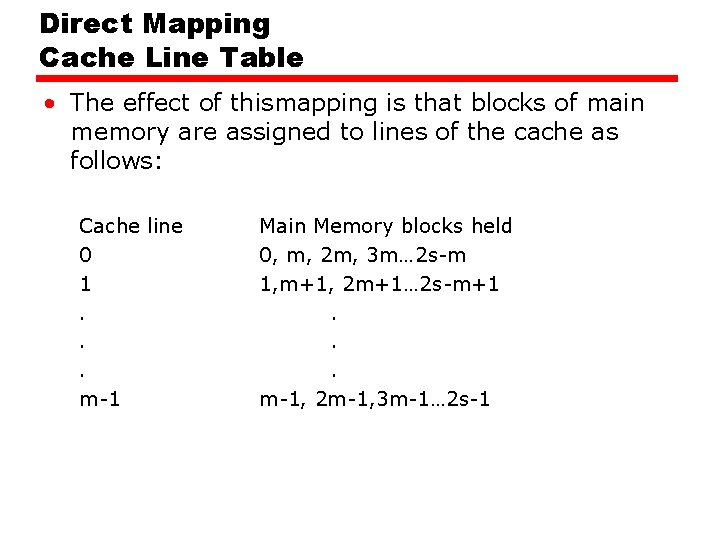
Direct Mapping Cache Line Table • The effect of thismapping is that blocks of main memory are assigned to lines of the cache as follows: Cache line 0 1. . . m-1 Main Memory blocks held 0, m, 2 m, 3 m… 2 s-m 1, m+1, 2 m+1… 2 s-m+1. . . m-1, 2 m-1, 3 m-1… 2 s-1

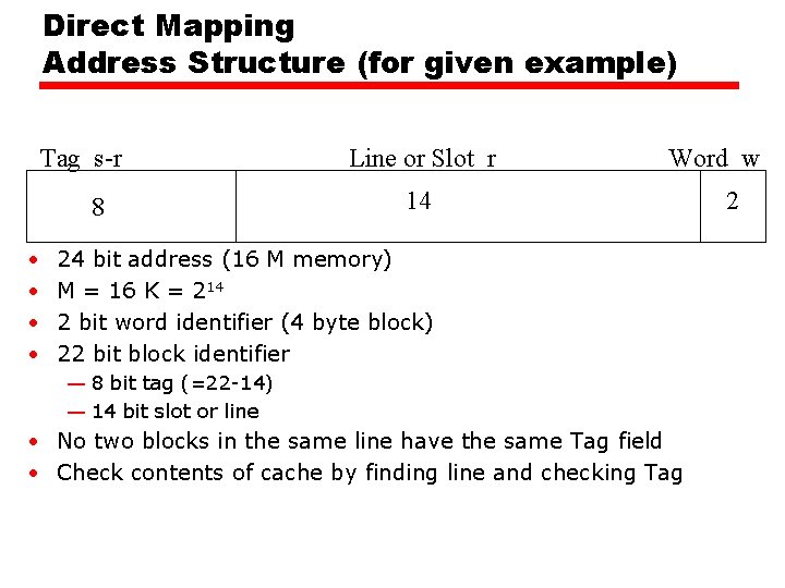
Direct Mapping Address Structure (for given example) Tag s-r 8 • • Line or Slot r Word w 14 24 bit address (16 M memory) M = 16 K = 214 2 bit word identifier (4 byte block) 22 bit block identifier — 8 bit tag (=22 -14) — 14 bit slot or line • No two blocks in the same line have the same Tag field • Check contents of cache by finding line and checking Tag 2

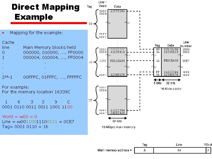
Direct Mapping Example • Mapping for the example: Cache line 0 1. . . 214 -1 Main Memory blocks held 000000, 010000, . . . , FF 000004, 010004, . . . , FF 0004. . . 00 FFFC, 01 FFFC, . . . , FFFFFC For example: For the memory location 16339 C 1 6 3 3 9 C 0001 0110 0011 1001 1100 Word = 0000 = 0 Line = 000011100111 = 0 CE 7 Tag= 0001 0110 = 16

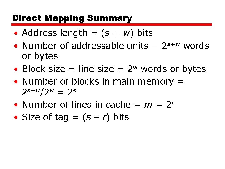
Direct Mapping Summary • Address length = (s + w) bits • Number of addressable units = 2 s+w words or bytes • Block size = line size = 2 w words or bytes • Number of blocks in main memory = 2 s+w/2 w = 2 s • Number of lines in cache = m = 2 r • Size of tag = (s – r) bits

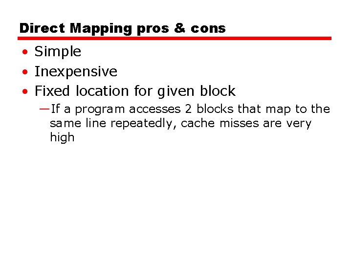
Direct Mapping pros & cons • Simple • Inexpensive • Fixed location for given block —If a program accesses 2 blocks that map to the same line repeatedly, cache misses are very high

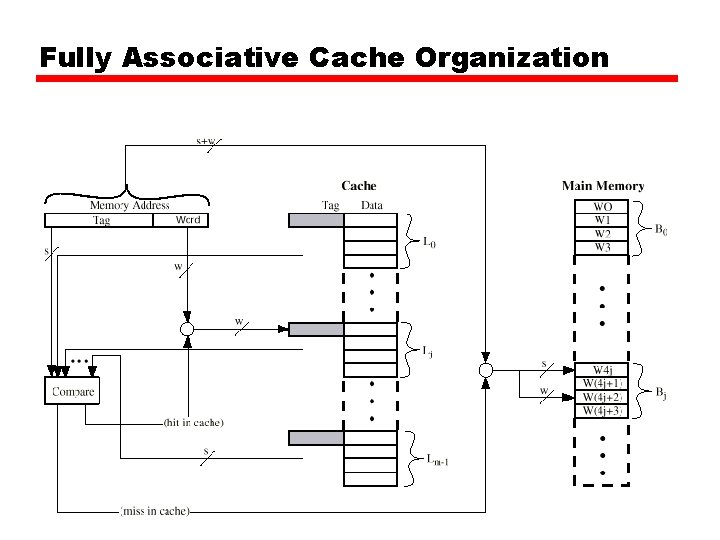
Associative Mapping • A main memory block can load into any line of cache • Memory address is interpreted as tag and word • Tag uniquely identifies block of memory • Every line’s tag is examined for a match • Cache searching gets expensive

Fully Associative Cache Organization

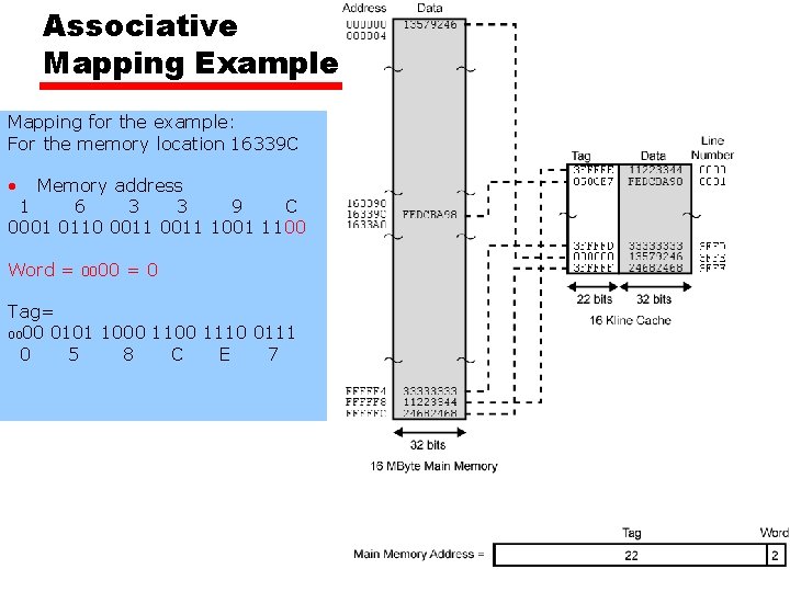
Associative Mapping Example Mapping for the example: For the memory location 16339 C • Memory address 1 6 3 3 9 C 0001 0110 0011 1001 1100 Word = 0000 =0 Tag= 0000 0101 1000 1110 0111 0 5 8 C E 7

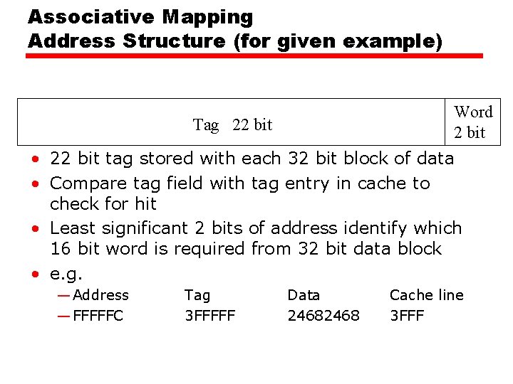
Associative Mapping Address Structure (for given example) Word 2 bit Tag 22 bit • 22 bit tag stored with each 32 bit block of data • Compare tag field with tag entry in cache to check for hit • Least significant 2 bits of address identify which 16 bit word is required from 32 bit data block • e. g. — Address — FFFFFC Tag 3 FFFFF Data 2468 Cache line 3 FFF

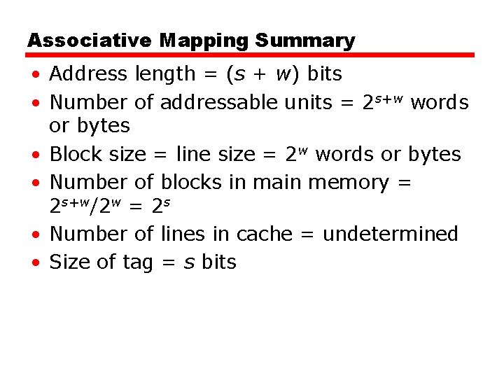
Associative Mapping Summary • Address length = (s + w) bits • Number of addressable units = 2 s+w words or bytes • Block size = line size = 2 w words or bytes • Number of blocks in main memory = 2 s+w/2 w = 2 s • Number of lines in cache = undetermined • Size of tag = s bits

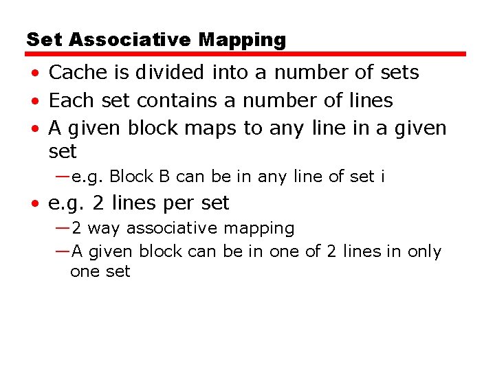
Set Associative Mapping • Cache is divided into a number of sets • Each set contains a number of lines • A given block maps to any line in a given set —e. g. Block B can be in any line of set i • e. g. 2 lines per set — 2 way associative mapping —A given block can be in one of 2 lines in only one set

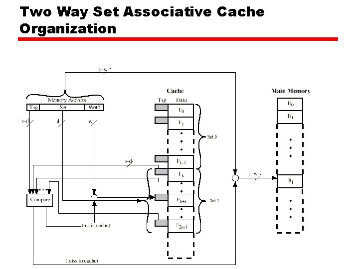
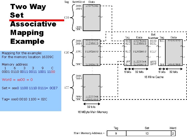
Two Way Set Associative Cache Organization

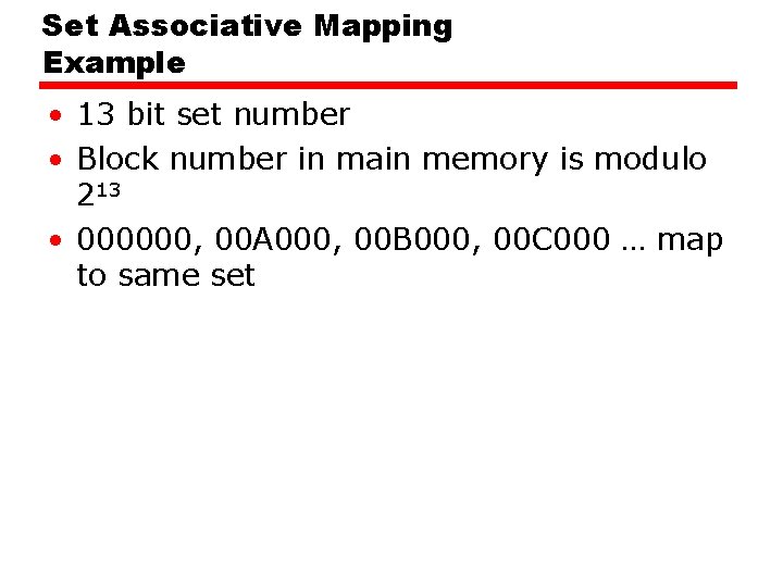
Set Associative Mapping Example • 13 bit set number • Block number in main memory is modulo 213 • 000000, 00 A 000, 00 B 000, 00 C 000 … map to same set

Two Way Set Associative Mapping Example Mapping for the example: For the memory location 16339 C Memory address 1 6 3 3 9 C 0001 0110 0011 1001 1100 Word = 0000 =0 Set = 0000 1110 0111= 0 CE 7 Tag= 0000 0010 1100 = 02 C

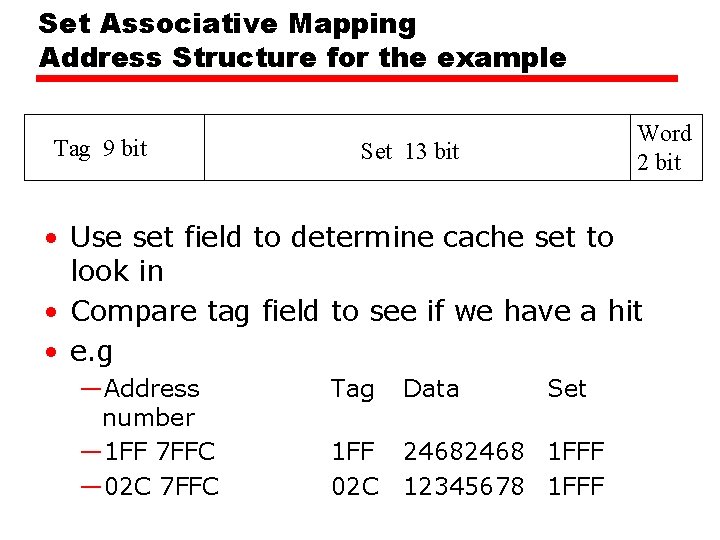
Set Associative Mapping Address Structure for the example Tag 9 bit Word 2 bit Set 13 bit • Use set field to determine cache set to look in • Compare tag field to see if we have a hit • e. g —Address number — 1 FF 7 FFC — 02 C 7 FFC Tag Data Set 1 FF 02 C 2468 1 FFF 12345678 1 FFF

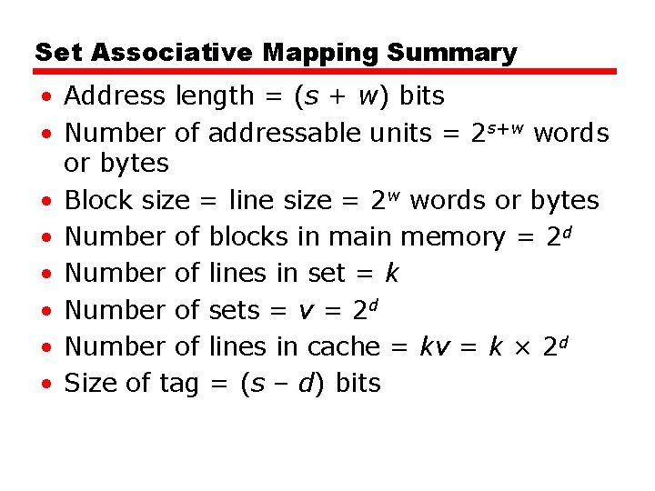
Set Associative Mapping Summary • Address length = (s + w) bits • Number of addressable units = 2 s+w words or bytes • Block size = line size = 2 w words or bytes • Number of blocks in main memory = 2 d • Number of lines in set = k • Number of sets = v = 2 d • Number of lines in cache = kv = k × 2 d • Size of tag = (s – d) bits

Replacement Algorithms (1) Direct mapping • No choice • Each block only maps to one line • Replace that line

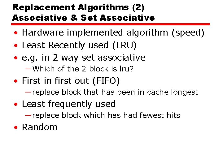
Replacement Algorithms (2) Associative & Set Associative • Hardware implemented algorithm (speed) • Least Recently used (LRU) • e. g. in 2 way set associative —Which of the 2 block is lru? • First in first out (FIFO) —replace block that has been in cache longest • Least frequently used —replace block which has had fewest hits • Random

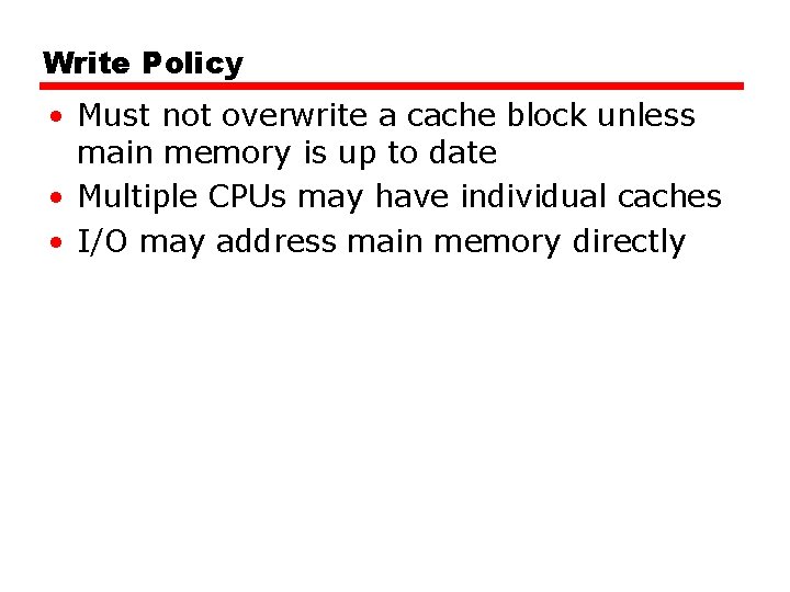
Write Policy • Must not overwrite a cache block unless main memory is up to date • Multiple CPUs may have individual caches • I/O may address main memory directly

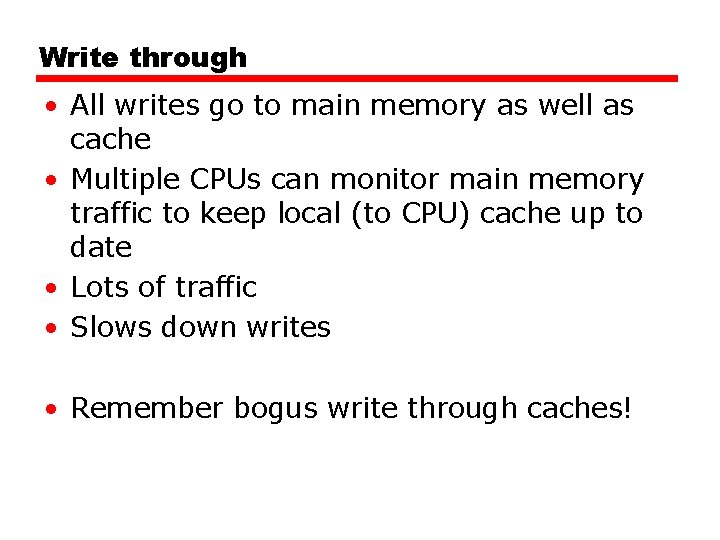
Write through • All writes go to main memory as well as cache • Multiple CPUs can monitor main memory traffic to keep local (to CPU) cache up to date • Lots of traffic • Slows down writes • Remember bogus write through caches!

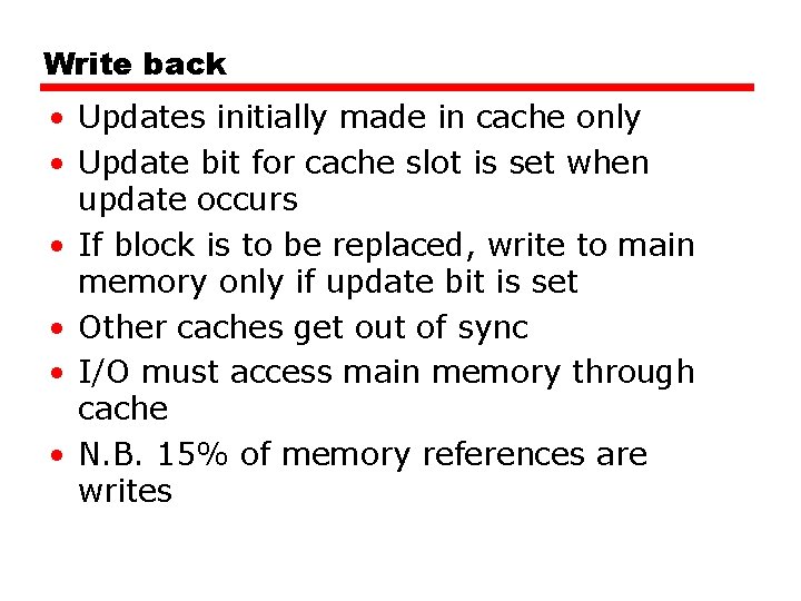
Write back • Updates initially made in cache only • Update bit for cache slot is set when update occurs • If block is to be replaced, write to main memory only if update bit is set • Other caches get out of sync • I/O must access main memory through cache • N. B. 15% of memory references are writes

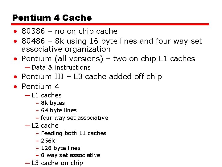
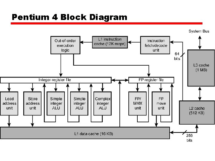
Pentium 4 Cache • 80386 – no on chip cache • 80486 – 8 k using 16 byte lines and four way set associative organization • Pentium (all versions) – two on chip L 1 caches — Data & instructions • Pentium III – L 3 cache added off chip • Pentium 4 — L 1 caches – 8 k bytes – 64 byte lines – four way set associative — L 2 cache – – Feeding both L 1 caches 256 k 128 byte lines 8 way set associative — L 3 cache on chip

Pentium 4 Block Diagram

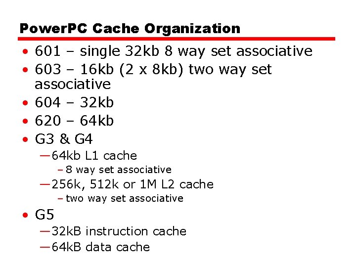
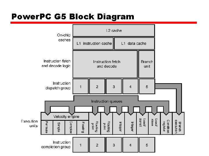
Power. PC Cache Organization • 601 – single 32 kb 8 way set associative • 603 – 16 kb (2 x 8 kb) two way set associative • 604 – 32 kb • 620 – 64 kb • G 3 & G 4 — 64 kb L 1 cache – 8 way set associative — 256 k, 512 k or 1 M L 2 cache – two way set associative • G 5 — 32 k. B instruction cache — 64 k. B data cache

Power. PC G 5 Block Diagram

Virtual Memory • Cache memory enhances performance by providing faster memory access speed. • Virtual memory enhances performance by providing greater memory capacity, without the expense of adding main memory. • Instead, a portion of a disk drive serves as an extension of main memory. • If a system uses paging, virtual memory partitions main memory into individually managed page frames, that are written (or paged) to disk when they are not immediately needed.

Virtual Memory • A physical address is the actual memory address of physical memory. • Programs create virtual addresses that are mapped to physical addresses by the memory manager. • Page faults occur when a logical address requires that a page be brought in from disk. • Memory fragmentation occurs when the paging process results in the creation of small, unusable clusters of memory addresses.

Virtual Memory • Main memory and virtual memory are divided into equal sized pages. • The entire address space required by a process need not be in memory at once. Some parts can be on disk, while others are in main memory. • Further, the pages allocated to a process do not need to be stored contiguously-- either on disk or in memory. • In this way, only the needed pages are in memory at any time, the unnecessary pages are in slower disk storage.

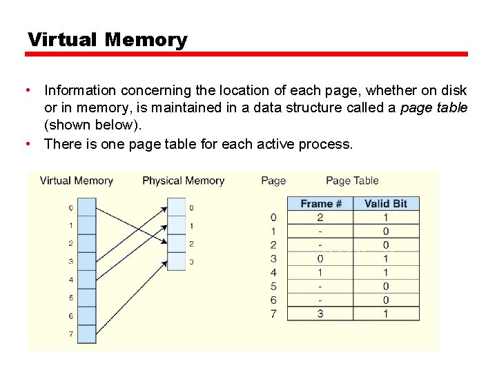
Virtual Memory • Information concerning the location of each page, whether on disk or in memory, is maintained in a data structure called a page table (shown below). • There is one page table for each active process.

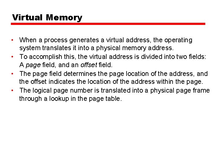
Virtual Memory • When a process generates a virtual address, the operating system translates it into a physical memory address. • To accomplish this, the virtual address is divided into two fields: A page field, and an offset field. • The page field determines the page location of the address, and the offset indicates the location of the address within the page. • The logical page number is translated into a physical page frame through a lookup in the page table.

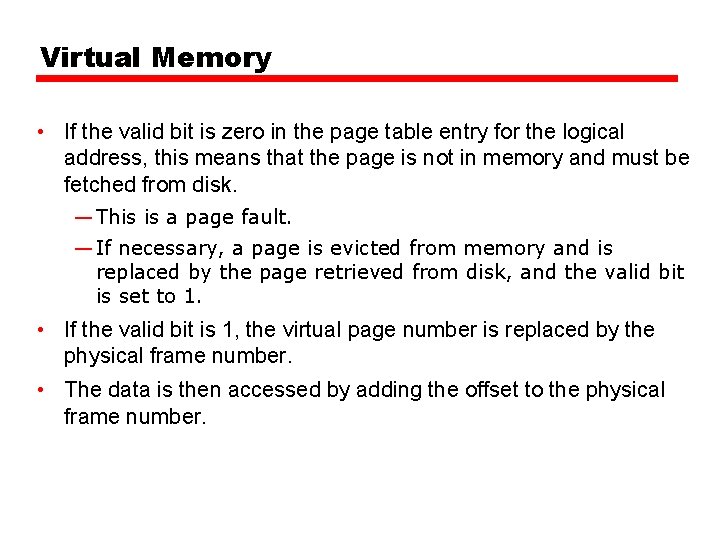
Virtual Memory • If the valid bit is zero in the page table entry for the logical address, this means that the page is not in memory and must be fetched from disk. — This is a page fault. — If necessary, a page is evicted from memory and is replaced by the page retrieved from disk, and the valid bit is set to 1. • If the valid bit is 1, the virtual page number is replaced by the physical frame number. • The data is then accessed by adding the offset to the physical frame number.

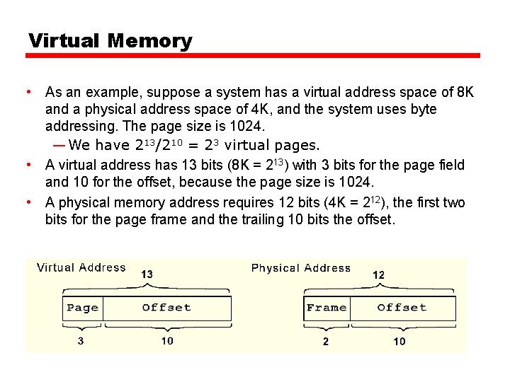
Virtual Memory • As an example, suppose a system has a virtual address space of 8 K and a physical address space of 4 K, and the system uses byte addressing. The page size is 1024. — We have 213/210 = 23 virtual pages. • A virtual address has 13 bits (8 K = 213) with 3 bits for the page field and 10 for the offset, because the page size is 1024. • A physical memory address requires 12 bits (4 K = 212), the first two bits for the page frame and the trailing 10 bits the offset.

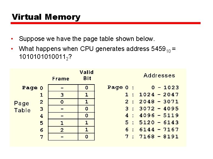
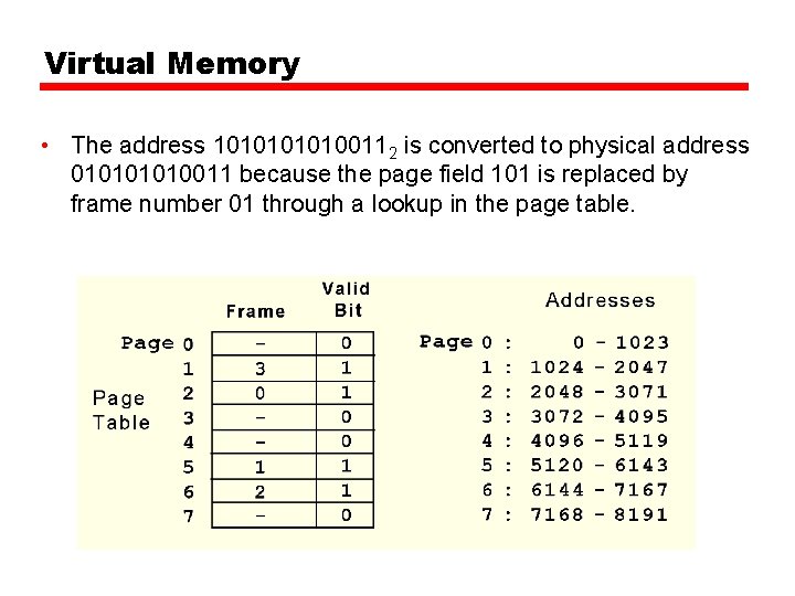
Virtual Memory • Suppose we have the page table shown below. • What happens when CPU generates address 545910 = 1010100112?

Virtual Memory • The address 1010100112 is converted to physical address 01010011 because the page field 101 is replaced by frame number 01 through a lookup in the page table.

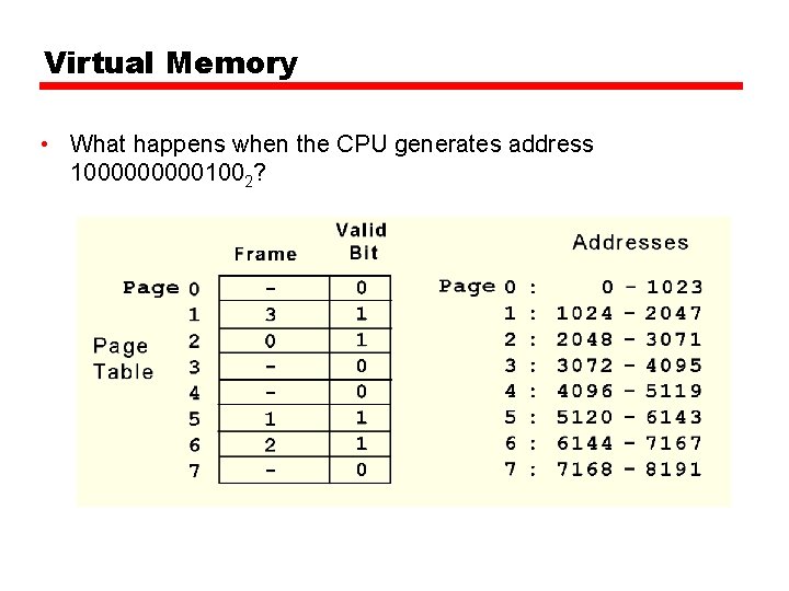
Virtual Memory • What happens when the CPU generates address 1000001002? If the valid bit is zero in the page table entry for the logical address, this means that the page is not in memory and must be fetched from disk. This is a page fault. If necessary, a page is evicted from memory and is replaced by the page retrieved from disk, and the valid bit is set to 1.

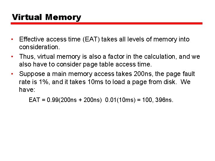
Virtual Memory • Effective access time (EAT) takes all levels of memory into consideration. • Thus, virtual memory is also a factor in the calculation, and we also have to consider page table access time. • Suppose a main memory access takes 200 ns, the page fault rate is 1%, and it takes 10 ms to load a page from disk. We have: EAT = 0. 99(200 ns + 200 ns) 0. 01(10 ms) = 100, 396 ns.

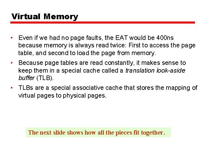
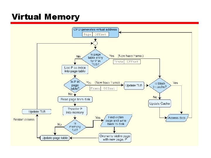
Virtual Memory • Even if we had no page faults, the EAT would be 400 ns because memory is always read twice: First to access the page table, and second to load the page from memory. • Because page tables are read constantly, it makes sense to keep them in a special cache called a translation look-aside buffer (TLB). • TLBs are a special associative cache that stores the mapping of virtual pages to physical pages. The next slide shows how all the pieces fit together.

Virtual Memory

Virtual Memory • Another approach to virtual memory is the use of segmentation. • Instead of dividing memory into equal-sized pages, virtual address space is divided into variable-length segments, often under the control of the programmer. • A segment is located through its entry in a segment table, which contains the segment’s memory location and a bounds limit that indicates its size. • After a page fault, the operating system searches for a location in memory large enough to hold the segment that is retrieved from disk.

Virtual Memory • Both paging and segmentation cause fragmentation. • Paging is subject to internal fragmentation because a process may not need the entire range of addresses contained within the page. Thus, there may be many pages containing unused fragments of memory. • Segmentation is subject to external fragmentation, which occurs when contiguous chunks of memory become broken up as segments are allocated and deallocated over time.

Virtual Memory • Large page tables are cumbersome and slow, but with its uniform memory mapping, page operations are fast. Segmentation allows fast access to the segment table, but segment loading is labor-intensive. • Paging and segmentation can be combined to take advantage of the best features of both by assigning fixed-size pages within variable-sized segments. • Each segment has a page table. This means that a memory address will have three fields, one for the segment, another for the page, and a third for the offset.

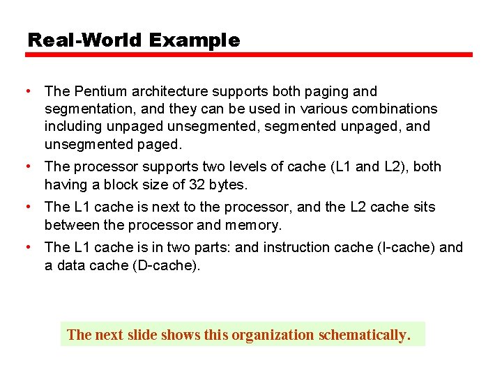
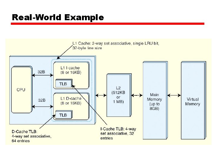
Real-World Example • The Pentium architecture supports both paging and segmentation, and they can be used in various combinations including unpaged unsegmented, segmented unpaged, and unsegmented paged. • The processor supports two levels of cache (L 1 and L 2), both having a block size of 32 bytes. • The L 1 cache is next to the processor, and the L 2 cache sits between the processor and memory. • The L 1 cache is in two parts: and instruction cache (I-cache) and a data cache (D-cache). The next slide shows this organization schematically.

Real-World Example

Semiconductor Memory Types

Semiconductor Memory • RAM —Misnamed as all semiconductor memory is random access —Read/Write —Volatile —Temporary storage —Static or dynamic

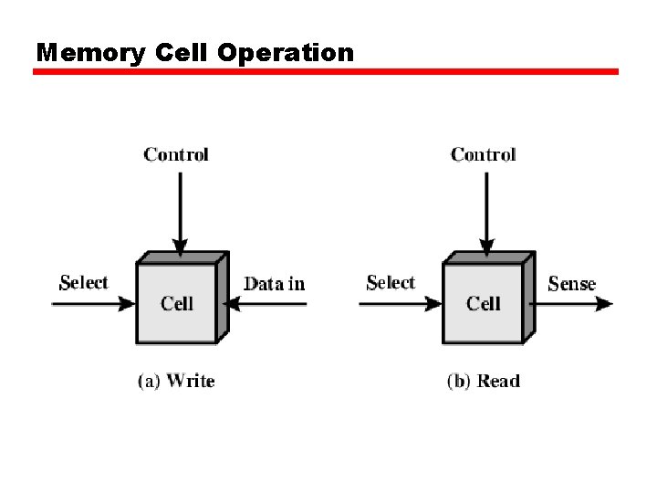
Memory Cell Operation

Dynamic RAM • • • Bits stored as charge in capacitors Charges leak Need refreshing even when powered Simpler construction Smaller per bit Less expensive Need refresh circuits Slower Main memory Essentially analogue — Level of charge determines value

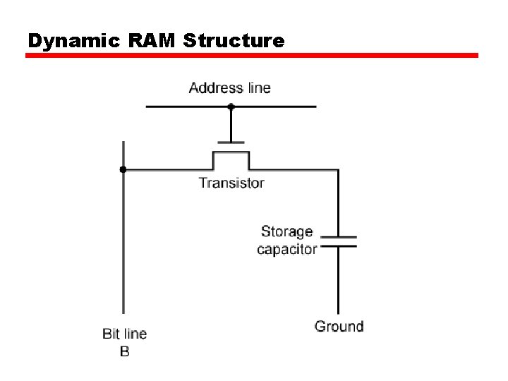
Dynamic RAM Structure

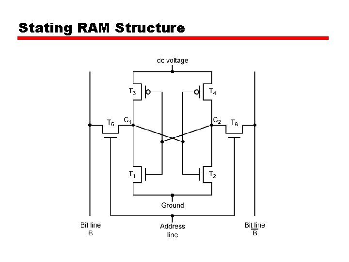
Static RAM • • • Bits stored as on/off switches No charges to leak No refreshing needed when powered More complex construction Larger per bit More expensive Does not need refresh circuits Faster Cache Digital — Uses flip-flops

Stating RAM Structure

SRAM v DRAM • Both volatile — Power needed to preserve data • Dynamic cell — Simpler to build, smaller — More dense — Less expensive — Needs refresh — Larger memory units • Static — Faster — Cache

Advanced DRAM Organization • Basic DRAM same since first RAM chips • Enhanced DRAM —Contains small SRAM as well —SRAM holds last line read (c. f. Cache!) • Cache DRAM —Larger SRAM component —Use as cache or serial buffer

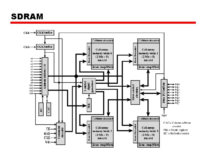
Synchronous DRAM (SDRAM) • • Access is synchronized with an external clock Address is presented to RAM finds data (CPU waits in conventional DRAM) Since SDRAM moves data in time with system clock, CPU knows when data will be ready • CPU does not have to wait, it can do something else • Burst mode allows SDRAM to set up stream of data and fire it out in block • DDR-SDRAM sends data twice per clock cycle (leading & trailing edge)

SDRAM

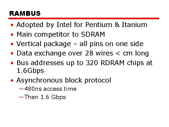
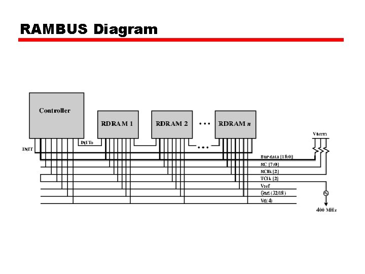
RAMBUS • • • Adopted by Intel for Pentium & Itanium Main competitor to SDRAM Vertical package – all pins on one side Data exchange over 28 wires < cm long Bus addresses up to 320 RDRAM chips at 1. 6 Gbps • Asynchronous block protocol — 480 ns access time —Then 1. 6 Gbps

RAMBUS Diagram

DDR SDRAM • SDRAM can only send data once per clock • Double-data-rate SDRAM can send data twice per clock cycle —Rising edge and falling edge

Cache DRAM • Mitsubishi • Integrates small SRAM cache (16 kb) onto generic DRAM chip • Used as true cache — 64 -bit lines —Effective for ordinary random access • To support serial access of block of data —E. g. refresh bit-mapped screen – CDRAM can prefetch data from DRAM into SRAM buffer – Subsequent accesses solely to SRAM

Read Only Memory (ROM) • Permanent storage —Nonvolatile • Used in. . . —Microprogramming —Library subroutines —Systems programs (BIOS) —Function tables

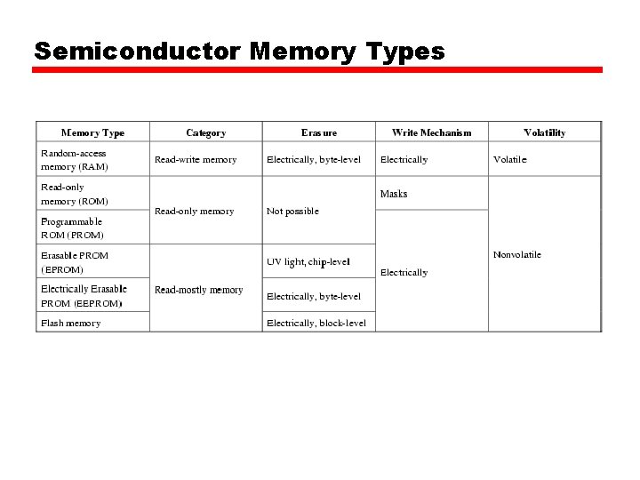
Types of ROM • Written during manufacture — Very expensive for small runs • Programmable (once) — PROM — Needs special equipment to program • Read “mostly” — Erasable Programmable (EPROM) – Erased by UV — Electrically Erasable (EEPROM) – Takes much longer to write than read — Flash memory – Erase whole memory electrically

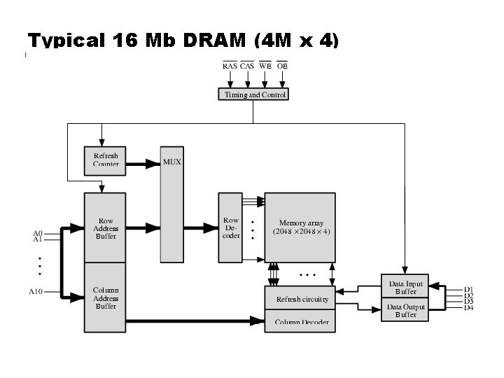
Organisation in detail • A 16 Mbit chip can be organised as 1 M of 16 bit words • A bit per chip system has 16 lots of 1 Mbit chip with bit 1 of each word in chip 1 and so on • A 16 Mbit chip can be organised as a 2048 x 4 bit array —Reduces number of address pins – Multiplex row address and column address – 11 pins to address (211=2048) – Adding one more pin doubles range of values so x 4 capacity

Typical 16 Mb DRAM (4 M x 4)

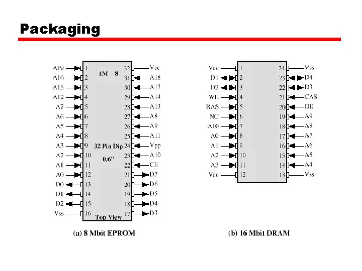
Packaging

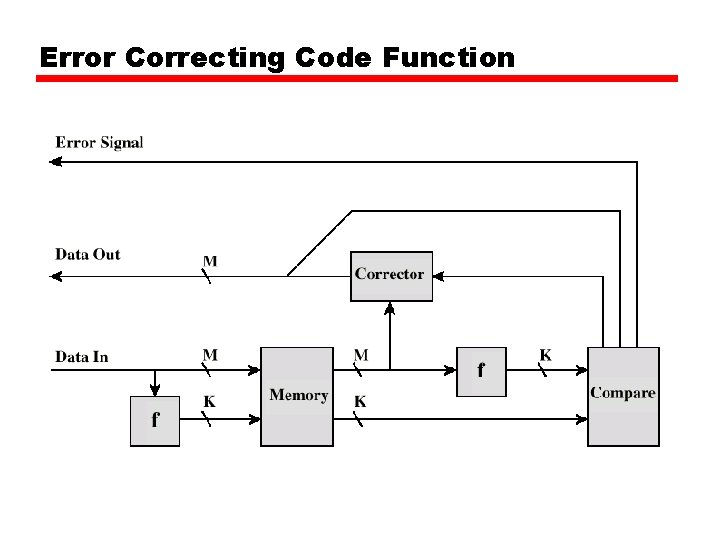
Error Correction • Hard Failure —Permanent defect • Soft Error —Random, non-destructive —No permanent damage to memory • Detected using Hamming error correcting code

Error Correcting Code Function