From Design to Design Automation Jason Cong Chancellors

![x. Pilot: Behavioral-to-RTL Synthesis Flow [SOCC’ 2006] Behavioral spec. in C/C++/System. C Platform description x. Pilot: Behavioral-to-RTL Synthesis Flow [SOCC’ 2006] Behavioral spec. in C/C++/System. C Platform description](https://slidetodoc.com/presentation_image_h2/ab4a6f25568345bdff1b151adb9f76fd/image-32.jpg)

- Slides: 40

From Design to Design Automation Jason Cong Chancellor’s Professor, UCLA Director, Center for Domain-Specific Computing cong@cs. ucla. edu http: //cadlab. cs. ucla. edu/~cong 1

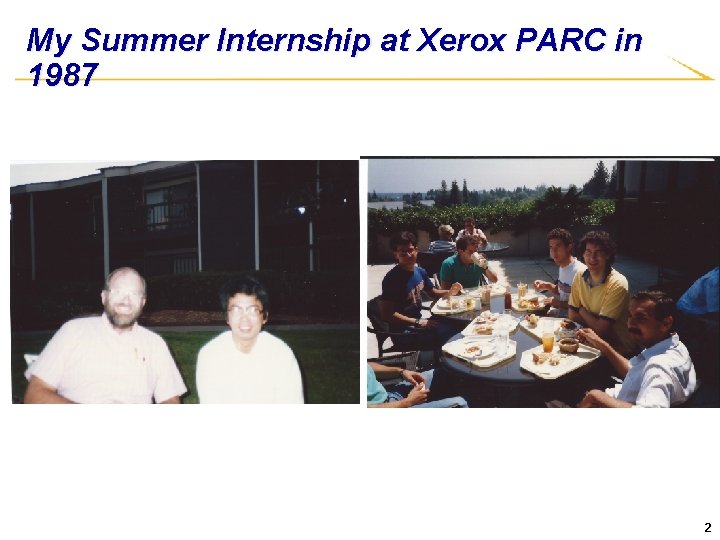
My Summer Internship at Xerox PARC in 1987 2

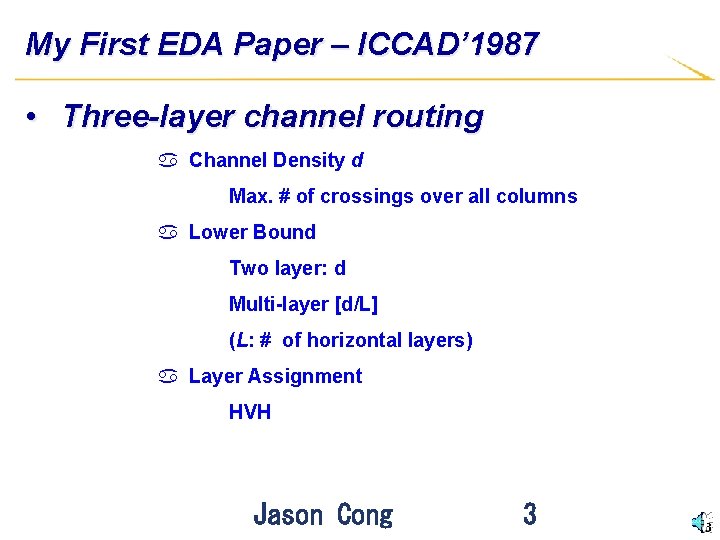
My First EDA Paper – ICCAD’ 1987 • Three-layer channel routing a Channel Density d Max. # of crossings over all columns a Lower Bound Two layer: d Multi-layer [d/L] (L: # of horizontal layers) a Layer Assignment HVH Jason Cong 3 3

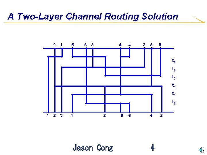
A Two-Layer Channel Routing Solution 2 1 5 6 3 4 4 3 2 5 t 1 t 2 t 3 t 4 t 5 t 6 1 2 3 4 2 Jason Cong 6 6 4 4 2 4

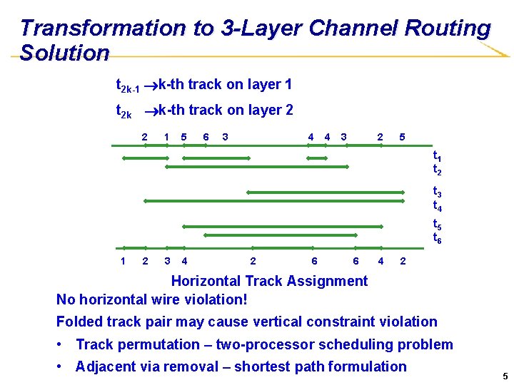
Transformation to 3 -Layer Channel Routing Solution t 2 k-1 k-th track on layer 1 t 2 k k-th track on layer 2 2 1 5 6 3 4 4 3 2 5 t 1 t 2 t 3 t 4 t 5 t 6 1 2 3 4 2 6 6 4 2 Horizontal Track Assignment No horizontal wire violation! Folded track pair may cause vertical constraint violation • Track permutation – two-processor scheduling problem • Adjacent via removal – shortest path formulation 5

My First Month at PARC u. I was eager to apply combinatorial optimization techniques to more physical design problems … u But Bryan asked me to learn to use the DATools to do a design u DATools at Xerox PARC was state-of-art § HDL specification and schematic entry § Floorplan § Placement § Global routing § Details routing § DRC and LVS … u All written in objected oriented programming style 6

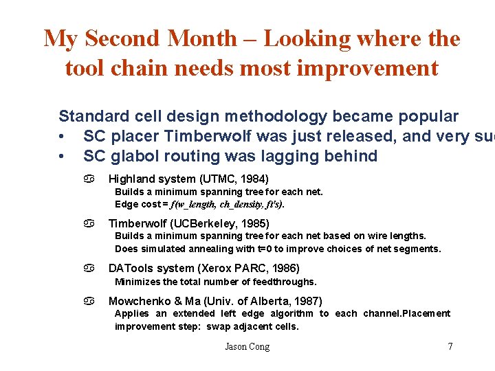
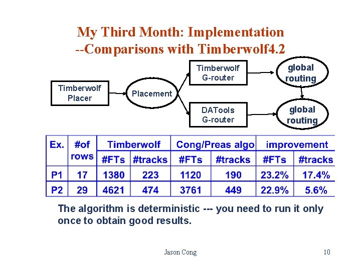
My Second Month – Looking where the tool chain needs most improvement Standard cell design methodology became popular • SC placer Timberwolf was just released, and very suc • SC glabol routing was lagging behind a Highland system (UTMC, 1984) Builds a minimum spanning tree for each net. Edge cost = f(w_length, ch_density, ft's). a Timberwolf (UCBerkeley, 1985) Builds a minimum spanning tree for each net based on wire lengths. Does simulated annealing with t=0 to improve choices of net segments. a DATools system (Xerox PARC, 1986) Minimizes the total number of feedthroughs. a Mowchenko & Ma (Univ. of Alberta, 1987) Applies an extended left edge algorithm to each channel. Placement improvement step: swap adjacent cells. Jason Cong 7

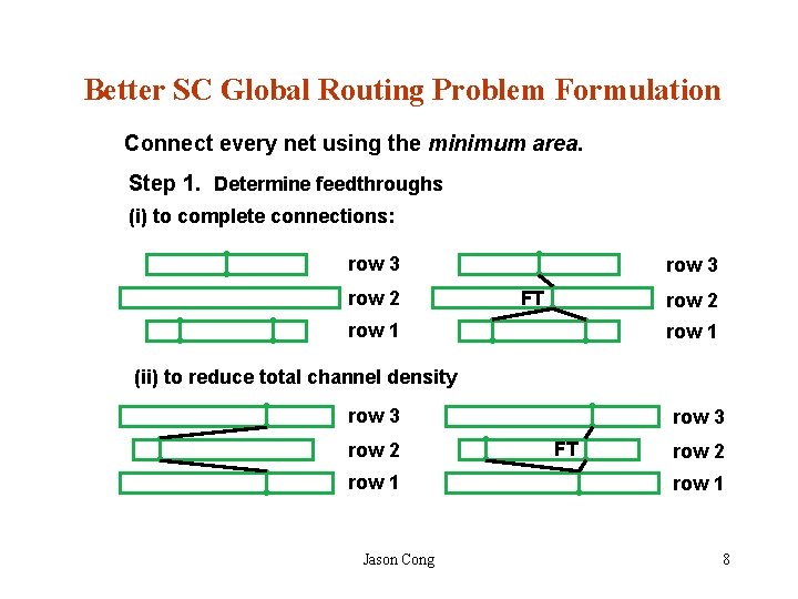
Better SC Global Routing Problem Formulation Connect every net using the minimum area. Step 1. Determine feedthroughs (i) to complete connections: row 3 row 2 row 3 FT row 2 row 1 (ii) to reduce total channel density row 3 row 2 row 1 Jason Cong row 3 FT row 2 row 1 8

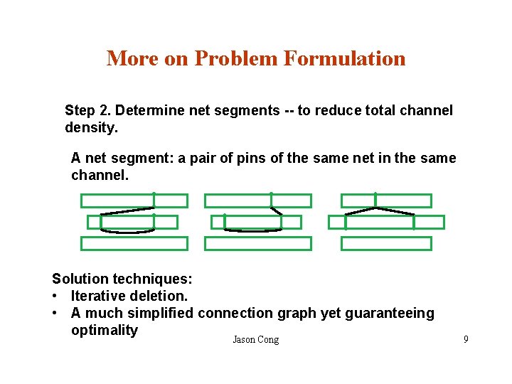
More on Problem Formulation Step 2. Determine net segments -- to reduce total channel density. A net segment: a pair of pins of the same net in the same channel. Solution techniques: • Iterative deletion. • A much simplified connection graph yet guaranteeing optimality Jason Cong 9

My Third Month: Implementation --Comparisons with Timberwolf 4. 2 Timberwolf Placer Timberwolf G-router global routing DATools G-router global routing Placement The algorithm is deterministic --- you need to run it only once to obtain good results. Jason Cong 10

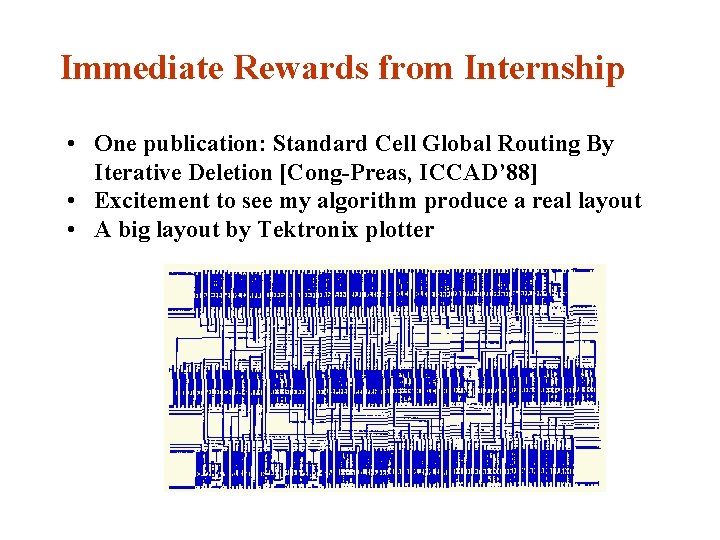
Immediate Rewards from Internship • One publication: Standard Cell Global Routing By Iterative Deletion [Cong-Preas, ICCAD’ 88] • Excitement to see my algorithm produce a real layout • A big layout by Tektronix plotter

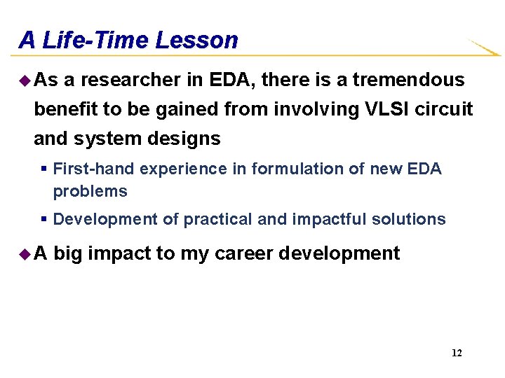
A Life-Time Lesson u As a researcher in EDA, there is a tremendous benefit to be gained from involving VLSI circuit and system designs § First-hand experience in formulation of new EDA problems § Development of practical and impactful solutions u. A big impact to my career development 12

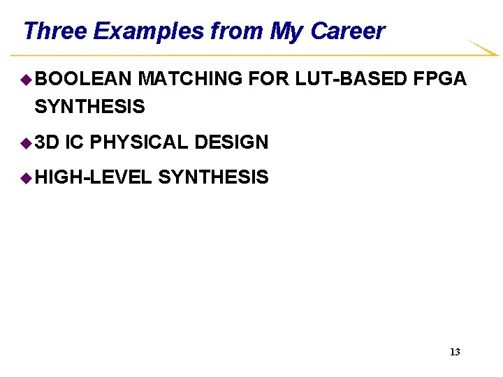
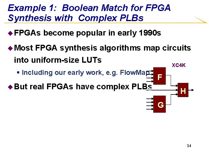
Three Examples from My Career u BOOLEAN MATCHING FOR LUT-BASED FPGA SYNTHESIS u 3 D IC PHYSICAL DESIGN u HIGH-LEVEL SYNTHESIS 13

Example 1: Boolean Match for FPGA Synthesis with Complex PLBs u FPGAs become popular in early 1990 s u Most FPGA synthesis algorithms map circuits into uniform-size LUTs XC 4 K § Including our early work, e. g. Flow. Map u But F real FPGAs have complex PLBsx H G 14

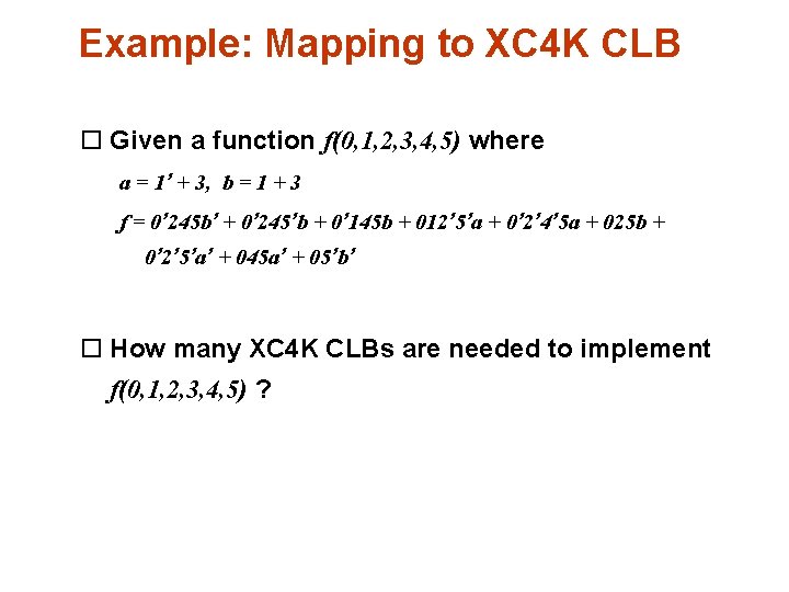
Example: Mapping to XC 4 K CLB o Given a function f(0, 1, 2, 3, 4, 5) where a = 1’ + 3, b = 1 + 3 f = 0’ 245 b’ + 0’ 245’b + 0’ 145 b + 012’ 5’a + 0’ 2’ 4’ 5 a + 025 b + 0’ 2’ 5’a’ + 045 a’ + 05’b’ o How many XC 4 K CLBs are needed to implement f(0, 1, 2, 3, 4, 5) ?

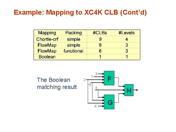
Example: Mapping to XC 4 K CLB (Cont’d) The Boolean matching result 2 1 0 3 F 5 4 H G

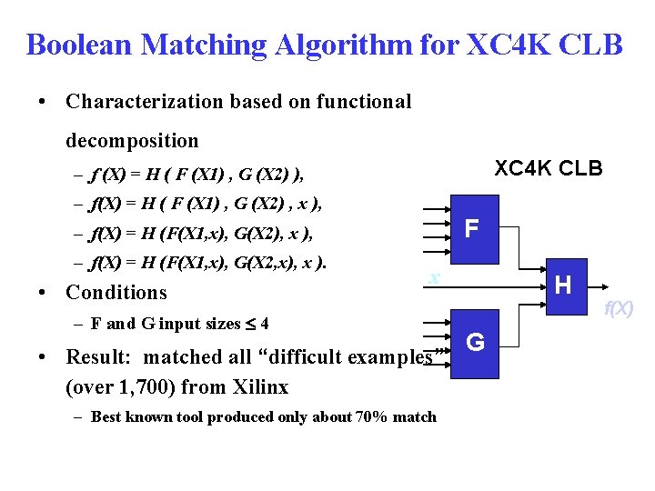
Boolean Matching Algorithm for XC 4 K CLB • Characterization based on functional decomposition XC 4 K CLB – f (X) = H ( F (X 1) , G (X 2) ), – f(X) = H ( F (X 1) , G (X 2) , x ), F – f(X) = H (F(X 1, x), G(X 2), x ), – f(X) = H (F(X 1, x), G(X 2, x), x ). • Conditions x – F and G input sizes 4 • Result: matched all “difficult examples” (over 1, 700) from Xilinx – Best known tool produced only about 70% match H G f(X)

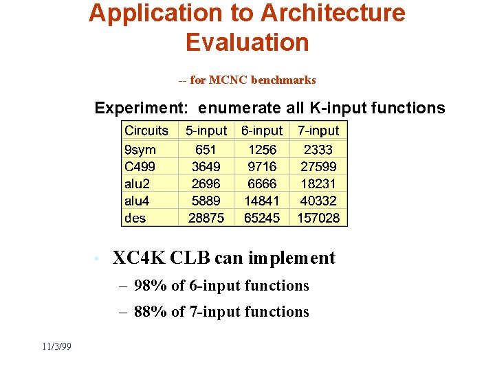
Application to Architecture Evaluation -- for MCNC benchmarks Experiment: enumerate all K-input functions • XC 4 K CLB can implement – 98% of 6 -input functions – 88% of 7 -input functions 11/3/99

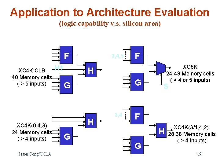
Application to Architecture Evaluation (logic capability v. s. silicon area) F XC 4 K CLB 40 Memory cells ( > 5 inputs) XC 4 K(0, 4, 3) 24 Memory cells ( > 4 inputs) Jason Cong/UCLA H 1 3, 4, 5 F XC 5 K 24 -48 Memory cells ( > 4 or 5 inputs) H G G H G 3, 4 S F H G XC 4 K(3/4, 4, 2) 28, 36 Memory cells ( > 4 inputs) 19

Example 2: 3 D IC Physical Design • Motivations – DARPA wanted to demonstrate 3 D IC technology – Intel wanted to understand the benefit of 3 D architectures

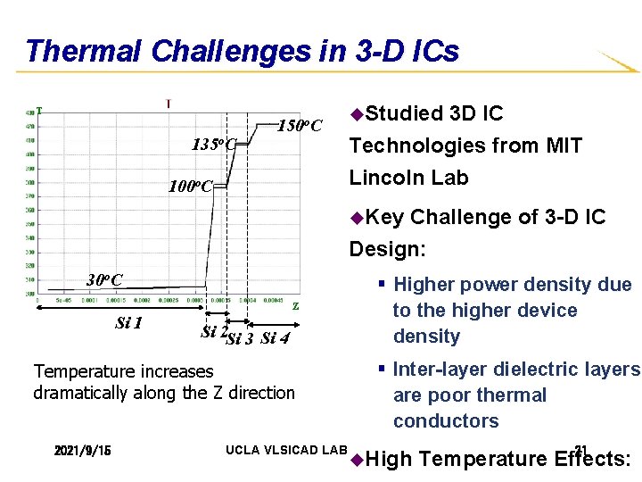
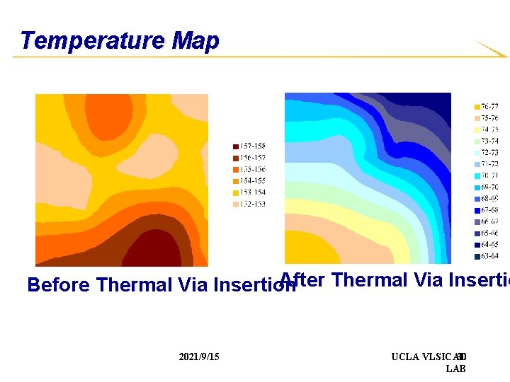
Thermal Challenges in 3 -D ICs T 135 o. C 150 o. C 100 o. C u. Studied 3 D IC Technologies from MIT Lincoln Lab u. Key Challenge of 3 -D IC Design: 30 o. C Z Si 1 Si 2 Si 3 Si 4 Temperature increases dramatically along the Z direction 2021/9/15 UCLA VLSICAD LAB § Higher power density due to the higher device density § Inter-layer dielectric layers are poor thermal conductors u. High 21 Temperature Effects:

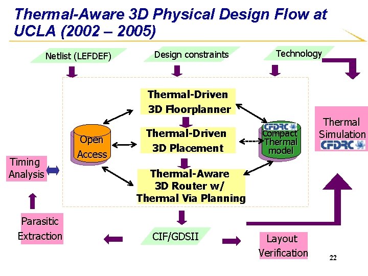
Thermal-Aware 3 D Physical Design Flow at UCLA (2002 – 2005) Netlist (LEFDEF) Design constraints Technology Thermal-Driven 3 D Floorplanner Timing Analysis Parasitic Extraction Open Access Thermal-Driven 3 D Placement Compact Thermal model Thermal Simulation Thermal-Aware 3 D Router w/ Thermal Via Planning CIF/GDSII Layout Verification 22

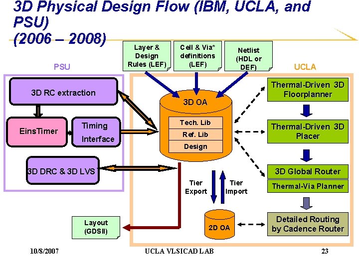
3 D Physical Design Flow (IBM, UCLA, and PSU) (2006 – 2008) Layer & Cell & Via* Design Rules (LEF) PSU Netlist (HDL or DEF) definitions (LEF) Thermal-Driven 3 D Floorplanner 3 D RC extraction 3 D OA Eins. Timer Timing Interface Tech. Lib Thermal-Driven 3 D Placer Ref. Lib Design 3 D Global Router 3 D DRC & 3 D LVS Tier Export Layout (GDSII) 10/8/2007 UCLA Tier Import 2 D OA UCLA VLSICAD LAB Thermal-Via Planner Detailed Routing by Cadence Router 23

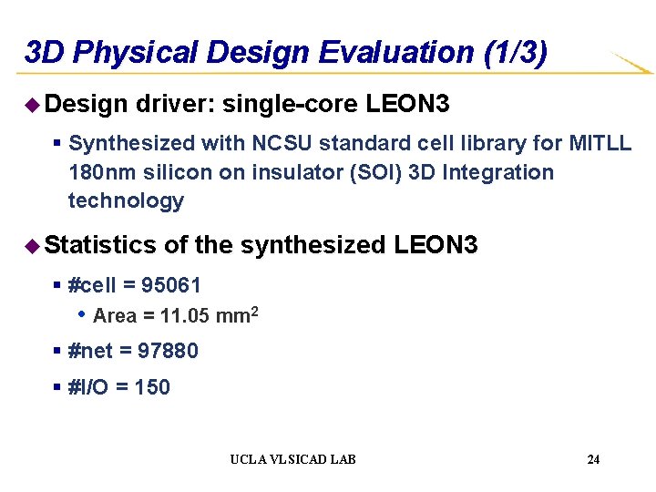
3 D Physical Design Evaluation (1/3) u Design driver: single-core LEON 3 § Synthesized with NCSU standard cell library for MITLL 180 nm silicon on insulator (SOI) 3 D Integration technology u Statistics of the synthesized LEON 3 § #cell = 95061 • Area = 11. 05 mm 2 § #net = 97880 § #I/O = 150 UCLA VLSICAD LAB 24

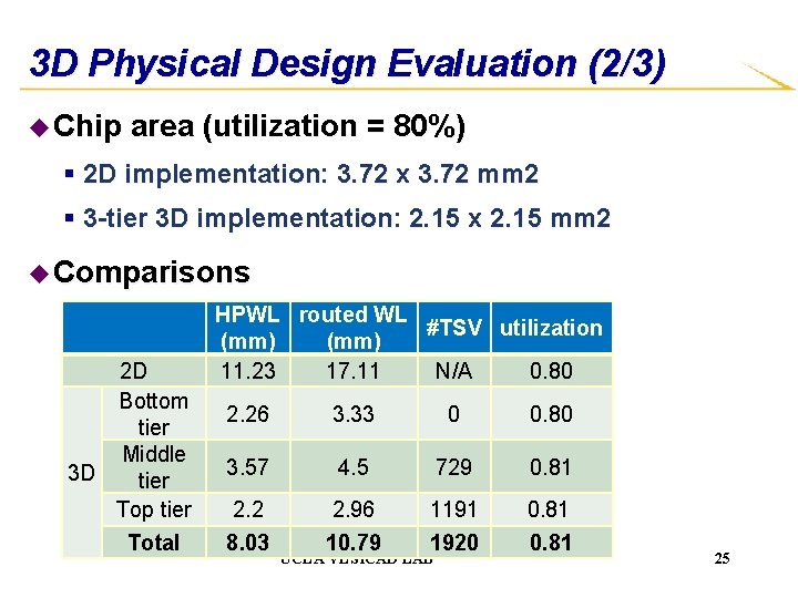
3 D Physical Design Evaluation (2/3) u Chip area (utilization = 80%) § 2 D implementation: 3. 72 x 3. 72 mm 2 § 3 -tier 3 D implementation: 2. 15 x 2. 15 mm 2 u Comparisons 2 D Bottom tier Middle 3 D tier Top tier Total HPWL routed WL #TSV utilization (mm) 11. 23 17. 11 N/A 0. 80 2. 26 3. 33 0 0. 80 3. 57 4. 5 729 0. 81 2. 2 8. 03 2. 96 10. 79 1191 1920 0. 81 UCLA VLSICAD LAB 25

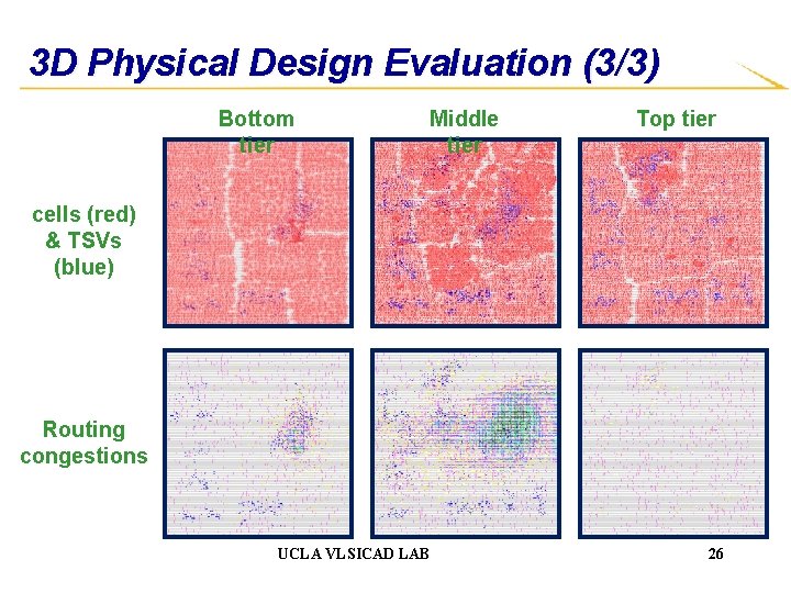
3 D Physical Design Evaluation (3/3) Bottom tier Middle tier Top tier cells (red) & TSVs (blue) Routing congestions UCLA VLSICAD LAB 26

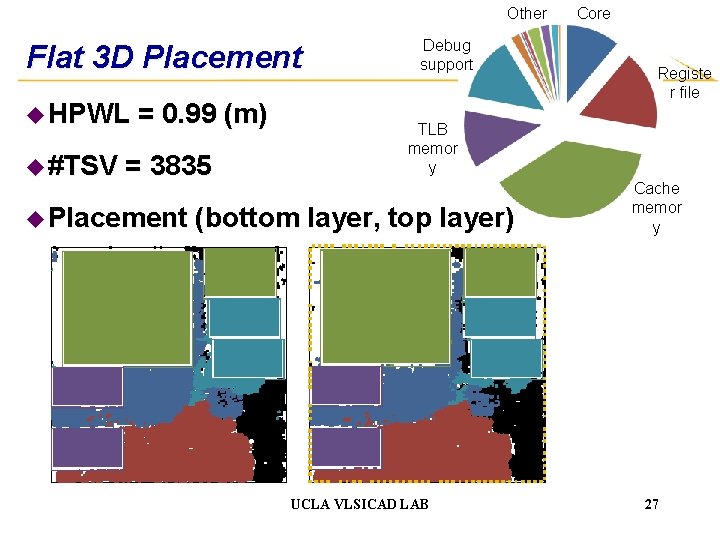
Other Flat 3 D Placement u HPWL u #TSV = 0. 99 (m) = 3835 u Placement Debug support Core Registe r file TLB memor y (bottom layer, top layer) UCLA VLSICAD LAB Cache memor y 27

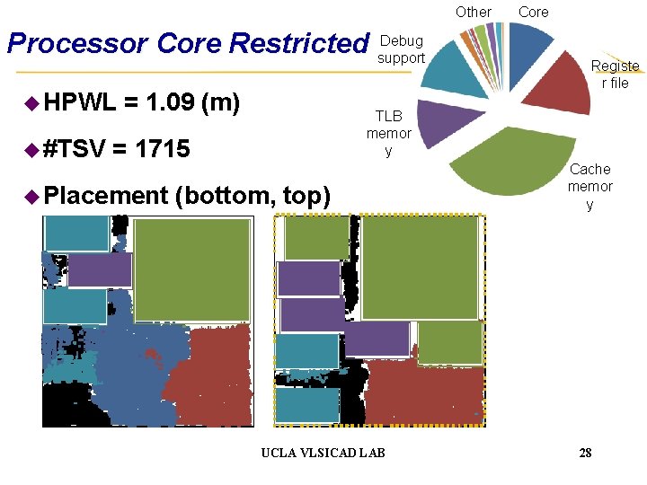
Other Debug Processor Core Restricted support u HPWL u #TSV = 1. 09 (m) Registe r file TLB memor y = 1715 u Placement Core (bottom, top) UCLA VLSICAD LAB Cache memor y 28

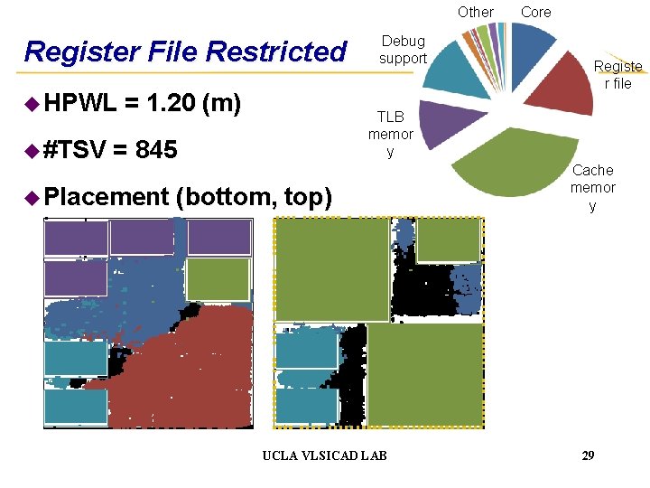
Other Register File Restricted u HPWL u #TSV = 1. 20 (m) Registe r file TLB memor y = 845 u Placement Debug support Core (bottom, top) UCLA VLSICAD LAB Cache memor y 29

Temperature Map After Thermal Via Insertio Before Thermal Via Insertion 2021/9/15 UCLA VLSICAD 30 LAB

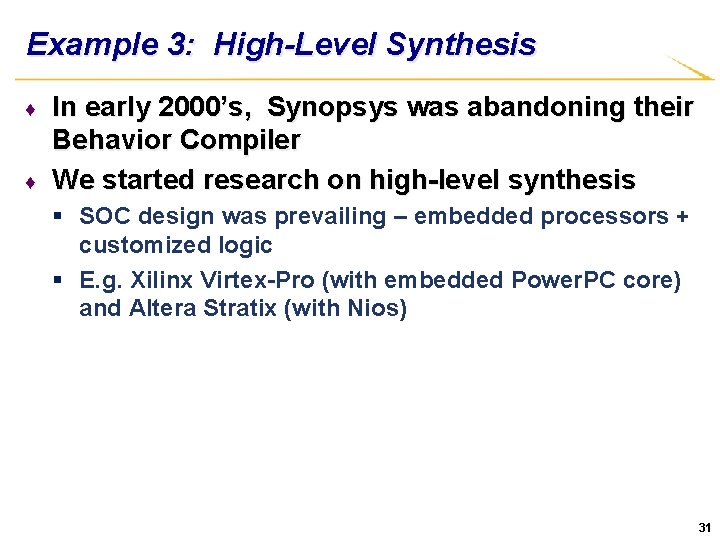
Example 3: High-Level Synthesis ♦ ♦ In early 2000’s, Synopsys was abandoning their Behavior Compiler We started research on high-level synthesis § SOC design was prevailing – embedded processors + customized logic § E. g. Xilinx Virtex-Pro (with embedded Power. PC core) and Altera Stratix (with Nios) 31
![x Pilot BehavioraltoRTL Synthesis Flow SOCC 2006 Behavioral spec in CCSystem C Platform description x. Pilot: Behavioral-to-RTL Synthesis Flow [SOCC’ 2006] Behavioral spec. in C/C++/System. C Platform description](https://slidetodoc.com/presentation_image_h2/ab4a6f25568345bdff1b151adb9f76fd/image-32.jpg)
x. Pilot: Behavioral-to-RTL Synthesis Flow [SOCC’ 2006] Behavioral spec. in C/C++/System. C Platform description Frontend compiler (LLVM) u Code transformation & optimization § Loop unrolling/shifting/pipelining § Strength reduction / Tree height reduction § Bitwidth analysis § Memorysynthesis analysis …& u Behavior optimizations § Scheduling § Resource binding, e. g. , functional unit binding register/port binding SSDM u RTL + constraints FPGAs/ASICs Arch-generation & RTL/constraints generation § Verilog/VHDL/System. C § FPGAs: Altera, Xilinx § ASICs: Magma, Synopsys, … 32

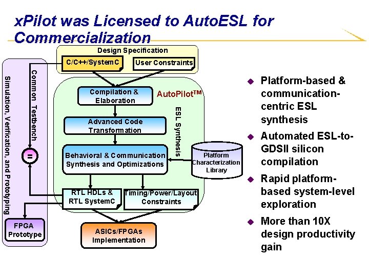
x. Pilot was Licensed to Auto. ESL for Commercialization Design Specification C/C++/System. C FPGA Prototype Compilation & Elaboration Advanced Code Transformation Behavioral & Communication Synthesis and Optimizations RTL HDLs & RTL System. C u Platform-based & communicationcentric ESL synthesis u Automated ESL-to. GDSII silicon compilation u Rapid platformbased system-level exploration u More than 10 X design productivity gain Auto. Pilot. TM ESL Synthesis Common Testbench Simulation, Verification, and Prototyping = User Constraints Platform Characterization Library Timing/Power/Layout Constraints ASICs/FPGAs Implementation

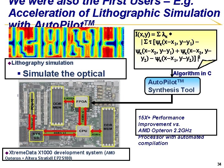
We were also the First Users – E. g. Acceleration of Lithographic Simulation with Auto. Pilot. TM u. Lithography I(x, y) = S lk * | S t [yk(x-x 1, y-y 1) yk(x-x 2, y-y 1) + yk(x-x 2, yy 2) - yk(x-x 1, y-y 2)] |2 simulation § Simulate the optical imaging process § Computational intensive; very slow for full-chip simulation u. Xtreme. Data X 1000 development Opteron + Altera Stratix. II EP 2 S 180) Algorithm in C Auto. Pilot. TM Synthesis Tool 15 X+ Performance Improvement vs. AMD Opteron 2. 2 GHz Processor with automated compilation system (AMD 34

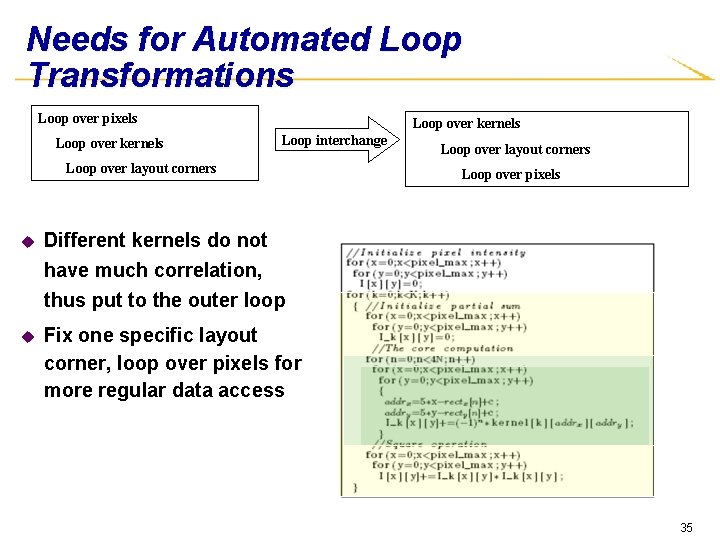
Needs for Automated Loop Transformations Loop over pixels Loop over kernels Loop interchange Loop over layout corners u Different kernels do not have much correlation, thus put to the outer loop u Fix one specific layout corner, loop over pixels for more regular data access Loop over layout corners Loop over pixels 35

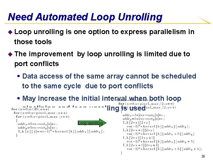
Need Automated Loop Unrolling u Loop unrolling is one option to express parallelism in those tools u The improvement by loop unrolling is limited due to port conflicts § Data access of the same array cannot be scheduled to the same cycle due to port conflicts § May increase the initial interval when both loop pipelining and loop unrolling is used Loop unrolling 36

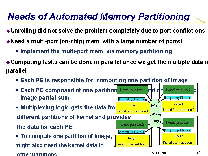
Needs of Automated Memory Partitioning u. Unrolling u. Need did not solve the problem completely due to port conflictions a multi-port (on-chip) mem with a large number of ports! § Implement the multi-port mem via memory partitioning u. Computing tasks can be done in parallel once we get the multiple data in parallel § Each PE is responsible for computing one partition of image partition 2 of Kernel partition 1 and one. Kernel § Each PE composed of one partition of kernel partition Computing Element image partial sum Computing Element Image § Multiplexing logic gets the data from Partial Sum partition 1 different partitions of kernel and provides the data for each PE Multi plexing Logic One partition Kernel partition 3 of Kernel Computing Element Image Partial Sum partition 2 Kernel partition 4 Computing Element § To compute one partition of image, One partition Imageof Image might also need the kernel data in Sum Partial Sum partition 3 Partial Sum partition 4 4 -PE example 37

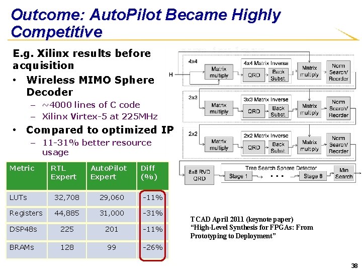
Outcome: Auto. Pilot Became Highly Competitive E. g. Xilinx results before acquisition • Wireless MIMO Sphere Decoder – ~4000 lines of C code – Xilinx Virtex-5 at 225 MHz • Compared to optimized IP – 11 -31% better resource usage Metric RTL Expert Auto. Pilot Expert Diff (%) LUTs 32, 708 29, 060 -11% Registers 44, 885 31, 000 -31% DSP 48 s 225 201 -11% BRAMs 128 99 -26% TCAD April 2011 (keynote paper) “High-Level Synthesis for FPGAs: From Prototyping to Deployment” 38

Concluding Remarks ♦ I was very fortunate to have Bryan as my mentor in my internship at Xerox PARC § Benefited immensely from Bryan’s vast experience, deep insight, and remarkable wisdom § A long-term friendship ♦ The truly important lesson that I learned from Bryan § Go from design to design automation § Gain first-hand knowledge and experience about needs from the designer’s perspective, to discover and formulate new EDA problems and develop impactful solutions. 39

Guess Where This Picture Is Taken? 40