ECE 465 Lecture Notes 1 Introduction to Digital

- Slides: 38

ECE 465 Lecture Notes # 1 Introduction to Digital Design Shantanu Dutt ECE Dept. UIC Copyright: Shantanu Dutt

Copyright: Shantanu Dutt

Copyright: Shantanu Dutt

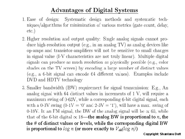
—the analog BW is proportional to n, the # of distinct values or levels, while the corresponding digital BW is proportional to log n (or more exactly to Vdd(log n)) Copyright: Shantanu Dutt

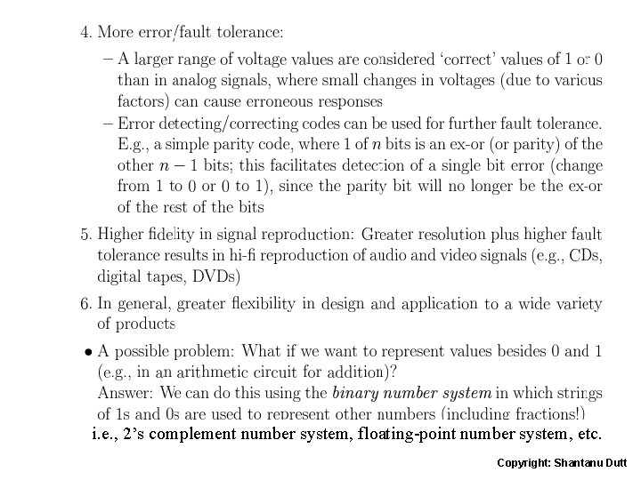
i. e. , 2’s complement number system, floating-point number system, etc. Copyright: Shantanu Dutt

Copyright: Shantanu Dutt

Copyright: Shantanu Dutt

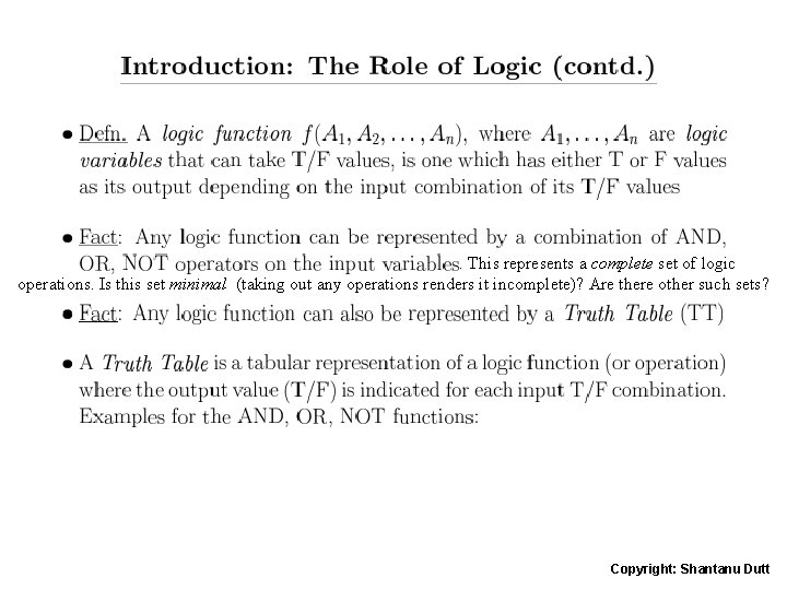
. This represents a complete set of logic operations. Is this set minimal (taking out any operations renders it incomplete)? Are there other such sets? Copyright: Shantanu Dutt

Copyright: Shantanu Dutt

Copyright: Shantanu Dutt

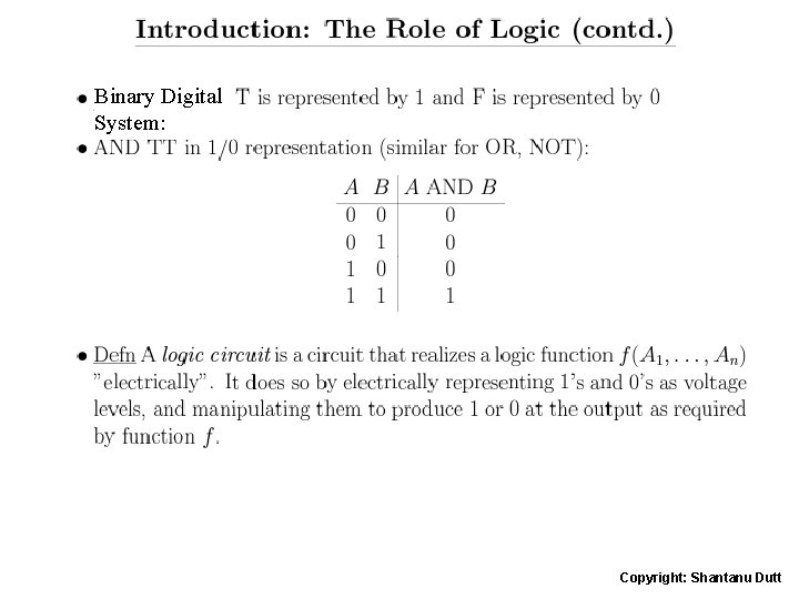
Binary Digital System: Copyright: Shantanu Dutt

Copyright: Shantanu Dutt

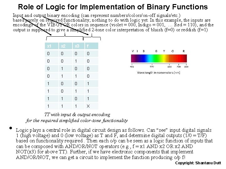
Role of Logic for Implementation of Binary Functions Input and output binary encoding (can represent numbers/colors/on-off signals/etc. ) based purely on required functionality; nothing to do with logic yet. In this example, the inputs are encodings of the VIBGYOR colors in sequence (violet = 000, Indigo = 001, … Red = 110), and the output is supposed to give a simplified 2 -tone color interpretation of bluish (f=0) or reddish (f=1) • x 1 x 2 x 3 f 0 0 0 1 1 0 0 1 1 1 1 0 1 1 X TT with input & output encoding for the required simplified color-tone functionality Logic plays a central role in digital circuit design as follows. Can “see” input digital signals 1 (high voltage) and 0 (low voltage) as T and F, and determine digital outputs (1/0 = T/F) based on functionality required. Then each o/p can be seen as a logic function of inputs that can be composed with AND/OR/NOT operators (e. g. , f = x 1 AND x 2 OR x 2 AND NOT(x 3) for above TT). Further, if we have electronic components that implement AND/OR/NOT, we can get a circuit to implement the function producing o/p f! Copyright: Shantanu Dutt

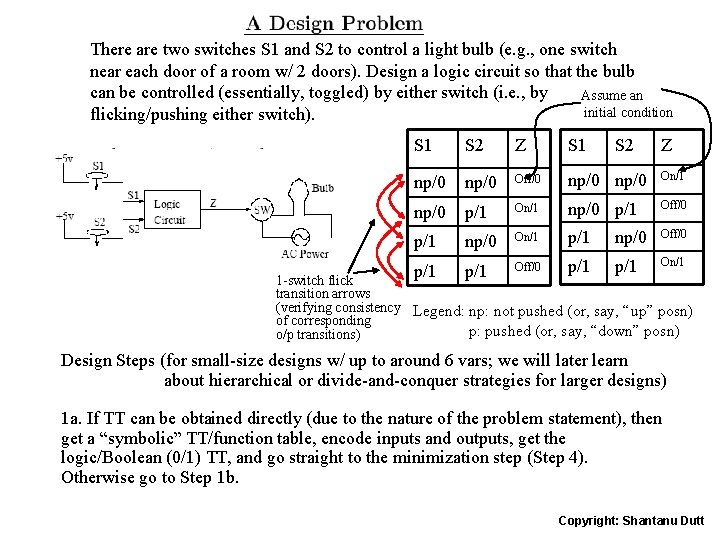
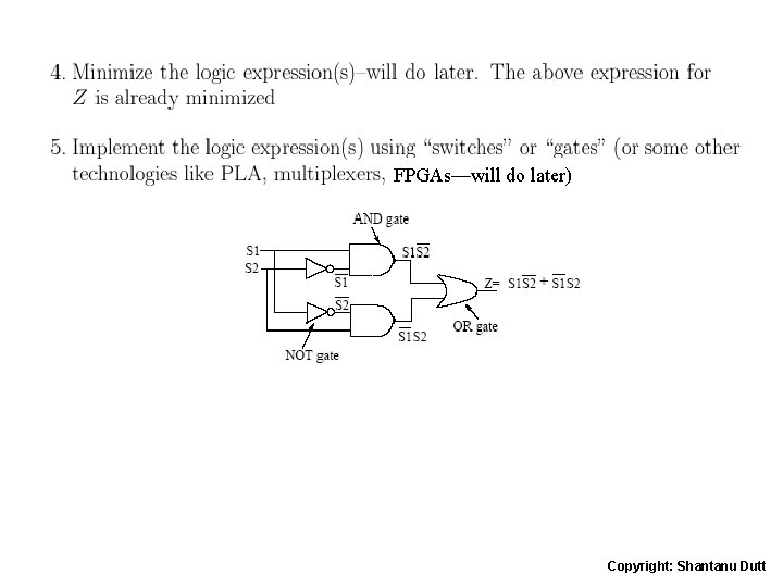
There are two switches S 1 and S 2 to control a light bulb (e. g. , one switch near each door of a room w/ 2 doors). Design a logic circuit so that the bulb can be controlled (essentially, toggled) by either switch (i. e. , by Assume an initial condition flicking/pushing either switch). S 1 S 2 Z np/0 Off/0 np/0 On/1 np/0 p/1 Off/0 p/1 np/0 On/1 p/1 np/0 Off/0 p/1 p/1 On/1 1 -switch flick transition arrows (verifying consistency Legend: np: not pushed (or, say, “up” posn) of corresponding p: pushed (or, say, “down” posn) o/p transitions) Design Steps (for small-size designs w/ up to around 6 vars; we will later learn about hierarchical or divide-and-conquer strategies for larger designs) 1 a. If TT can be obtained directly (due to the nature of the problem statement), then get a “symbolic” TT/function table, encode inputs and outputs, get the logic/Boolean (0/1) TT, and go straight to the minimization step (Step 4). Otherwise go to Step 1 b. Copyright: Shantanu Dutt

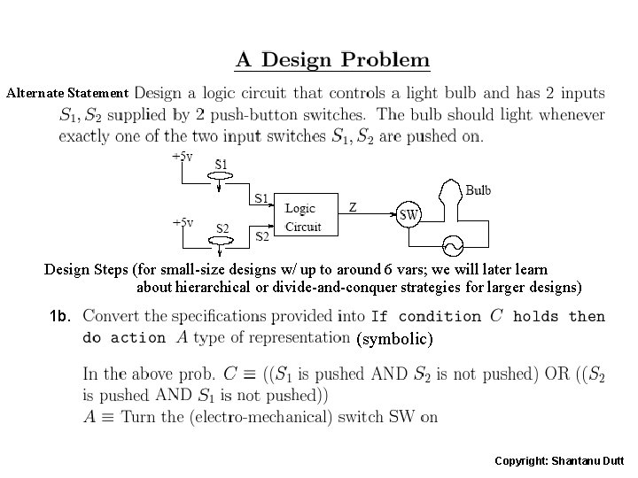
Alternate Statement Design Steps (for small-size designs w/ up to around 6 vars; we will later learn about hierarchical or divide-and-conquer strategies for larger designs) 1 b. (symbolic) Copyright: Shantanu Dutt

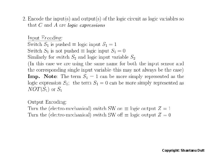
Copyright: Shantanu Dutt

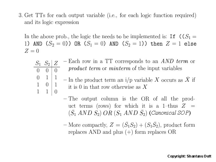
(Canonical SOP) Copyright: Shantanu Dutt

FPGAs—will do later) Copyright: Shantanu Dutt

Copyright: Shantanu Dutt

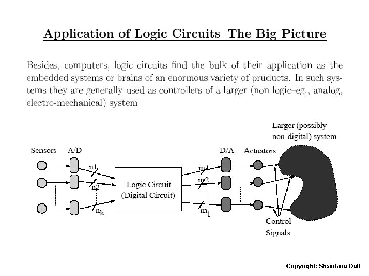
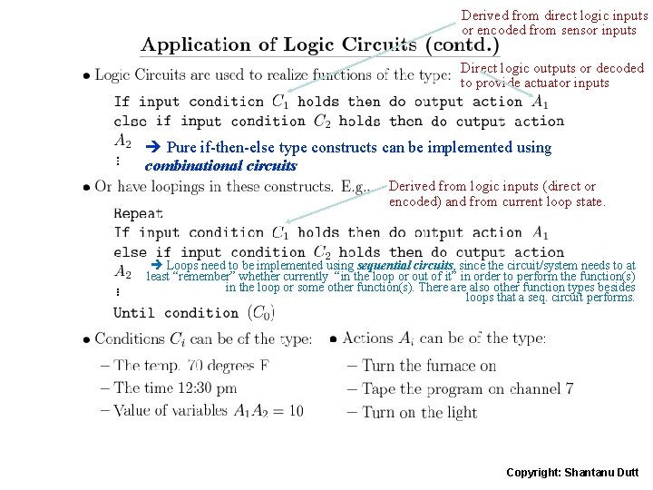
Derived from direct logic inputs or encoded from sensor inputs Direct logic outputs or decoded to provide actuator inputs Pure if-then-else type constructs can be implemented using combinational circuits Derived from logic inputs (direct or encoded) and from current loop state. Loops need to be implemented using sequential circuits, since the circuit/system needs to at least “remember” whether currently “in the loop or out of it” in order to perform the function(s) in the loop or some other function(s). There also other function types besides loops that a seq. circuit performs. Copyright: Shantanu Dutt

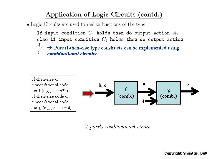
Pure if-then-else type constructs can be implemented using combinational circuits if-then-else or x unconditional codeneed to be implemented b, c using sequentialacircuits, since the circuit/system Loops f to re-do in each iteration g of the loop in needs at least “remember” what it needs for f (e. g. , a = to b*c) ordercode to perform the combinational function(s) in the loop. There also other if-then-else or besides (comb. ) function types loops that a seq. circuit performs. unconditional code d for g (e. g. , x = a + d) A purely combinational circuit Copyright: Shantanu Dutt

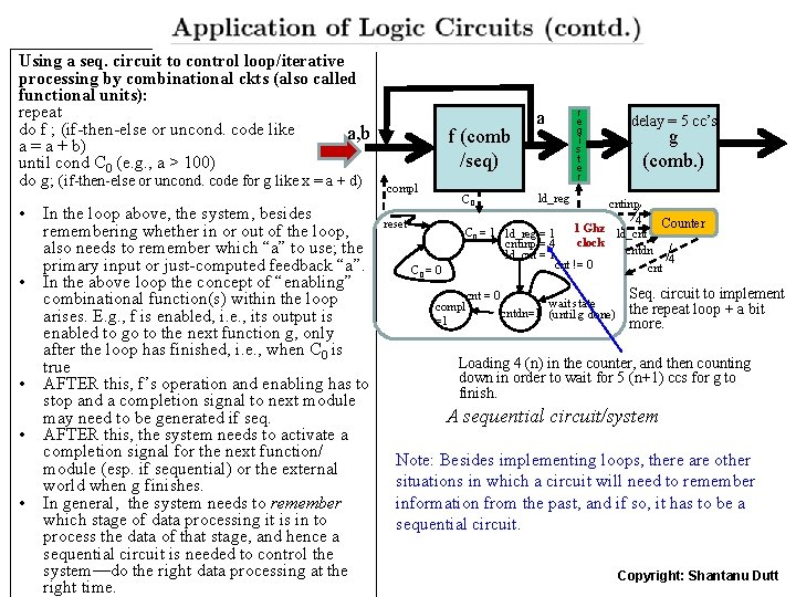
Using a seq. circuit to control loop/iterative processing by combinational ckts (also called functional units): repeat do f ; (if-then-else or uncond. code like a, b a = a + b) until cond C 0 (e. g. , a > 100) do g; (if-then-else or uncond. code for g like x = a + d) • • • In the loop above, the system, besides remembering whether in or out of the loop, also needs to remember which “a” to use; the primary input or just-computed feedback “a”. In the above loop the concept of “enabling” combinational function(s) within the loop arises. E. g. , f is enabled, i. e. , its output is enabled to go to the next function g, only after the loop has finished, i. e. , when C 0 is true AFTER this, f’s operation and enabling has to stop and a completion signal to next module may need to be generated if seq. AFTER this, the system needs to activate a completion signal for the next function/ module (esp. if sequential) or the external world when g finishes. In general, the system needs to remember which stage of data processing it is in to process the data of that stage, and hence a sequential circuit is needed to control the system—do the right data processing at the right time. f (comb /seq) compl C 0 reset C 0 = 0 a r e g i s t e r delay = 5 cc’s g (comb. ) ld_reg cntinp 4 Counter C 0 = 1 ld_reg = 1 1 Ghz ld_cnt clock cntinp = 4 cntdn ld_cnt = 1 4 cnt != 0 cnt compl =1 cnt = 0 wait state cntdn=1 (until g done) Seq. circuit to implement the repeat loop + a bit more. Loading 4 (n) in the counter, and then counting down in order to wait for 5 (n+1) ccs for g to finish. A sequential circuit/system Note: Besides implementing loops, there are other situations in which a circuit will need to remember information from the past, and if so, it has to be a sequential circuit. Copyright: Shantanu Dutt

Copyright: Shantanu Dutt

Copyright: Shantanu Dutt

Copyright: Shantanu Dutt

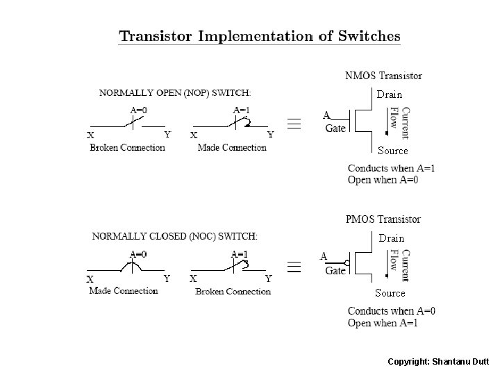
Drain Source Copyright: Shantanu Dutt

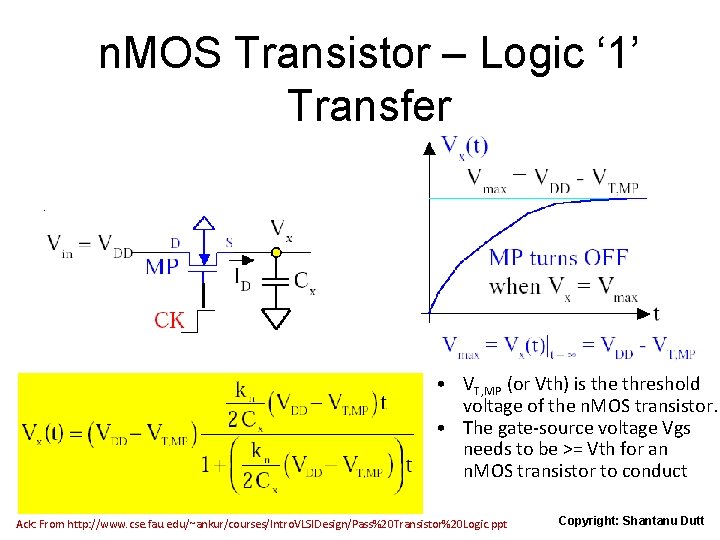
n. MOS Transistor – Logic ‘ 1’ Transfer • VT, MP (or Vth) is the threshold voltage of the n. MOS transistor. • The gate-source voltage Vgs needs to be >= Vth for an n. MOS transistor to conduct Ack: From http: //www. cse. fau. edu/~ankur/courses/Intro. VLSIDesign/Pass%20 Transistor%20 Logic. ppt Copyright: Shantanu Dutt

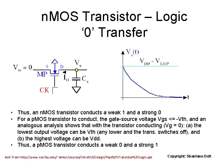
n. MOS Transistor – Logic ‘ 0’ Transfer • Thus, an n. MOS transistor conducts a weak 1 and a strong 0 • For a p. MOS transistor to conduct, the gate-source voltage Vgs <= -Vth, and an analogous analysis shows that with the transistor conducting (Vg = 0): (a) the lowest output voltage can be Vth (any lower and the trans. switches off), and (b) the highest voltage can be Vdd. • Thus, a p. MOS transistor conducts a weak 0 and a strong 1 Ack: From http: //www. cse. fau. edu/~ankur/courses/Intro. VLSIDesign/Pass%20 Transistor%20 Logic. ppt Copyright: Shantanu Dutt

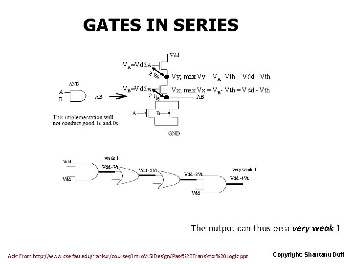
GATES IN SERIES VA=Vdd ≥V th VB=Vdd ≥V th Vdd Vy; max Vy = VA- Vth = Vdd - Vth Vx; max Vx = VB- Vth = Vdd - Vth weak 1 Vdd -Vt Vdd -2 Vt Vdd -3 Vt very weak 1 Vdd -4 Vt Vdd The output can thus be a very weak 1 Ack: From http: //www. cse. fau. edu/~ankur/courses/Intro. VLSIDesign/Pass%20 Transistor%20 Logic. ppt Copyright: Shantanu Dutt

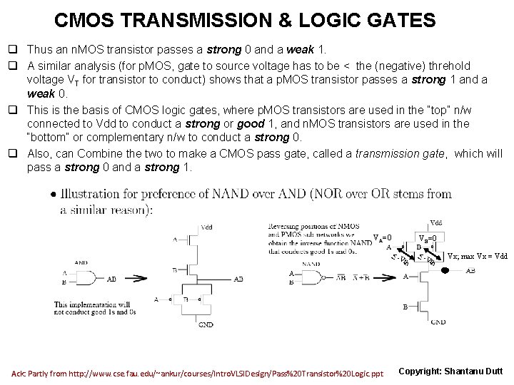
CMOS TRANSMISSION & LOGIC GATES q Thus an n. MOS transistor passes a strong 0 and a weak 1. q A similar analysis (for p. MOS, gate to source voltage has to be < the (negative) threhold voltage VT for transistor to conduct) shows that a p. MOS transistor passes a strong 1 and a weak 0. q This is the basis of CMOS logic gates, where p. MOS transistors are used in the “top” n/w connected to Vdd to conduct a strong or good 1, and n. MOS transistors are used in the “bottom” or complementary n/w to conduct a strong 0. q Also, can Combine the two to make a CMOS pass gate, called a transmission gate, which will pass a strong 0 and a strong 1. VA=0 VB=0 ≤- Vt Ack: Partly from http: //www. cse. fau. edu/~ankur/courses/Intro. VLSIDesign/Pass%20 Transistor%20 Logic. ppt h ≤- Vt h Vx; max Vx = Vdd Copyright: Shantanu Dutt

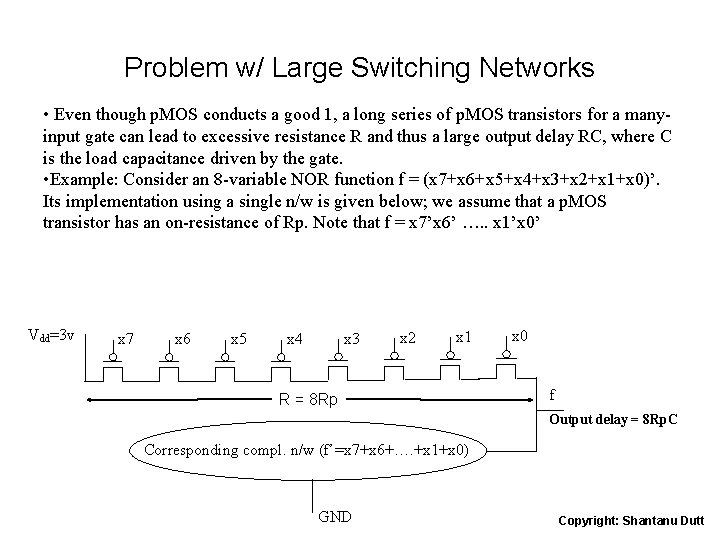
Problem w/ Large Switching Networks • Even though p. MOS conducts a good 1, a long series of p. MOS transistors for a manyinput gate can lead to excessive resistance R and thus a large output delay RC, where C is the load capacitance driven by the gate. • Example: Consider an 8 -variable NOR function f = (x 7+x 6+x 5+x 4+x 3+x 2+x 1+x 0)’. Its implementation using a single n/w is given below; we assume that a p. MOS transistor has an on-resistance of Rp. Note that f = x 7’x 6’ …. . x 1’x 0’ Vdd=3 v x 7 x 6 x 5 x 3 x 4 x 2 x 1 R = 8 Rp x 0 f Output delay = 8 Rp. C Corresponding compl. n/w (f’=x 7+x 6+…. +x 1+x 0) GND Copyright: Shantanu Dutt

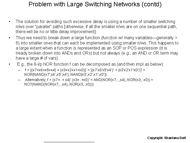
Problem with Large Switching Networks (contd) • • • The solution for avoiding such excessive delay is using a number of smaller switching n/ws over “parallel” paths [otherwise, if all the smaller n/ws are on one sequential path, there will be no or little delay improvement]. Thus we need to break down a large function (function w/ many variables—generally > 6) into smaller ones that can each be implemented using smaller n/ws. This happens to a large extent when a function is represented as an SOP or POS expression (it is lready broken down into ANDs and ORs) but not always (e. g. , an AND or OR term may have a large # of vars). E. g. , the 8 -i/p NOR function f can be decomposed as (and then impl as below): – – f = [(x 7+x 6+x 5+x 4) + (x 3+x 2+x 1+x 0)]’ = [(x 7’x 6’x 5’x 4’)’ + (x 3’x 2’x 1’x 0’)’]’ = NOR(NAND(x 7’, x 6’, x 5’, x 4’), NAND(x 3’, x 2’, x 1’, x 0’)). Alternatively, f = (x 7+. . + x 4)’ (x 3+. . +x 0)’ = AND(NOR(x 7, . . , x 4), NOR(x 3, . . x 0)) = NOT(NAND(NOR(x 7, . . , x 4), NOR(x 3, . . x 0))) Copyright: Shantanu Dutt

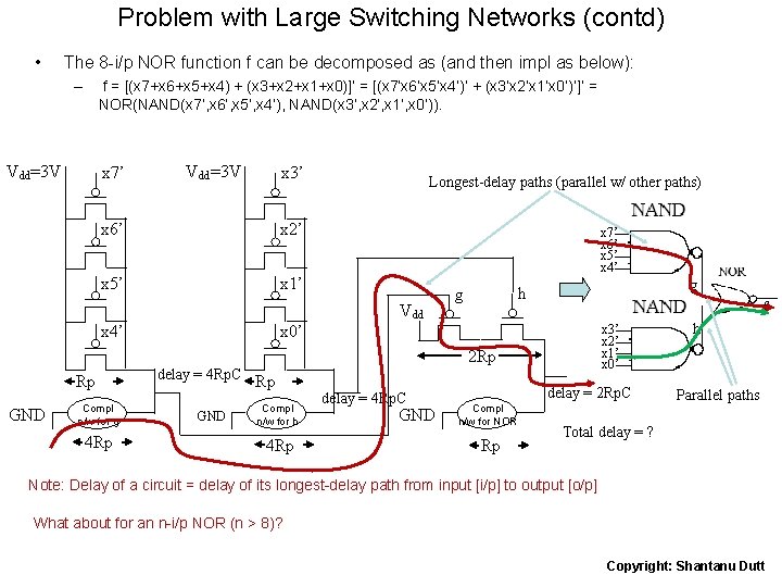
Problem with Large Switching Networks (contd) • The 8 -i/p NOR function f can be decomposed as (and then impl as below): – f = [(x 7+x 6+x 5+x 4) + (x 3+x 2+x 1+x 0)]’ = [(x 7’x 6’x 5’x 4’)’ + (x 3’x 2’x 1’x 0’)’]’ = NOR(NAND(x 7’, x 6’, x 5’, x 4’), NAND(x 3’, x 2’, x 1’, x 0’)). Vdd=3 V x 7’ Vdd=3 V x 3’ x 6’ x 2’ x 5’ x 1’ Longest-delay paths (parallel w/ other paths) x 7’ x 6’ x 5’ x 4’ Vdd x 4’ Rp GND Compl n/w for g 4 Rp g h g f x 0’ delay = 4 Rp. C GND x 3’ x 2’ x 1’ x 0’ 2 Rp Rp Compl n/w for h 4 Rp delay = 4 Rp. C GND delay = 2 Rp. C Compl n/w for NOR Rp h Parallel paths Total delay = ? Note: Delay of a circuit = delay of its longest-delay path from input [i/p] to output [o/p] What about for an n-i/p NOR (n > 8)? Copyright: Shantanu Dutt

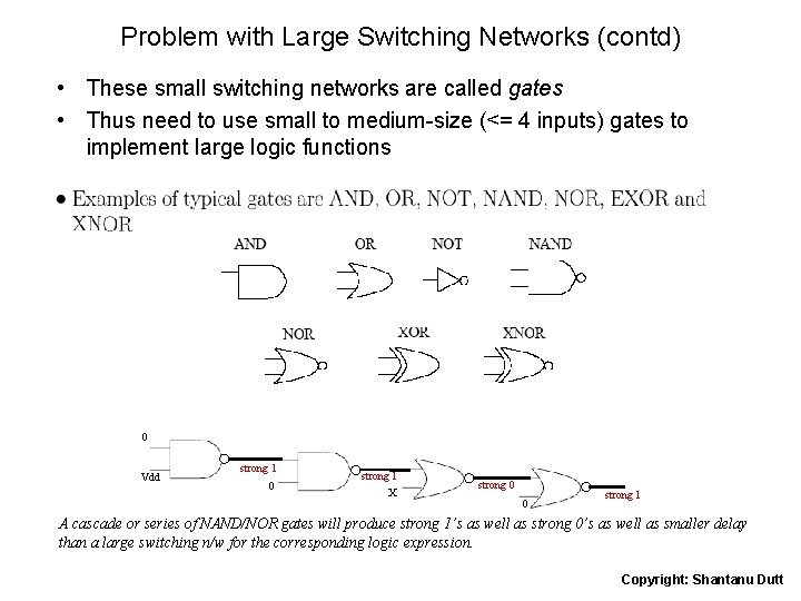
Problem with Large Switching Networks (contd) • These small switching networks are called gates • Thus need to use small to medium-size (<= 4 inputs) gates to implement large logic functions 0 Vdd strong 1 0 strong 1 X strong 0 0 strong 1 A cascade or series of NAND/NOR gates will produce strong 1’s as well as strong 0’s as well as smaller delay than a large switching n/w for the corresponding logic expression. Copyright: Shantanu Dutt

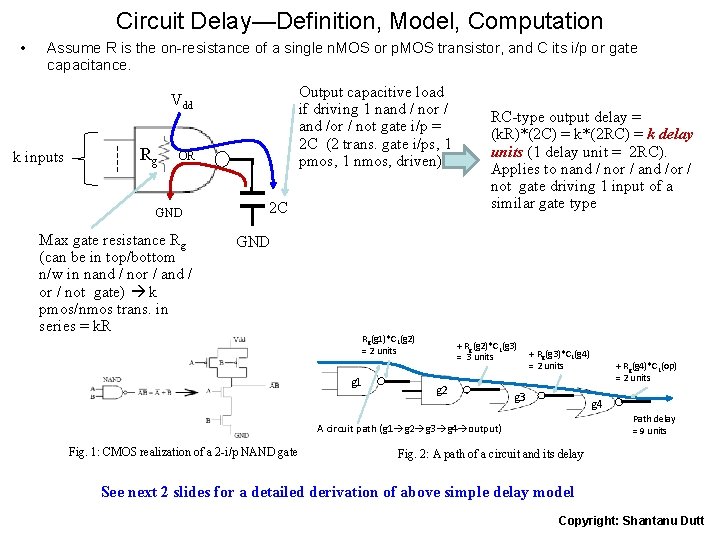
Circuit Delay—Definition, Model, Computation • Assume R is the on-resistance of a single n. MOS or p. MOS transistor, and C its i/p or gate capacitance. Output capacitive load if driving 1 nand / nor / and /or / not gate i/p = 2 C (2 trans. gate i/ps, 1 pmos, 1 nmos, driven) Vdd k inputs Rg OR GND Max gate resistance Rg (can be in top/bottom n/w in nand / nor / and / or / not gate) k pmos/nmos trans. in series = k. R 2 C RC-type output delay = (k. R)*(2 C) = k*(2 RC) = k delay units (1 delay unit = 2 RC). Applies to nand / nor / and /or / not gate driving 1 input of a similar gate type GND Rg(g 1)*CL(g 2) = 2 units g 1 + Rg(g 2)*CL(g 3) = 3 units g 2 + Rg(g 3)*CL(g 4) = 2 units g 3 g 4 Path delay = 9 units A circuit path (g 1 g 2 g 3 g 4 output) Fig. 1: CMOS realization of a 2 -i/p NAND gate + Rg(g 4)*CL(op) = 2 units Fig. 2: A path of a circuit and its delay See next 2 slides for a detailed derivation of above simple delay model Copyright: Shantanu Dutt

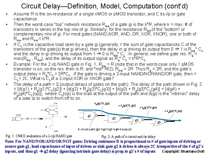
Circuit Delay—Definition, Model, Computation (cont’d) • • • Assume R is the on-resistance of a single n. MOS or p. MOS transistor, and C its i/p or gate capacitance. Then the worst-case “top” network resistance Rtop of a gate gi is the k*R, where k = max. # of transistors in series in the top n/w of gi. Similarly, for the resistance Rbot of the “bottom” or complementary n/w of gi. For most gates (NAND, NOR, AND, OR, XNOR), one or both of Rtop and Rbot = k*R. If CL is the capacitive load seen by a gate gi (generally = the sum of gate capacitances C of the transistors of the gate(s) that gi drives), then the delay in gi driving its output from 0 1 is Rtop* CL and the delay in gi driving its output from 1 0 is Rbot* CL. In general, we define gate res. Rg = max(Rtop , Rbot), and the delay of its output signal as Rg* CL = k*R*CL Example: For the 2 i/p NAND gate in Fig. 1, Rtop = R (note that in the worst-case only 1 p. MOS transistor is on, so the res. then is R, and *not* R/2), Rbot = 2 R. Thus Rg = 2 R, and the gate’s output delay = Rg*CL = 2 R*CL. If the gate is driving a 2 -input NAND/NOR/AND/OR gate, then = CL= 2 C. What is CLof a 2 -input XOR or XNOR gate? The delay of a path = S (output delays of gates on the path). The delay of the path shown in Fig. 2 = [d(g 1) + Rg(g 1)*CL(g 2)] + [d(g 2) + Rg(g 2)*CL(g 3)] + [d(g 3) + Rg(g 3)*CL(g 4)] + [d(g 4) + Rg(g 4)*CL(op)], where CL(op) is the load at the output of the path and d(gi) is the “intrinsic” delay of a gate gi to switch from off to on. Rg(g 1)*CL(g 2) g 1 + Rg(g 2)*CL(g 3) g 2 + Rg(g 3)*CL(g 4) g 3 + Rg(g 4)*CL(op) g 4 A circuit path (g 1 g 2 g 3 g 4 output) Fig. 1: CMOS realization of a 2 -i/p NAND gate Fig. 2: A path of a circuit and its delay Note: For NAND/NOR/AND/OR/NOT gates: Driving resistance R is proportional to # of gate inputs of driving or source gate g 1, load capacitance of input of driven or sink gate g 2 it drives is always 2 C irrespective of the # of g 2’s inputs, and thus g 1 g 2 delay (ignoring intrinsic gate delay) is prop. to g 1’s # of inputs Copyright: Shantanu Dutt

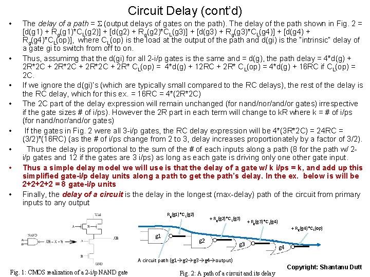
Circuit Delay (cont’d) • • The delay of a path = S (output delays of gates on the path). The delay of the path shown in Fig. 2 = [d(g 1) + Rg(g 1)*CL(g 2)] + [d(g 2) + Rg(g 2)*CL(g 3)] + [d(g 3) + Rg(g 3)*CL(g 4)] + [d(g 4) + Rg(g 4)*CL(op)], where CL(op) is the load at the output of the path and d(gi) is the “intrinsic” delay of a gate gi to switch from off to on. Thus, assumimg that the d(gi) for all 2 -i/p gates is the same and = d(g), the path delay = 4*d(g) + 2 R*2 C + 2 R* CL(op) = 4*d(g) + 12 RC + 2 R* CL(op) = 4*d(g) + 16 RC if CL(op) = 2 C. If we ignore the d(gi)’s (which are typically small compared to the RC delays), the rest of the delay is the RC delay, which for this ex. = 16 RC = 4*(2 R*2 C) The 2 C part of the delay expression will remain unchanged (for nand/nor/and/or gates) irrespective if the gate sizes # of i/ps). However the 2 R part in each term will change to k. R where k = # of i/ps (for nand/nor/and/or gates) If the gates in Fig. 2 were all 3 -i/p gates, the RC delay expression will be 4*(3 R*2 C) = 24 RC = (3/2)*(16 RC) (as the # of i/ps change from 2 to 3, delay increases proportionately by a factor of 3/2). Thus the delay is proportional to the sum of the # of each inputs along a path (8 for the path w/ 2 i/p gates and 12 if the gates are 3 i/ps) as long as each gate is driving only one other gate input. Thus a simple delay model we will use is that the delay of a gate w/ k i/ps = k, and add up this simplified gate-i/p delay units along a path to get the path’s delay. In the ex. below is will be 2+2+2+2 = 8 gate-i/p units Finally, the delay of a circuit is the delay in the longest (max-delay) path of the circuit from primary inputs to any output Rg(g 1)*CL(g 2) g 1 + Rg(g 2)*CL(g 3) g 2 + Rg(g 3)*CL(g 4) g 3 + Rg(g 4)*CL(op) g 4 A circuit path (g 1 g 2 g 3 g 4 output) Fig. 1: CMOS realization of a 2 -i/p NAND gate Fig. 2: A path of a circuit and its delay Copyright: Shantanu Dutt

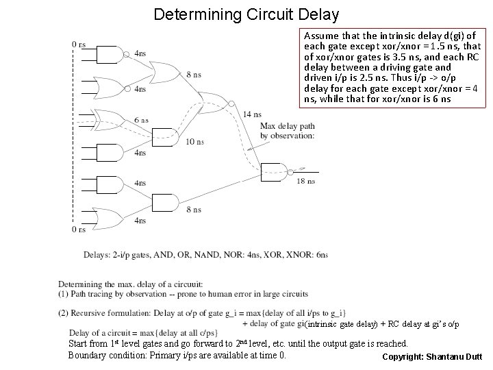
Determining Circuit Delay Assume that the intrinsic delay d(gi) of each gate except xor/xnor = 1. 5 ns, that of xor/xnor gates is 3. 5 ns, and each RC delay between a driving gate and driven i/p is 2. 5 ns. Thus i/p -> o/p delay for each gate except xor/xnor = 4 ns, while that for xor/xnor is 6 ns (intrinsic gate delay) + RC delay at gi’s o/p Start from 1 st level gates and go forward to 2 nd level, etc. until the output gate is reached. Boundary condition: Primary i/ps are available at time 0. Copyright: Shantanu Dutt