EECS 465 Digital Systems Design Lecture Notes Logic

- Slides: 26

EECS 465: Digital Systems Design Lecture Notes Logic Design Using Compound Components: Multiplexers SHANTANU DUTT Department of Electrical and Computer Science University of Illinois, Chicago Phone: (312) 355 -1314; e-mail: dutt@eecs. uic. edu URL: http: //www. eecs. uic. edu/~dutt 1

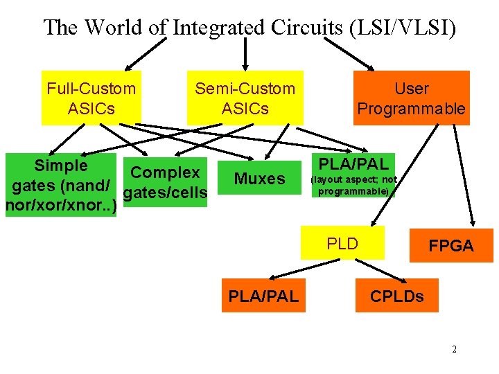
The World of Integrated Circuits (LSI/VLSI) Full-Custom ASICs Semi-Custom ASICs Simple Complex gates (nand/ gates/cells nor/xnor. . ) Muxes User Programmable PLA/PAL (layout aspect; not programmable) PLD PLA/PAL FPGA CPLDs 2

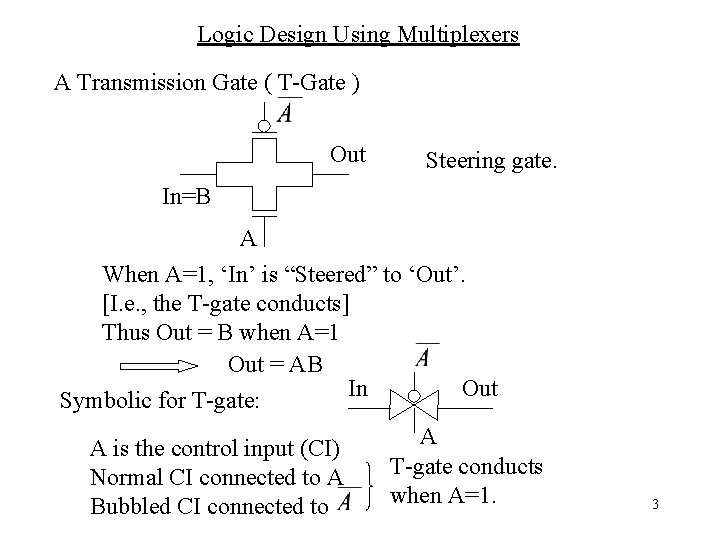
Logic Design Using Multiplexers A Transmission Gate ( T-Gate ) Out Steering gate. In=B A When A=1, ‘In’ is “Steered” to ‘Out’. [I. e. , the T-gate conducts] Thus Out = B when A=1 Out = AB In Out Symbolic for T-gate: A A is the control input (CI) T-gate conducts Normal CI connected to A when A=1. Bubbled CI connected to 3

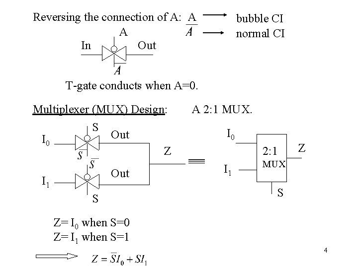
Reversing the connection of A: A A In Out bubble CI normal CI T-gate conducts when A=0. Multiplexer (MUX) Design: S Out I 0 Z Out I 1 S A 2: 1 MUX. I 0 2: 1 I 1 Z MUX S Z= I 0 when S=0 Z= I 1 when S=1 4

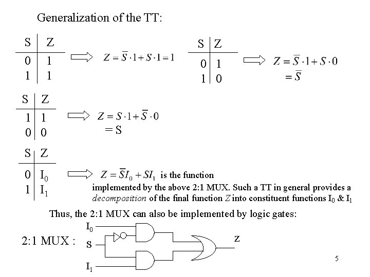
Generalization of the TT: S 0 1 Z 1 1 S Z 0 1 1 0 S Z 1 1 0 0 =S S Z 0 I 0 1 I 1 is the function implemented by the above 2: 1 MUX. Such a TT in general provides a decomposition of the final function Z into constituent functions I 0 & I 1 Thus, the 2: 1 MUX can also be implemented by logic gates: I 0 2: 1 MUX : S I 1 z 5

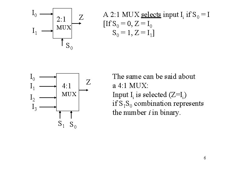
I 0 I 1 2: 1 A 2: 1 MUX selects input Ii if S 0 = I [If S 0 = 0, Z = I 0 S 0 = 1, Z = I 1] Z MUX S 0 I 1 I 2 I 3 4: 1 MUX Z The same can be said about a 4: 1 MUX: Input Ii is selected (Z=Ii) if S 1 S 0 combination represents the number i in binary. S 1 S 0 6

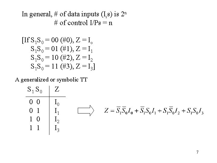
In general, # of data inputs (Iis) is 2 n # of control I/Ps = n [If S 1 S 0 = 00 (#0), Z = Io S 1 S 0 = 01 (#1), Z = I 1 S 1 S 0 = 10 (#2), Z = I 2 S 1 S 0 = 11 (#3), Z = I 3] A generalized or symbolic TT S 1 S 0 Z 0 0 1 1 I 0 I 1 I 2 I 3 0 1 7

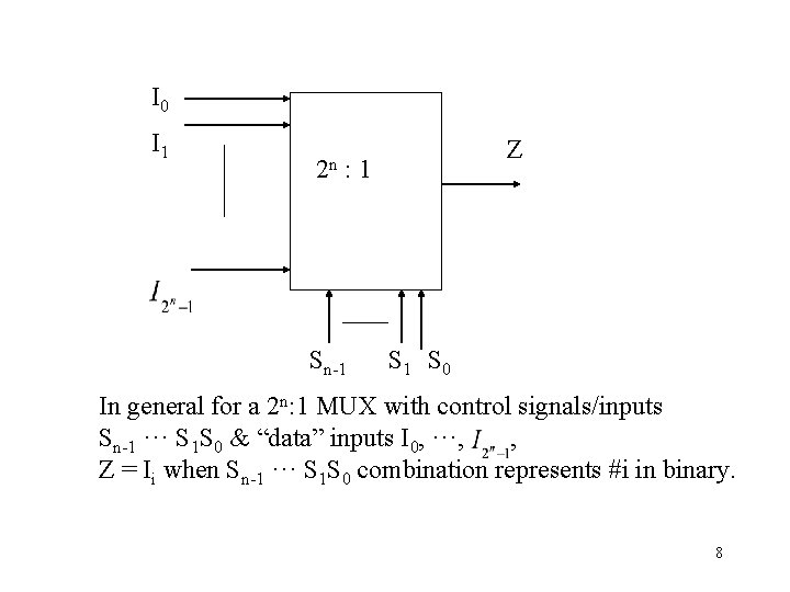
I 0 I 1 2 n Z : 1 Sn-1 S 0 In general for a 2 n: 1 MUX with control signals/inputs Sn-1 ··· S 1 S 0 & “data” inputs I 0, ···, , Z = Ii when Sn-1 ··· S 1 S 0 combination represents #i in binary. 8

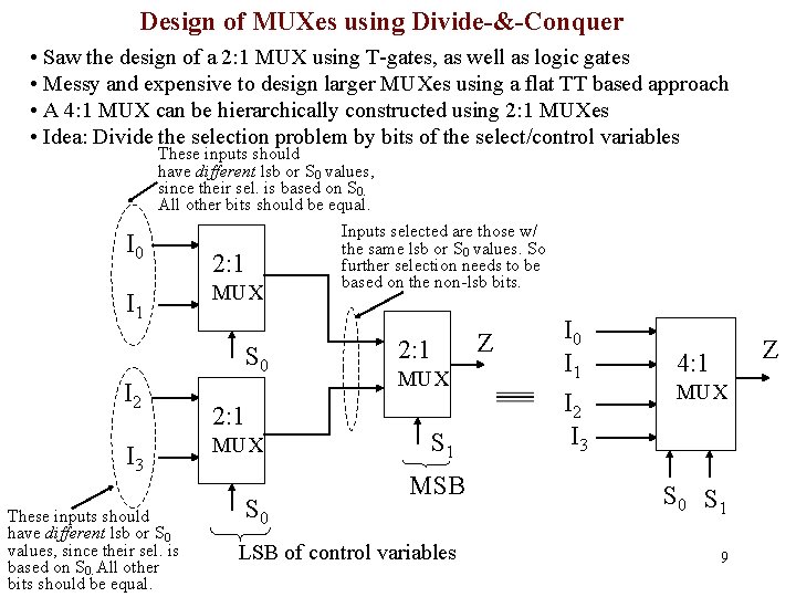
Design of MUXes using Divide-&-Conquer • Saw the design of a 2: 1 MUX using T-gates, as well as logic gates • Messy and expensive to design larger MUXes using a flat TT based approach • A 4: 1 MUX can be hierarchically constructed using 2: 1 MUXes • Idea: Divide the selection problem by bits of the select/control variables These inputs should have different lsb or S 0 values, since their sel. is based on S 0. All other bits should be equal. I 0 I 1 2: 1 MUX S 0 I 2 I 3 These inputs should have different lsb or S 0 values, since their sel. is based on S 0. All other bits should be equal. 2: 1 MUX S 0 Inputs selected are those w/ the same lsb or S 0 values. So further selection needs to be based on the non-lsb bits. 2: 1 MUX S 1 MSB LSB of control variables Z I 0 I 1 I 2 I 3 Z 4: 1 MUX S 0 S 1 9

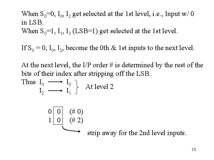
When S 0=0, I 2 get selected at the 1 st level, i. e. , Input w/ 0 in LSB. When S 0=1, I 3 (LSB=1) get selected at the 1 st level. If S 0 = 0, I 2, become the 0 th & 1 st inputs to the next level. At the next level, the I/P order # is determined by the rest of the bits of their index after stripping off the LSB. Thus I 0 At level 2 I 1 0 0 1 0 (# 0) (# 2) strip away for the 2 nd level inputs. 10

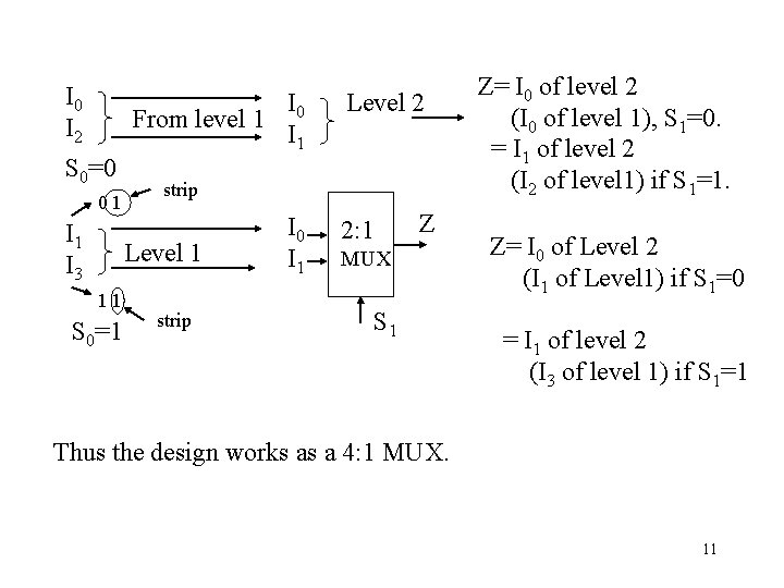
I 0 I 2 I 0 From level 1 I 1 S 0=0 01 I 3 strip Level 1 11 S 0=1 Level 2 strip I 0 I 1 2: 1 Z MUX S 1 Z= I 0 of level 2 (I 0 of level 1), S 1=0. = I 1 of level 2 (I 2 of level 1) if S 1=1. Z= I 0 of Level 2 (I 1 of Level 1) if S 1=0 = I 1 of level 2 (I 3 of level 1) if S 1=1 Thus the design works as a 4: 1 MUX. 11

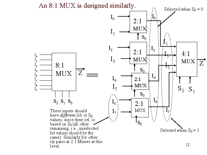
An 8: 1 MUX is designed similarly. I 0 I 1 I 2 I 3 I 4 I 5 I 6 I 7 8: 1 MUX Z I 3 These inputs should have different lsb or S 0 values, since their sel. is based on S 0 (all other remaining, i. e. , unselected bit values should be the same). Similarly for other i/p pairs at 2: 1 Muxes at this level. 2: 1 I 4 I 0 MUX S 0 2: 1 I 2 MUX S 0 I 5 S 2 S 1 S 0 Selected when S 0 = 0 2: 1 MUX S 0 I 6 2: 1 I 7 MUX I 1 I 3 I 5 4: 1 MUX I 4 S 2 S 1 I 6 I 7 S 0 Selected when S 0 = 1 12 Z

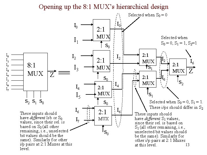
Opening up the 8: 1 MUX’s hierarchical design Selected when S 0 = 0 I 1 I 2 I 3 I 4 I 5 I 6 I 7 I 2 8: 1 MUX Z I 3 These inputs should have different lsb or S 0 values, since their sel. is based on S 0 (all other remaining, i. e. , unselected bit values should be the same). Similarly for other i/p pairs at 2: 1 Muxes at this level. MUX I 5 Selected when S 0 = 0, S 1 = 1, S 2=1 S 0 2: 1 I 2 MUX S 0 I 4 S 2 S 1 S 0 2: 1 I 0 2: 1 MUX I 4 2: 1 I 7 MUX S 0 I 2 2: 1 MUX I 6 Z S 2 S 1 S 0 I 6 2: 1 MUX S 1 I 6 Selected when S 0 = 0, S 1 = 1. These i/ps should differ in S 2 These inputs should have different S 1 values, since their sel. is based on S 1 (all other remaining, i. e. , unselected bit values should be the same). Similarly for other i/p pairs at 2: 1 Muxes 13 at this level.

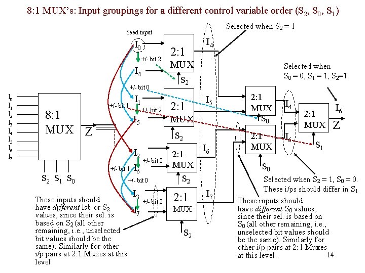
8: 1 MUX’s: Input groupings for a different control variable order (S 2, S 0, S 1) Selected when S 2 = 1 Seed input I 0 +/- bit 2 I 4 +/- bit 0 I 1 I 2 I 3 I 4 I 5 I 6 I 7 8: 1 MUX Z +/- bit 1 I 5 +/- bit 2 2: 1 I 4 MUX Selected when S 0 = 0, S 1 = 1, S 2=1 S 2 2: 1 I 5 MUX S 2 +/- bit 1 S 2 S 1 S 0 These inputs should have different lsb or S 2 values, since their sel. is based on S 2 (all other remaining, i. e. , unselected bit values should be the same). Similarly for other i/p pairs at 2: 1 Muxes at this level. I 6 I 2 2: 1 +/- bit 2 MUX I 6 +/- bit 0 I 3 I 7 +/- bit 2 S 2 2: 1 MUX S 2 I 7 2: 1 MUX S 0 I 4 2: 1 MUX I 6 Z S 1 S 0 Selected when S 2 = 1, S 0 = 0. These i/ps should differ in S 1 These inputs should have different S 0 values, since their sel. is based on S 0 (all other remaining, i. e. , unselected bit values should be the same). Similarly for other i/p pairs at 2: 1 Muxes 14 at this level.

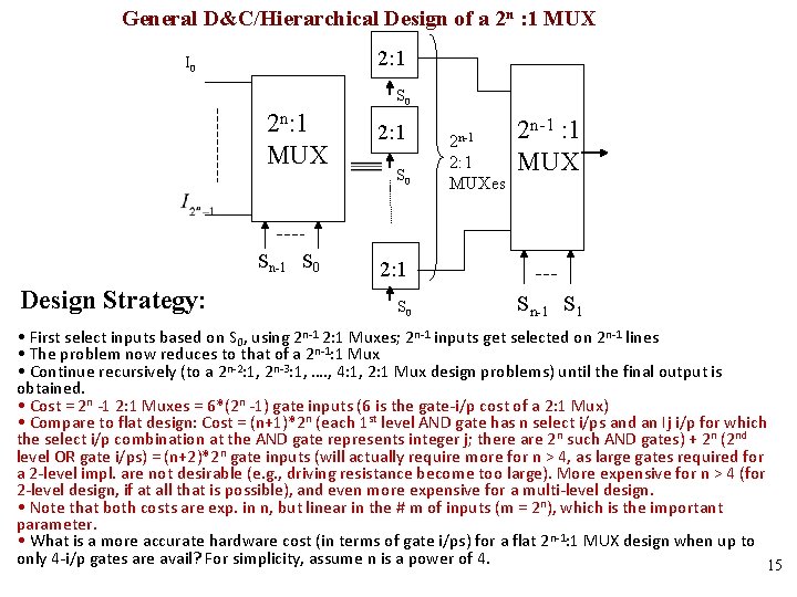
General D&C/Hierarchical Design of a 2 n : 1 MUX 2: 1 I 0 S 0 2 n: 1 MUX Sn-1 S 0 Design Strategy: 2: 1 S 0 2 n-1 2: 1 MUXes 2 n-1 : 1 MUX 2: 1 S 0 Sn-1 S 1 • First select inputs based on S 0, using 2 n-1 2: 1 Muxes; 2 n-1 inputs get selected on 2 n-1 lines • The problem now reduces to that of a 2 n-1: 1 Mux • Continue recursively (to a 2 n-2: 1, 2 n-3: 1, …. , 4: 1, 2: 1 Mux design problems) until the final output is obtained. • Cost = 2 n -1 2: 1 Muxes = 6*(2 n -1) gate inputs (6 is the gate-i/p cost of a 2: 1 Mux) • Compare to flat design: Cost = (n+1)*2 n (each 1 st level AND gate has n select i/ps and an Ij i/p for which the select i/p combination at the AND gate represents integer j; there are 2 n such AND gates) + 2 n (2 nd level OR gate i/ps) = (n+2)*2 n gate inputs (will actually require more for n > 4, as large gates required for a 2 -level impl. are not desirable (e. g. , driving resistance become too large). More expensive for n > 4 (for 2 -level design, if at all that is possible), and even more expensive for a multi-level design. • Note that both costs are exp. in n, but linear in the # m of inputs (m = 2 n), which is the important parameter. • What is a more accurate hardware cost (in terms of gate i/ps) for a flat 2 n-1: 1 MUX design when up to only 4 -i/p gates are avail? For simplicity, assume n is a power of 4. 15

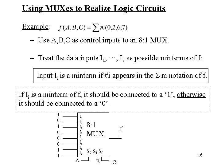
Using MUXes to Realize Logic Circuits Example: -- Use A, B, C as control inputs to an 8: 1 MUX. -- Treat the data inputs I 0, ···, I 7 as possible minterms of f: Input Ii is a minterm if #i appears in the m notation of f. If Ii is a minterm of f, it should be connected to a ‘ 1’, otherwise it should be connected to a ‘ 0’. 1 0 0 0 1 1 I 0 I 1 I 2 I 3 I 4 I 5 I 6 I 7 A 8: 1 MUX f S 2 S 1 S 0 B 16 C

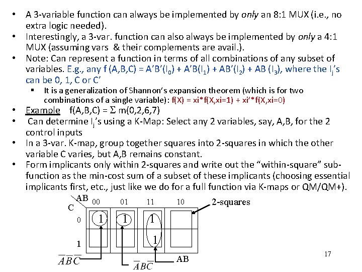
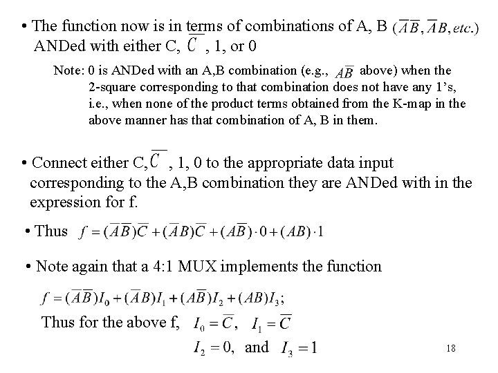
• A 3 -variable function can always be implemented by only an 8: 1 MUX (i. e. , no extra logic needed). • Interestingly, a 3 -var. function can also always be implemented by only a 4: 1 MUX (assuming vars & their complements are avail. ). • Note: Can represent a function in terms of all combinations of any subset of variables. E. g. , any f (A, B, C) = A’B’(I 0) + A’B(I 1) + AB’(I 2) + AB (I 3), where the Ij’s can be 0, 1, C or C’ § It is a generalization of Shannon’s expansion theorem (which is for two combinations of a single variable): f(X) = xi*f(X, xi=1) + xi’*f(X, xi=0) • Example f(A, B, C) = m(0, 2, 6, 7) • Can determine Ij’s using a K-Map: Select any 2 variables, say, A, B, for the 2 control inputs • In a 3 -var. K-map, group together squares into 2 -squares in which the other variable C varies, but A, B remains constant. • Form implicants only within 2 -squares and write out the “within-square” subfunction as the min-cost sum of a subset of these implicants (choosing essential implicants first, etc. , just like we do for a full function via K-maps or QM/QM+). AB 00 01 11 10 2 -squares C 0 1 1 1 AB 17

• The function now is in terms of combinations of A, B ANDed with either C, , 1, or 0 Note: 0 is ANDed with an A, B combination (e. g. , above) when the 2 -square corresponding to that combination does not have any 1’s, i. e. , when none of the product terms obtained from the K-map in the above manner has that combination of A, B in them. • Connect either C, , 1, 0 to the appropriate data input corresponding to the A, B combination they are ANDed with in the expression for f. • Thus • Note again that a 4: 1 MUX implements the function Thus for the above f, and 18

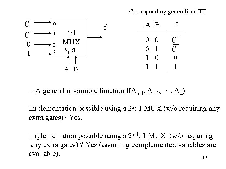
Corresponding generalized TT 0 1 2 3 4: 1 MUX S 1 S 0 A B f 0 0 1 1 0 1 0 1 -- A general n-variable function f(An-1, An-2, ···, A 0) Implementation possible using a 2 n: 1 MUX (w/o requiring any extra gates)? Yes. Implementation possible using a 2 n-1: 1 MUX (w/o requiring any extra gates) ? Yes (assuming complemented variables are available). 19

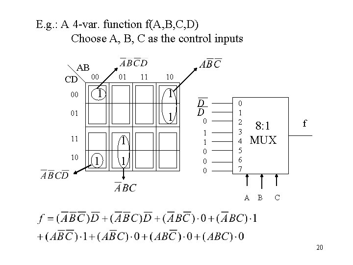
E. g. : A 4 -var. function f(A, B, C, D) Choose A, B, C as the control inputs AB CD 00 00 01 1 10 1 01 1 1 11 10 11 1 1 0 0 0 0 1 2 3 4 5 6 7 8: 1 MUX A B f C 20

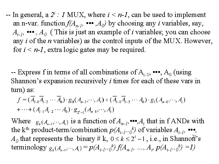
-- In general, a 2 i : 1 MUX, where i < n-1, can be used to implement an n-var. function f(An-1, • • • , A 0) by choosing any i variables, say, Ai-1, • • • , A 0 ( This is just an example of i variables; you can choose any i of the n variables) as the control inputs of the MUX. However, for i < n-1, extra logic gates may be required. -- Express f in terms of all combinations of Ai-1, • • • , A 0 (using Shannon’s expansion recursively i times for each of these vars in turn) as: Where is a function of An-1, • • • , Ai that in f ANDs with the kth product-term/combination p(Ai-1. . 0 k) of variables Ai-1, • • • , 21 A 0 that represents the binary # k, , i. e. , in Shannon’s terminology = p(Ai-1. . 0 k) f(An-1, …, Ai, p(Ai-1. . 0 k) =1)

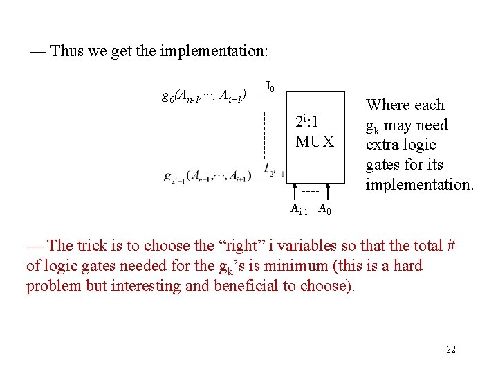
— Thus we get the implementation: g 0(An-1, ···, Ai+1) I 0 2 i: 1 MUX Where each gk may need extra logic gates for its implementation. Ai-1 A 0 — The trick is to choose the “right” i variables so that the total # of logic gates needed for the gk’s is minimum (this is a hard problem but interesting and beneficial to choose). 22

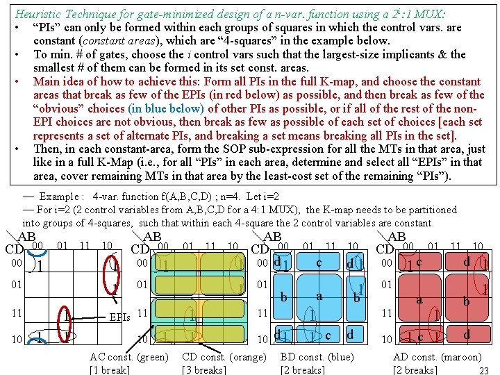
Heuristic Technique for gate-minimized design of a n-var. function using a 2 i: 1 MUX: • “PIs” can only be formed within each groups of squares in which the control vars. are constant (constant areas), which are “ 4 -squares” in the example below. • To min. # of gates, choose the i control vars such that the largest-size implicants & the smallest # of them can be formed in its set const. areas. • Main idea of how to achieve this: Form all PIs in the full K-map, and choose the constant areas that break as few of the EPIs (in red below) as possible, and then break as few of the “obvious” choices (in blue below) of other PIs as possible, or if all of the rest of the non. EPI choices are not obvious, then break as few as possible of each set of choices [each set represents a set of alternate PIs, and breaking a set means breaking all PIs in the set]. • Then, in each constant-area, form the SOP sub-expression for all the MTs in that area, just like in a full K-Map (i. e. , for all “PIs” in each area, determine and select all “EPIs” in that area, cover remaining MTs in that area by the least-cost set of the remaining “PIs”). — Example : 4 -var. function f(A, B, C, D) ; n=4. Let i=2 — For i=2 (2 control variables from A, B, C, D for a 4: 1 MUX), the K-map needs to be partitioned into groups of 4 -squares, such that within each 4 -square the 2 control variables are constant. AB CD 00 00 01 10 1 1 01 1 11 10 11 1 AB CD 00 00 01 10 1 1 01 1 EPIs 11 10 11 1 AC const. (green) [1 break] 1 1 AB CD 00 00 d 1 01 b 11 10 CD const. (orange) [3 breaks] d 1 01 11 10 c d 1 a b 1 1 1 c d BD const. (blue) [2 breaks] AB CD 00 00 01 11 10 1 c d a b 01 11 10 1 1 c 1 1 1 d AD const. (maroon) [2 breaks] 23

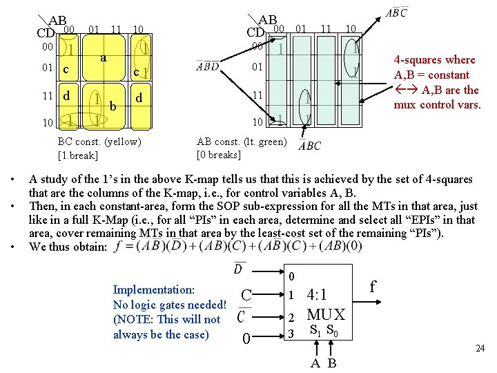
AB CD 00 00 1 01 c 11 d 10 1 01 11 10 1 a 1 b 1 • • 00 c 1 01 d 11 BC const. (yellow) [1 break] • AB CD 00 10 01 11 10 1 1 4 -squares where A, B = constant A, B are the mux control vars. 1 1 AB const. (lt. green) [0 breaks] A study of the 1’s in the above K-map tells us that this is achieved by the set of 4 -squares that are the columns of the K-map, i. e. , for control variables A, B. Then, in each constant-area, form the SOP sub-expression for all the MTs in that area, just like in a full K-Map (i. e. , for all “PIs” in each area, determine and select all “EPIs” in that area, cover remaining MTs in that area by the least-cost set of the remaining “PIs”). We thus obtain: Implementation: No logic gates needed! (NOTE: This will not always be the case) 0 C 0 1 2 3 4: 1 MUX f S 1 S 0 24 A B

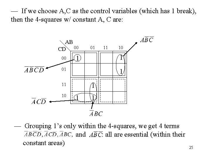
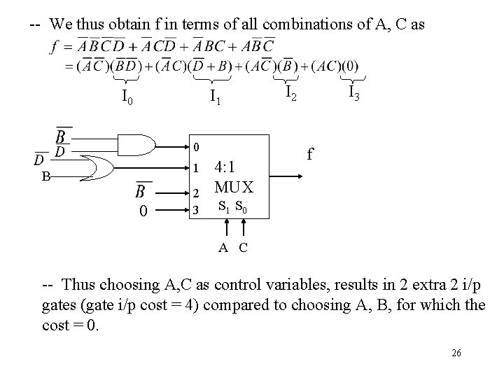
— If we choose A, C as the control variables (which has 1 break), then the 4 -squares w/ constant A, C are: AB CD 00 00 01 10 1 1 01 1 1 11 10 11 1 1 — Grouping 1’s only within the 4 -squares, we get 4 terms and : all are essential (within their constant areas) 25

-- We thus obtain f in terms of all combinations of A, C as I 0 I 1 0 1 B 0 2 3 4: 1 MUX I 2 I 3 f S 1 S 0 A C -- Thus choosing A, C as control variables, results in 2 extra 2 i/p gates (gate i/p cost = 4) compared to choosing A, B, for which the cost = 0. 26