ECE 465 High Level Design Strategies Lecture Notes

- Slides: 53

ECE 465 High Level Design Strategies Lecture Notes # 9 Shantanu Dutt Electrical & Computer Engineering University of Illinois at Chicago

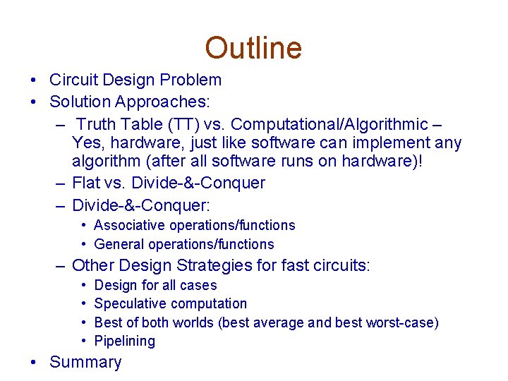
Outline • Circuit Design Problem • Solution Approaches: – Truth Table (TT) vs. Computational/Algorithmic – Yes, hardware, just like software can implement any algorithm (after all software runs on hardware)! – Flat vs. Divide-&-Conquer – Divide-&-Conquer: • Associative operations/functions • General operations/functions – Other Design Strategies for fast circuits: • • Design for all cases Speculative computation Best of both worlds (best average and best worst-case) Pipelining • Summary

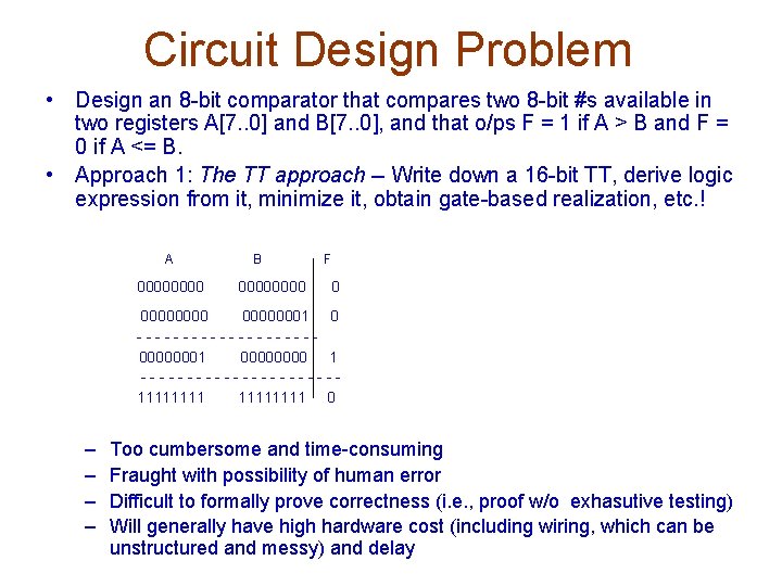
Circuit Design Problem • Design an 8 -bit comparator that compares two 8 -bit #s available in two registers A[7. . 0] and B[7. . 0], and that o/ps F = 1 if A > B and F = 0 if A <= B. • Approach 1: The TT approach -- Write down a 16 -bit TT, derive logic expression from it, minimize it, obtain gate-based realization, etc. ! A 0000 B 0000 F 0 00000001 0 ----------00000001 0000 1 -----------11111111 0 – – Too cumbersome and time-consuming Fraught with possibility of human error Difficult to formally prove correctness (i. e. , proof w/o exhasutive testing) Will generally have high hardware cost (including wiring, which can be unstructured and messy) and delay

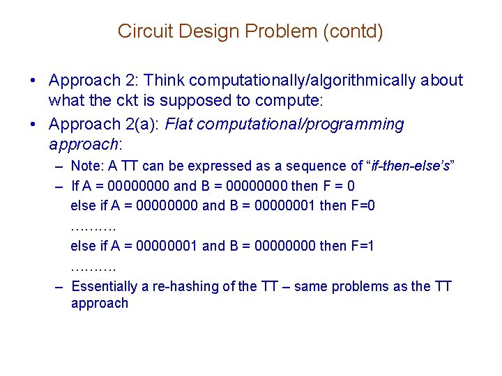
Circuit Design Problem (contd) • Approach 2: Think computationally/algorithmically about what the ckt is supposed to compute: • Approach 2(a): Flat computational/programming approach: – Note: A TT can be expressed as a sequence of “if-then-else’s” – If A = 0000 and B = 0000 then F = 0 else if A = 0000 and B = 00000001 then F=0 ………. else if A = 00000001 and B = 0000 then F=1 ………. – Essentially a re-hashing of the TT – same problems as the TT approach

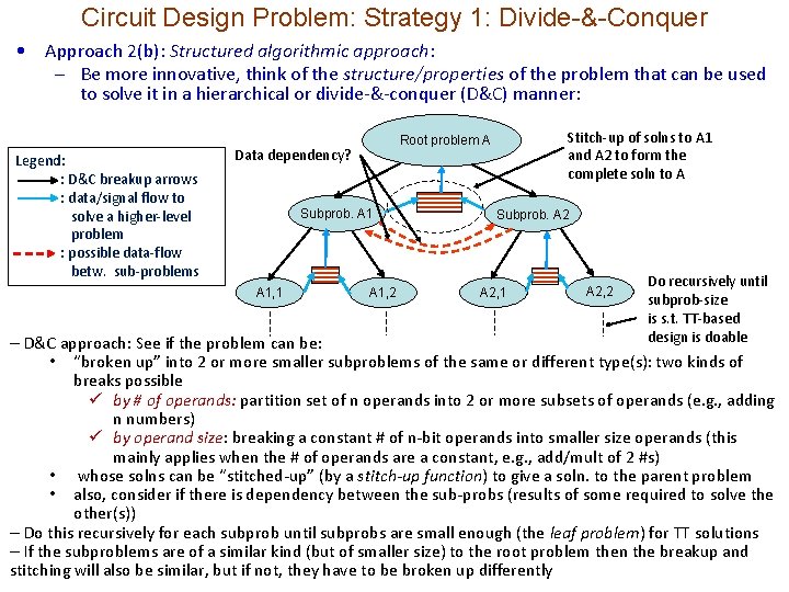
Circuit Design Problem: Strategy 1: Divide-&-Conquer • Approach 2(b): Structured algorithmic approach: – Be more innovative, think of the structure/properties of the problem that can be used to solve it in a hierarchical or divide-&-conquer (D&C) manner: Legend: : D&C breakup arrows : data/signal flow to solve a higher-level problem : possible data-flow betw. sub-problems Data dependency? Subprob. A 1, 1 Stitch-up of solns to A 1 and A 2 to form the complete soln to A Root problem A A 1, 2 Subprob. A 2, 1 A 2, 2 Do recursively until subprob-size is s. t. TT-based design is doable – D&C approach: See if the problem can be: • “broken up” into 2 or more smaller subproblems of the same or different type(s): two kinds of breaks possible ü by # of operands: partition set of n operands into 2 or more subsets of operands (e. g. , adding n numbers) ü by operand size: breaking a constant # of n-bit operands into smaller size operands (this mainly applies when the # of operands are a constant, e. g. , add/mult of 2 #s) • whose solns can be “stitched-up” (by a stitch-up function) to give a soln. to the parent problem • also, consider if there is dependency between the sub-probs (results of some required to solve the other(s)) – Do this recursively for each subprob until subprobs are small enough (the leaf problem) for TT solutions – If the subproblems are of a similar kind (but of smaller size) to the root problem then the breakup and stitching will also be similar, but if not, they have to be broken up differently

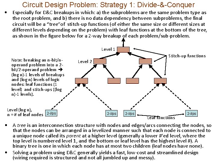
Circuit Design Problem: Strategy 1: Divide-&-Conquer • Especially for D&C breakups in which: a) the subproblems are the same problem type as the root problem, and b) there is no data dependency between subproblems, the final circuit will be a “tree”of stitch-up functions (of either the same size or different sizes at different levels depending on the problem) with leaf functions at the bottom of the tree, as shown in the figure below for a 2 -way breakup of each problem/sub-problem. Level 1 Note: breaking an n-bit/noperand problem into a 2 bit/2 -operand problem (log n)-1 levels of breakups and (log n) levels of logic nodes: leaf functions (1 level) and stitch-ups ((log n)-1 levels). Level (log n), n = # of leaf nodes 2 -i/ps Stitch-up functions Level 2 2 -i/ps Leaf functions 2 -i/ps • A tree is an interconnection structure with nodes and edges/arcs connecting the nodes, so that the nodes can be arranged in a levelized manner such that each node is connected to a unique node called its parent at a higher level (generally a lower #’ed level, where the top level is numbered level 1, and the bottom or leaf level has the highest level #). A binary tree is one in which each node has at most two children (leaf nodes have none). • Solving a problem using D&C generally yields a fast, low-cost and streamlined design (wiring required is structured and not all jumbled up and messy).

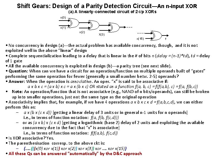
Shift Gears: Design of a Parity Detection Circuit—An n-input XOR (a) A linearly-connected circuit of 2 -i/p XORs x(0) x(1) x(2) X(3) x(15) f • No concurrency in design (a)---the actual problem has available concurrency, though, and it is not exploited well in the above “linear” design • Complete sequentialization leading to a delay that is linear in the # of bits n (delay = (n-1)*td), td = delay of 1 gate • All the available concurrency is exploited in design (b)---a parity tree (see next slide). • Question: When can we have a circuit for an operation/function on multiple operands built of “gates” performing the same operation for fewer (generally a small number betw. 2 -5) operands? • Answer: When the operation is associative. An oper. “x” is said to be associative if: a x b x c = (a x b) x c = a x (b x c) OR stated as a function f(a, b, c) = f(f(a, b), c) = f(a, f(b, c)) • Note: An operation/function that is not associative (e. g. , NAND of n bits/operands), can still be broken up into smaller operations, just not the same type as the original operation • Associativity implies that, for example, if we have 4 operations a x b x c x d = f(a, b, c, d), we can either perform this as: – a x (b x (c x d)) [getting a linear delay of 3 units or in general n-1 units for n operands] i. e. , in terms of function notation: f(a, f(b, f(c, d))) – or as (a x b) x (c x d) [getting a logarithmic (base 2) delay of 2 units and exploiting the available concurrency due to the fact that “x” is associative] i. e. , in terms of function notation: f(f(a, b), f(c, d)) • Is XOR associative? Yes. • The parenthesisation corresp. to the above ckt is: – (…. . (((x(0) xor x(1)) xor x(2)) xor x(3)) xor …. xor x(15)) • All these Qs can be answered “automatically” by the D&C approach

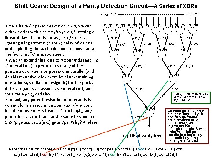
Shift Gears: Design of a Parity Detection Circuit—A Series of XORs x(15) x(14) • if we have 4 operations a x b x c x d, we can either perform this as a x (b x (c x d)) [getting a linear delay of 3 units] or as (a x b) x (c x d) [getting a logarithmic (base 2) delay of 2 units and exploiting the available concurrency due to the fact that “x” is associative]. • We can extend this idea to n operands (and n -1 operations) to perform as many of the pairwise operations as possible in parallel (and do this recursively for every level of remaining operations), similar to design (b) for the parity detector [xor is an associative operation!] and thus get a (log 2 n) delay. • In fact, any parenthesisation of operands is correct for an associative operation/function, but the above one is fastest. Surprisingly, any parenthesisation leads to the same h/w cost: n 1 2 -i/p gates, i. e. , 2(n-1) gate i/ps. Why? Analyze. x(1) x(0) w(3, 4) w(3, 6) w(2, 3) w(3, 1) w(3, 3) w(3, 5) w(3, 7) w(2, 2) w(1, 1) w(3, 2) w(2, 1) w(3, 0) w(2, 0) w(1, 0) Delay = (# of levels in AND-OR tree) * td = log 2 (n) *td w(0, 0) = f (b) 16 -bit parity tree An example of simple designer ingenuity. A bad design would have resulted in a linear delay, an ingenious (simple enough though) & well -informed design results in a log delay, and both have the same gate i/p cost Parenthesization of tree-circuit: (((x(15) xor x(14)) xor (x(13) xor x(12))) xor ((x(11) xor x(10)) xor (x(9) xor x(8)))) xor (((x(7) xor x(6)) xor (x(5) xor x(4))) xor ((x(3) xor x(2)) xor (x(1) xor x(0))))

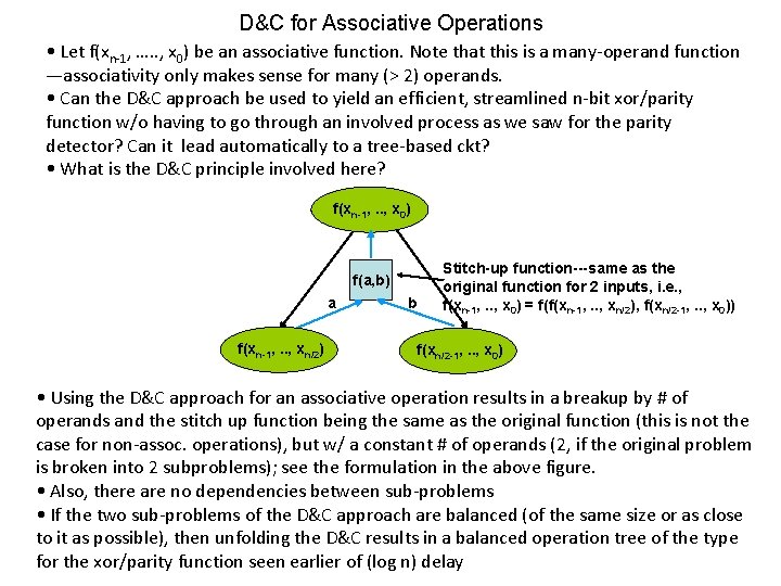
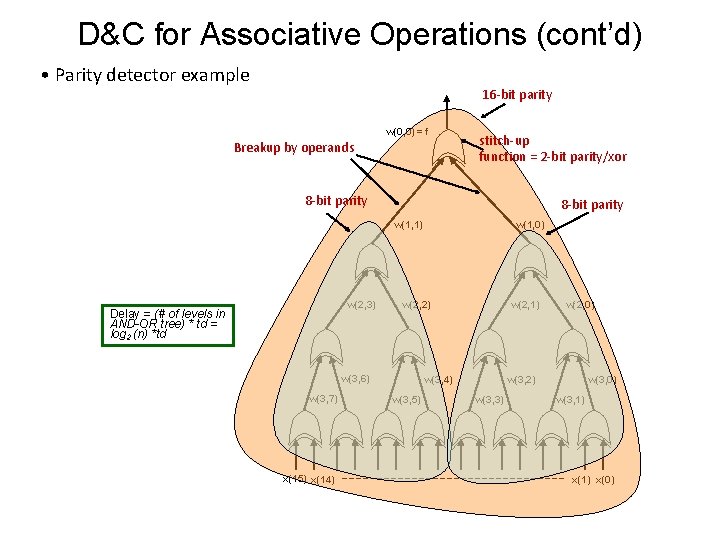
D&C for Associative Operations • Let f(xn-1, …. . , x 0) be an associative function. Note that this is a many-operand function —associativity only makes sense for many (> 2) operands. • Can the D&C approach be used to yield an efficient, streamlined n-bit xor/parity function w/o having to go through an involved process as we saw for the parity detector? Can it lead automatically to a tree-based ckt? • What is the D&C principle involved here? f(xn-1, . . , x 0) f(a, b) a f(xn-1, . . , xn/2) b Stitch-up function---same as the original function for 2 inputs, i. e. , f(xn-1, . . , x 0) = f(f(xn-1, . . , xn/2), f(xn/2 -1, . . , x 0)) f(xn/2 -1, . . , x 0) • Using the D&C approach for an associative operation results in a breakup by # of operands and the stitch up function being the same as the original function (this is not the case for non-assoc. operations), but w/ a constant # of operands (2, if the original problem is broken into 2 subproblems); see the formulation in the above figure. • Also, there are no dependencies between sub-problems • If the two sub-problems of the D&C approach are balanced (of the same size or as close to it as possible), then unfolding the D&C results in a balanced operation tree of the type for the xor/parity function seen earlier of (log n) delay

D&C for Associative Operations (cont’d) • Parity detector example 16 -bit parity w(0, 0) = f Breakup by operands stitch-up function = 2 -bit parity/xor 8 -bit parity w(1, 1) w(2, 3) Delay = (# of levels in AND-OR tree) * td = log 2 (n) *td w(2, 2) w(3, 6) w(3, 7) x(15) x(14) w(1, 0) w(2, 1) w(3, 4) w(3, 5) w(2, 0) w(3, 2) w(3, 3) w(3, 0) w(3, 1) x(0)

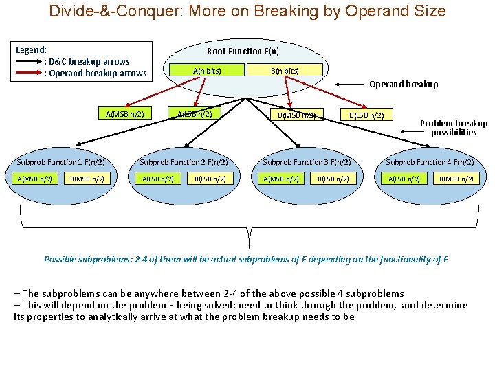
Divide-&-Conquer: More on Breaking by Operand Size Legend: : D&C breakup arrows : Operand breakup arrows A(MSB n/2) Root Function F(n) A(n bits) B(n bits) Operand breakup A(LSB n/2) B(MSB n/2) B(LSB n/2) Problem breakup possibilities Subprob Function 1 F(n/2) Subprob Function 2 F(n/2) Subprob Function 3 F(n/2) Subprob Function 4 F(n/2) A(MSB n/2) A(LSB n/2) B(MSB n/2) B(LSB n/2) B(MSB n/2) Possible subproblems: 2 -4 of them will be actual subproblems of F depending on the functionality of F – The subproblems can be anywhere between 2 -4 of the above possible 4 subproblems – This will depend on the problem F being solved: need to think through the problem, and determine its properties to analytically arrive at what the problem breakup needs to be

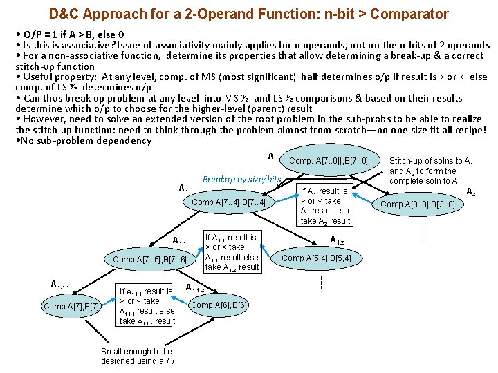
D&C Approach for a 2 -Operand Function: n-bit > Comparator • O/P = 1 if A > B, else 0 • Is this is associative? Issue of associativity mainly applies for n operands, not on the n-bits of 2 operands • For a non-associative function, determine its properties that allow determining a break-up & a correct stitch-up function • Useful property: At any level, comp. of MS (most significant) half determines o/p if result is > or < else comp. of LS ½ determines o/p • Can thus break up problem at any level into MS ½ and LS ½ comparisons & based on their results determine which o/p to choose for the higher-level (parent) result • However, need to solve an extended version of the root problem in the sub-probs to be able to realize the stitch-up function: need to think through the problem almost from scratch—no one size fit all recipe! • No sub-problem dependency A A 1 Breakup by size/bits Comp A[7. . 4], B[7. . 4] If A 1, 1 result is > or < take A 1, 1 result else take A 1, 2 result A 1, 1 Comp A[7. . 6], B[7. . 6] A 1, 1, 1 Comp A[7], B[7] If A 1, 1, 1 result is > or < take A 1, 1, 1 result else take A 1, 1, 2 result Small enough to be designed using a TT Comp. A[7. . 0]], B[7. . 0] A 1, 1, 2 Comp A[6], B[6] If A 1 result is > or < take A 1 result else take A 2 result A 1, 2 Comp A[5, 4], B[5, 4] Stitch-up of solns to A 1 and A 2 to form the complete soln to A A 2 Comp A[3. . 0], B[3. . 0]

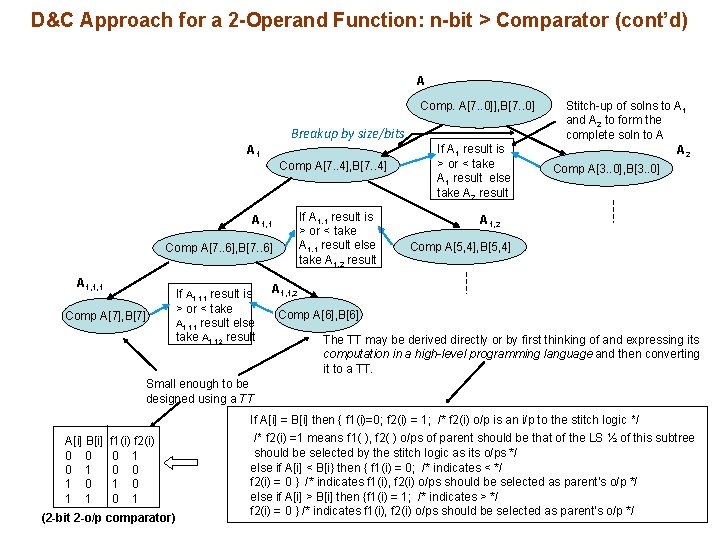
D&C Approach for a 2 -Operand Function: n-bit > Comparator (cont’d) A Comp. A[7. . 0]], B[7. . 0] Breakup by size/bits A 1 Comp A[7. . 4], B[7. . 4] If A 1, 1 result is > or < take A 1, 1 result else take A 1, 2 result A 1, 1 Comp A[7. . 6], B[7. . 6] A 1, 1, 1 Comp A[7], B[7] If A 1, 1, 1 result is > or < take A 1, 1, 1 result else take A 1, 1, 2 result If A 1 result is > or < take A 1 result else take A 2 result Stitch-up of solns to A 1 and A 2 to form the complete soln to A A 2 Comp A[3. . 0], B[3. . 0] A 1, 2 Comp A[5, 4], B[5, 4] A 1, 1, 2 Comp A[6], B[6] The TT may be derived directly or by first thinking of and expressing its computation in a high-level programming language and then converting it to a TT. Small enough to be designed using a TT If A[i] = B[i] then { f 1(i)=0; f 2(i) = 1; /* f 2(i) o/p is an i/p to the stitch logic */ A[i] B[i] 0 0 0 1 1 f 1(i) f 2(i) 0 1 0 0 1 (2 -bit 2 -o/p comparator) /* f 2(i) =1 means f 1( ), f 2( ) o/ps of parent should be that of the LS ½ of this subtree should be selected by the stitch logic as its o/ps */ else if A[i] < B[i} then { f 1(i) = 0; /* indicates < */ f 2(i) = 0 } /* indicates f 1(i), f 2(i) o/ps should be selected as parent’s o/p */ else if A[i] > B[i] then {f 1(i) = 1; /* indicates > */ f 2(i) = 0 } /* indicates f 1(i), f 2(i) o/ps should be selected as parent’s o/p */

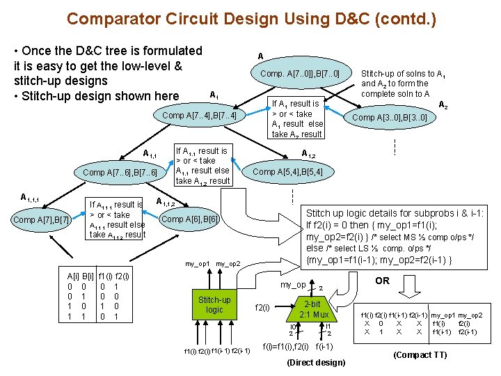
Comparator Circuit Design Using D&C (contd. ) • Once the D&C tree is formulated it is easy to get the low-level & stitch-up designs • Stitch-up design shown here A Comp. A[7. . 0]], B[7. . 0] A 1 If A 1 result is > or < take A 1 result else take A 2 result Comp A[7. . 4], B[7. . 4] If A 1, 1 result is > or < take A 1, 1 result else take A 1, 2 result A 1, 1 Comp A[7. . 6], B[7. . 6] A 1, 1, 1 Comp A[7], B[7] If A 1, 1, 1 result is > or < take A 1, 1, 1 result else take A 1, 1, 2 result f 1(i) f 2(i) 0 1 0 0 1 Comp A[3. . 0], B[3. . 0] A 1, 2 Comp A[5, 4], B[5, 4] A 1, 1, 2 Stitch up logic details for subprobs i & i-1: If f 2(i) = 0 then { my_op 1=f 1(i); my_op 2=f 2(i) } /* select MS ½ comp o/ps */ else /* select LS ½ comp. o/ps */ {my_op 1=f 1(i-1); my_op 2=f 2(i-1) } Comp A[6], B[6] my_op 1 my_op 2 A[i] B[i] 0 0 0 1 1 Stitch-up of solns to A 1 and A 2 to form the complete soln to A A 2 my_op Stitch-up logic 2 -bit 2: 1 Mux f 2(i) I 0 2 f 1(i) f 2(i) f 1(i-1) f 2(i-1) OR 2 I 1 2 f(i)=f 1(i), f 2(i) f(i-1) (Direct design) f 1(i) f 2(i) f 1(i-1) f 2(i-1) my_op 1 my_op 2 X 0 X X f 1(i) f 2(i) X 1 X X f 1(i-1) f 2(i-1) (Compact TT)

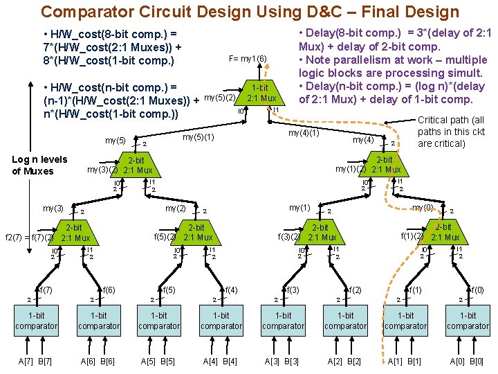
Comparator Circuit Design Using D&C – Final Design • H/W_cost(8 -bit comp. ) = 7*(H/W_cost(2: 1 Muxes)) + 8*(H/W_cost(1 -bit comp. ) F= my 1(6) • H/W_cost(n-bit comp. ) = (n-1)*(H/W_cost(2: 1 Muxes)) + n*(H/W_cost(1 -bit comp. )) my(5) Log n levels of Muxes I 0 I 1 my(4)(1) my(4) I 0 2 my(2) my(1) 2 I 0 2 2 f(6) 2 2 I 1 2 I 0 2 2 f(5) I 1 2 my(0) 2 f(4) 2 I 1 2 I 0 2 2 f(3) 2 2 -bit f(1)(2) 2: 1 Mux 2 -bit f(3)(2) 2: 1 Mux 2 -bit f(5)(2) 2: 1 Mux I 1 Critical path (all paths in this ckt are critical) 2 -bit my(1)(2) 2: 1 Mux 2 2 f(7) 2 I 0 I 1 2 -bit f 2(7) = f(7)(2) 2: 1 Mux 2 my(5)(2) 2 -bit my(3)(2) 2: 1 Mux 2 my(3) 1 -bit 2: 1 Mux my(5)(1) 2 • Delay(8 -bit comp. ) = 3*(delay of 2: 1 Mux) + delay of 2 -bit comp. • Note parallelism at work – multiple logic blocks are processing simult. • Delay(n-bit comp. ) = (log n)*(delay of 2: 1 Mux) + delay of 1 -bit comp. f(2) 2 I 1 2 f(1) 2 f(0) 2 1 -bit comparator 1 -bit comparator A[7] B[7] A[6] B[6] A[5] B[5] A[4] B[4] A[3] B[3] A[2] B[2] A[1] B[1] A[0] B[0]

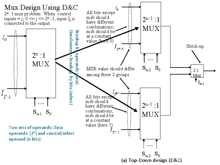
Mux Design Using D&C 2 n : 1 mux problem: When control inputs = j, 0 <= j <= 2 n -1, input Ij is connected to the output. 2 n : 1 MUX Breakup by operands (data) Simultaneous breakup by bits (select) I 0 Sn-1 S 0 Two sets of operands: Data operands (2 n) and control/select operand (n bits) All bits except msb should have different combinations; msb should be at a constant value (here 0) I 0 2 n-1 : 1 MUX Stitch-up n-1 MSB value should differ among these 2 groups Sn-2 S 0 2: 1 Mux Sn-1 I 2 n-1 n All bits except msb should have different combinations; msb should be at a constant value (here 1) 2 n-1 : 1 MUX Sn-2 S 0 (a) Top-Down design (D&C)

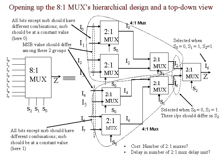
Opening up the 8: 1 MUX’s hierarchical design and a top-down view All bits except msb should have different combinations; msb should be at a constant value (here 0) MSB value should differ among these 2 groups I 0 I 1 I 2 I 3 I 4 I 5 I 6 I 7 I 0 I 1 I 2 8: 1 MUX Z I 3 S 2 S 1 S 0 All bits except msb should have different combinations; msb should be at a constant value (here 1) 2: 1 MUX I 5 Selected when S 0 = 0, S 1 = 1, S 2=1 S 0 I 2 2: 1 MUX S 0 I 4 I 04: 1 Mux 2: 1 MUX I 4 2: 1 MUX S 1 I 2 2: 1 MUX I 6 2: 1 I 7 MUX S 0 I 6 Z S 2 S 1 Selected when S 0 = 0, S 1 = 1. These i/ps should differ in S 2 S 0 I 6 2: 1 MUX I 6 4: 1 Mux • • Cost: Number of 2: 1 muxes? Delay in number of 2: 1 mux delay unit?

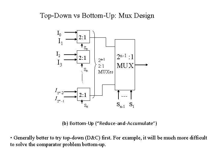
Top-Down vs Bottom-Up: Mux Design I 0 I 1 I 2 I 3 2 2: 1 S 0 2 n-1 2: 1 MUXes 2 n-1 : 1 MUX 2: 1 S 0 Sn-1 S 1 (b) Bottom-Up (“Reduce-and-Accumulate”) • Generally better to try top-down (D&C) first. For example, it will be much more difficult to solve the comparator problem bottom-up.

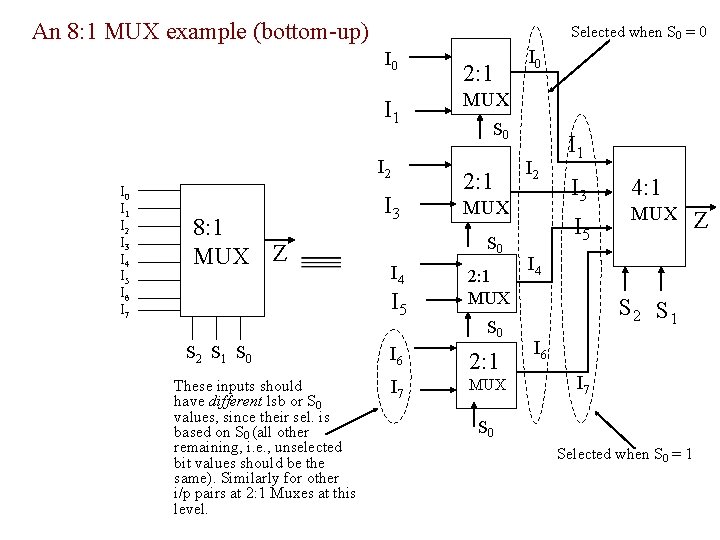
An 8: 1 MUX example (bottom-up) Selected when S 0 = 0 I 1 I 2 I 3 I 4 I 5 I 6 I 7 8: 1 MUX Z I 3 These inputs should have different lsb or S 0 values, since their sel. is based on S 0 (all other remaining, i. e. , unselected bit values should be the same). Similarly for other i/p pairs at 2: 1 Muxes at this level. MUX S 0 2: 1 I 4 I 2 MUX S 0 I 5 S 2 S 1 S 0 2: 1 I 0 2: 1 MUX S 0 I 6 2: 1 I 7 MUX I 1 I 3 I 5 4: 1 MUX I 4 S 2 S 1 I 6 I 7 S 0 Selected when S 0 = 1 Z

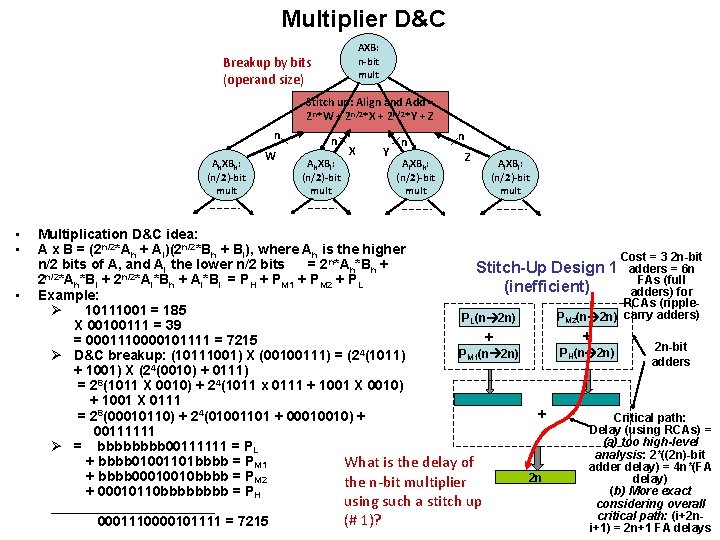
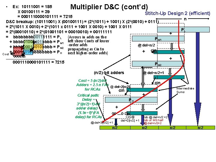
Multiplier D&C AXB: n-bit mult Breakup by bits (operand size) Stitch up: Align and Add = 2 n*W + 2 n/2*X + 2 n/2*Y + Z n Ah. XBh: (n/2)-bit mult • • • W n Ah. XBl: (n/2)-bit mult X Y n Al. XBh: (n/2)-bit mult n Z Al. XBl: (n/2)-bit mult Multiplication D&C idea: A x B = (2 n/2*Ah + Al)(2 n/2*Bh + Bl), where Ah is the higher Cost = 3 2 n-bit n/2 bits of A, and Al the lower n/2 bits = 2 n*Ah*Bh + adders = 6 n Stitch-Up Design 1 FAs (full 2 n/2*Ah*Bl + 2 n/2*Al*Bh + Al*Bl = PH + PM 1 + PM 2 + PL (inefficient) adders) for Example: RCAs (rippleØ 10111001 = 185 PM 2(n 2 n) carry adders) PL(n 2 n) X 00100111 = 39 + + = 0001110000101111 = 7215 2 n-bit 4 PH(n 2 n) PM 1(n 2 n) Ø D&C breakup: (10111001) X (00100111) = (2 (1011) adders + 1001) X (24(0010) + 0111) = 28(1011 X 0010) + 24(1011 x 0111 + 1001 X 0010) + 1001 X 0111 + = 28(00010110) + 24(01001101 + 00010010) + Critical path: Delay (using RCAs) = 00111111 (a) too high-level Ø = bbbb 00111111 = PL analysis: 2*((2 n)-bit + bbbb 01001101 bbbb = PM 1 What is the delay of adder delay) = 4 n*(FA + bbbb 00010010 bbbb = PM 2 2 n delay) the n-bit multiplier (b) More exact + 00010110 bbbb = PH using such a stitch up considering overall ___________ critical path: (i+2 n(# 1)? 0001110000101111 = 7215 i+1) = 2 n+1 FA delays

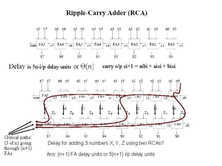
FA 7 carry o/p ci+1 = aibi + aici + bici is 5 n-i/p delay units FA 7 z 6 z 5 z 4 z 3 z 2 z 1 FA 7 Critical paths (3 of n) going through (n+1) FAs Delay for adding 3 numbers X, Y, Z using two RCAs? Ans: (n+1) FA delay units or 5(n+1) i/p delay units z 0

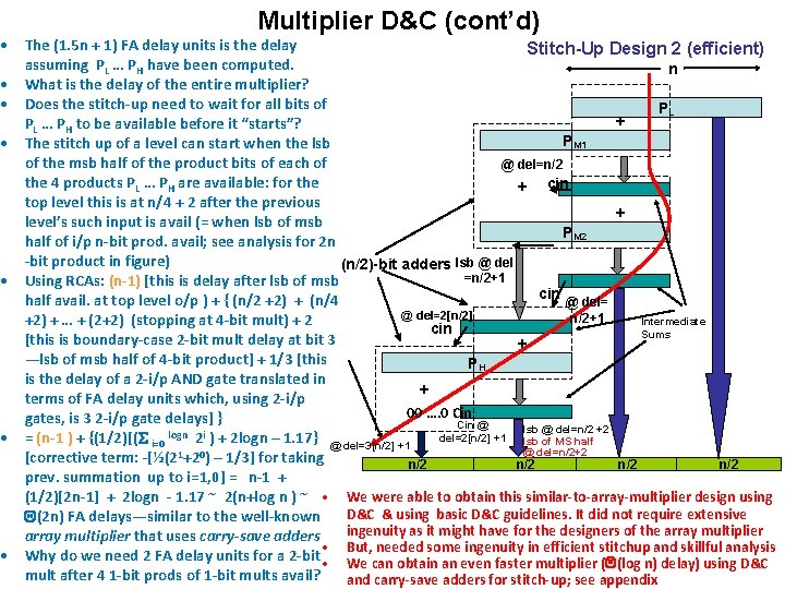
• Multiplier D&C (cont’d) Ex: 10111001 = 185 X 00100111 = 39 Stitch-Up Design 2 (efficient) = 0001110000101111 = 7215 n D&C breakup: (10111001) X (00100111) = (24(1011) + 1001) X (24(0010) + 0111) = 28(1011 X 0010) + 24(1011 x 0111 + 1001 X 0010) + 1001 X 0111 PL = 28(00010110) + 24(01001101 + 00010010) + 00111111 + = bbbb 00111111 = PL (Arrows in adds on the PM 1 + bbbb 01001101 bbbb = PM 1 left show Couts of lower adds @ del=n/2 + bbbb 00010010 bbbb = PM 2 -order propagating as Cin to + cin + 00010110 bbbb = PH next higher-order adds) Cout 000 Cin ___________ + 0001110000101111 = 7215 P M 2 (n/2)-bit adders @ del=n/2+1 Cost = 5 (n/2)-bit Adders = 2. 5 n FAs @ del=2[n/2] for RCAs cin Critical path: Delay = 3*((n/2)+1)-bit adder delay) = (1. 5 n+1)*(FA delay) for RCAs cin Intermediate Sums + PH + 00 …. 0 Cin @ del=3[n/2] +1 n/2 Cin @ del=2[n/2] +1 lsb @ del=n/2 +2 lsb of MS half @ del=n/2+2 n/2 n/2

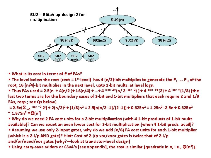
Multiplier D&C (cont’d) • The (1. 5 n + 1) FA delay units is the delay Stitch-Up Design 2 (efficient) assuming PL … PH have been computed. n • What is the delay of the entire multiplier? • Does the stitch-up need to wait for all bits of PL + PL … PH to be available before it “starts”? PM 1 • The stitch up of a level can start when the lsb of the msb half of the product bits of each of @ del=n/2 the 4 products PL … PH are available: for the + cin top level this is at n/4 + 2 after the previous + level’s such input is avail (= when lsb of msb PM 2 half of i/p n-bit prod. avail; see analysis for 2 n -bit product in figure) (n/2)-bit adders lsb @ del =n/2+1 • Using RCAs: (n-1) [this is delay after lsb of msb cin half avail. at top level o/p ) + { (n/2 +2) + (n/4 @ del=2[n/2] n/2+1 Intermediate +2) + … + (2+2) (stopping at 4 -bit mult) + 2 cin Sums [this is boundary-case 2 -bit mult delay at bit 3 + —lsb of msb half of 4 -bit product] + 1/3 [this PH is the delay of a 2 -i/p AND gate translated in + terms of FA delay units which, using 2 -i/p 00 …. 0 Cin gates, is 3 2 -i/p gate delays] } Cin @ lsb @ del=n/2 +2 del=2[n/2] +1 • = (n-1 ) + {(1/2)[(S i=0 logn 2 i ) + 2 logn – 1. 17} @ del=3[n/2] +1 lsb of MS half @ del=n/2+2 1 0 [corrective term: -[½(2 +2 ) – 1/3] for taking n/2 n/2 prev. summation up to i=1, 0] = n-1 + (1/2)[2 n-1] + 2 logn - 1. 17 ~ 2(n+log n ) ~ • We were able to obtain this similar-to-array-multiplier design using D&C & using basic D&C guidelines. It did not require extensive Q(2 n) FA delays—similar to the well-known ingenuity as it might have for the designers of the array multiplier that uses carry-save adders • But, needed some ingenuity in efficient stitchup and skillful analysis • Why do we need 2 FA delay units for a 2 -bit • We can obtain an even faster multiplier (Q(log n) delay) using D&C mult after 4 1 -bit prods of 1 -bit mults avail? and carry-save adders for stitch-up; see appendix

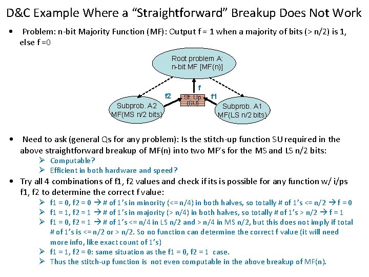
2 n SU 2 = Stitch up design 2 for multiplication SU 2(n) n SU 2(n/2) n/2 SU 2 (n/4) • What is its cost in terms of # of FAs? • The level below the root (root = 1 st level) has 4 (n/2)-bit multiplies to generate the PL …. PH of the root, 16 (n/4)-bit multiplies in the next level, upto 2 -bit mults. at level logn. • Thus FAs used = 2. 5[n + 4(n/2 )+ 16(n/4) + …+ 4 logn -2*(n/ 2 logn -2) ] + 4 logn -1*(2) + 4 logn *(1/8) [the last two terms are for the boundary cases of 2 -bit and 1 -bit multipliers that each require 2 and 1/8 FAs, resp. ; see Qs below) = 2. 5 n(S i=0 logn – 2 2 i) + 2(n/2)2 + (1/8)n 2 = 2. 5[n(n/2 -1]/(2 -1)) + 0. 625 n 2 = 1. 25 n 2 -2. 5 n + 0. 625 n 2 ~ 1. 875 n 2 = Q(n 2) • Why do we need 2 FA cost units for a 2 -bit multiplication (with 4 1 -bit products of 1 -bit mults available)? Can we count an even lower cost for 2 -bit multiplication (when 4 1 -bit prods. avail)? • Assuming we use only 2 -input gates, why do we add (n/8) FA cost units for each 1 -bit multiplier (which is a 2 -i/p AND gate)? Hint: Cost of 2 -i/p xor/xnor gates is twice that of 2 -i/p and/or/nand/nor gates (why? —look at transistor-level design) • Using carry-save adders or CSv. A’s [see appendix], the cost is similar (quadratic in n, i. e. , Q(n 2)).

D&C Example Where a “Straightforward” Breakup Does Not Work • Problem: n-bit Majority Function (MF): Output f = 1 when a majority of bits (> n/2) is 1, else f =0 Root problem A: n-bit MF [MF(n)] f f 2 Subprob. A 2 MF(MS n/2 bits) St. Up (SU) f 1 Subprob. A 1 MF(LS n/2 bits) • Need to ask (general Qs for any problem): Is the stitch-up function SU required in the above straightforward breakup of MF(n) into two MF’s for the MS and LS n/2 bits: Ø Computable? Ø Efficient in both hardware and speed? • Try all 4 combinations of f 1, f 2 values and check if its is possible for any function w/ i/ps f 1, f 2 to determine the correct f value: Ø f 1 = 0, f 2 = 0 # of 1’s in minority (<= n/4) in both halves, so totally # of 1’s <= n/2 f = 0 Ø f 1 = 1, f 2 = 1 # of 1’s in majority (> n/4) in both halves, so totally # of 1’s > n/2 f = 1 Ø f 1 = 0, f 2 = 1 # of 1’s <= n/4 in LS n/2 and > n/4 in MS n/2, but this does not imply if total # of 1’s is <= n/2 or > n/2. So no function can determine the correct f value (it will need more info, like exact count of 1’s) Ø f 1 = 1, f 2 = 0: same situation as the f 1 = 0, f 2 = 1 case. Ø Thus the stitch-up function is not even computable in the above breakup of MF(n).

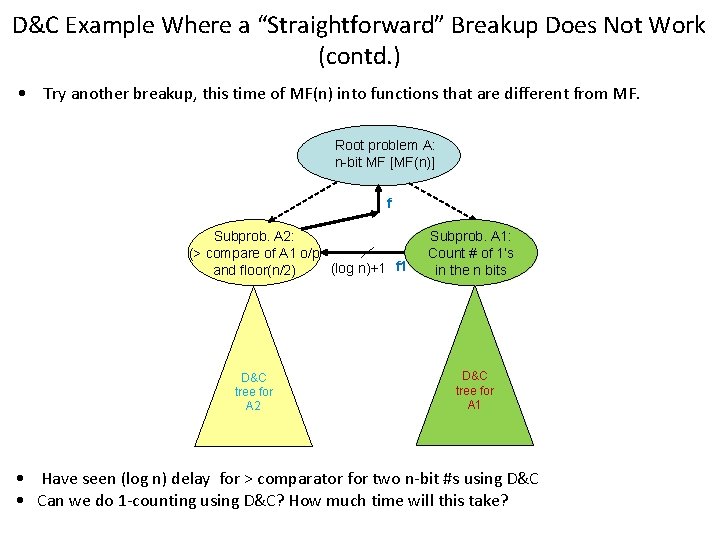
D&C Example Where a “Straightforward” Breakup Does Not Work (contd. ) • Try another breakup, this time of MF(n) into functions that are different from MF. Root problem A: n-bit MF [MF(n)] f Subprob. A 2: (> compare of A 1 o/p (log n)+1 f 1 and floor(n/2) D&C tree for A 2 Subprob. A 1: Count # of 1’s in the n bits D&C tree for A 1 • Have seen (log n) delay for > comparator for two n-bit #s using D&C • Can we do 1 -counting using D&C? How much time will this take?

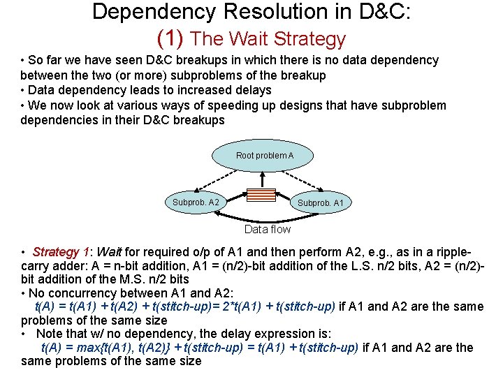
Dependency Resolution in D&C: (1) The Wait Strategy • So far we have seen D&C breakups in which there is no data dependency between the two (or more) subproblems of the breakup • Data dependency leads to increased delays • We now look at various ways of speeding up designs that have subproblem dependencies in their D&C breakups Root problem A Subprob. A 2 Subprob. A 1 Data flow • Strategy 1: Wait for required o/p of A 1 and then perform A 2, e. g. , as in a ripplecarry adder: A = n-bit addition, A 1 = (n/2)-bit addition of the L. S. n/2 bits, A 2 = (n/2)bit addition of the M. S. n/2 bits • No concurrency between A 1 and A 2: t(A) = t(A 1) + t(A 2) + t(stitch-up)= 2*t(A 1) + t(stitch-up) if A 1 and A 2 are the same problems of the same size • Note that w/ no dependency, the delay expression is: t(A) = max{t(A 1), t(A 2)} + t(stitch-up) = t(A 1) + t(stitch-up) if A 1 and A 2 are the same problems of the same size

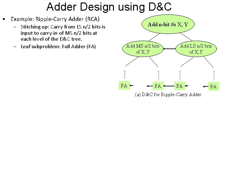
Adder Design using D&C • Example: Ripple-Carry Adder (RCA) – Stitching up: Carry from LS n/2 bits is input to carry-in of MS n/2 bits at each level of the D&C tree. – Leaf subproblem: Full Adder (FA) Add n-bit #s X, Y Add MS n/2 bits of X, Y FA FA Add LS n/2 bits of X, Y FA (a) D&C for Ripple-Carry Adder FA

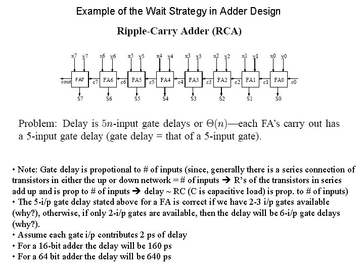
Example of the Wait Strategy in Adder Design FA 7 • Note: Gate delay is propotional to # of inputs (since, generally there is a series connection of transistors in either the up or down network = # of inputs R’s of the transistors in series add up and is prop to # of inputs delay ~ RC (C is capacitive load) is prop. to # of inputs) • The 5 -i/p gate delay stated above for a FA is correct if we have 2 -3 i/p gates available (why? ), otherwise, if only 2 -i/p gates are available, then the delay will be 6 -i/p gate delays (why? ). • Assume each gate i/p contributes 2 ps of delay • For a 16 -bit adder the delay will be 160 ps • For a 64 bit adder the delay will be 640 ps

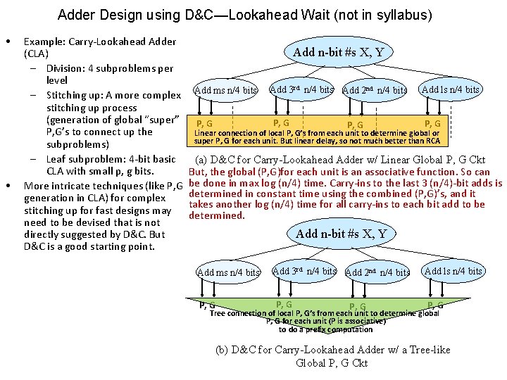
Adder Design using D&C—Lookahead Wait (not in syllabus) • • Example: Carry-Lookahead Adder (CLA) – Division: 4 subproblems per level – Stitching up: A more complex stitching up process (generation of global “super” P, G’s to connect up the subproblems) – Leaf subproblem: 4 -bit basic CLA with small p, g bits. More intricate techniques (like P, G generation in CLA) for complex stitching up for fast designs may need to be devised that is not directly suggested by D&C. But D&C is a good starting point. Add n-bit #s X, Y Add ms n/4 bits Add 3 rd n/4 bits Add 2 nd n/4 bits P, G Add ls n/4 bits P, G Linear connection of local P, G’s from each unit to determine global or super P, G for each unit. But linear delay, so not much better than RCA (a) D&C for Carry-Lookahead Adder w/ Linear Global P, G Ckt But, the global (P, G)for each unit is an associative function. So can be done in max log (n/4) time. Carry-ins to the last 3 (n/4)-bit adds is determined in constant time using the combined (P, G)’s, and it takes another log (n/4) time for all carry-ins to each bit add to be determined. Add n-bit #s X, Y Add ms n/4 bits P, G Add 3 rd n/4 bits Add 2 nd n/4 bits P, G Add ls n/4 bits P, G Tree connection of local P, G’s from each unit to determine global P, G for each unit (P is associative) to do a prefix computation (b) D&C for Carry-Lookahead Adder w/ a Tree-like Global P, G Ckt

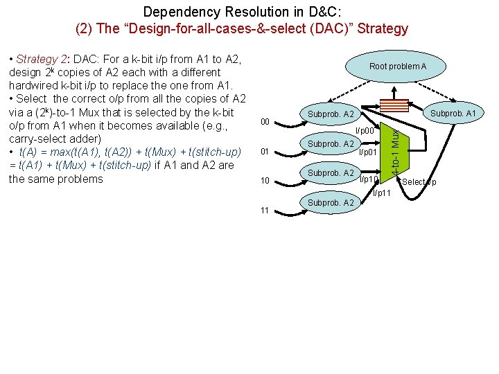
Dependency Resolution in D&C: (2) The “Design-for-all-cases-&-select (DAC)” Strategy Root problem A 00 01 10 Subprob. A 1 Subprob. A 2 I/p 00 Subprob. A 2 I/p 01 I/p 10 4 -to-1 Mux • Strategy 2: DAC: For a k-bit i/p from A 1 to A 2, design 2 k copies of A 2 each with a different hardwired k-bit i/p to replace the one from A 1. • Select the correct o/p from all the copies of A 2 via a (2 k)-to-1 Mux that is selected by the k-bit o/p from A 1 when it becomes available (e. g. , carry-select adder) • t(A) = max(t(A 1), t(A 2)) + t(Mux) + t(stitch-up) = t(A 1) + t(Mux) + t(stitch-up) if A 1 and A 2 are the same problems I/p 11 11 Subprob. A 2 Select i/p

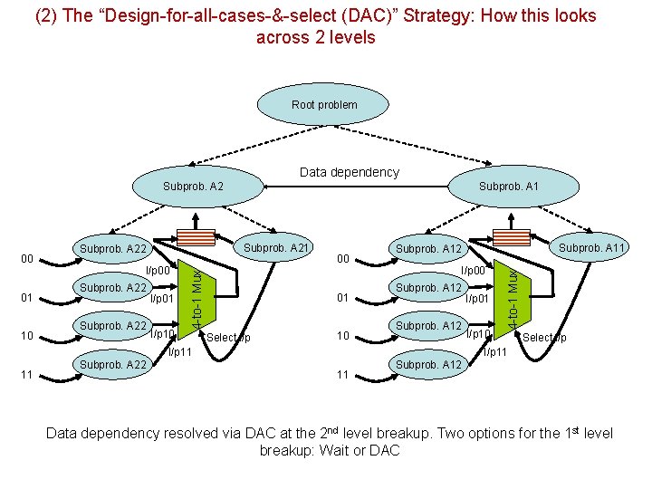
(2) The “Design-for-all-cases-&-select (DAC)” Strategy: How this looks across 2 levels Root problem Data dependency Subprob. A 2 10 I/p 00 Subprob. A 22 I/p 01 I/p 10 00 01 Select i/p 10 I/p 00 Subprob. A 12 I/p 11 11 Subprob. A 22 Subprob. A 11 Subprob. A 12 I/p 01 I/p 10 4 -to-1 Mux 01 Subprob. A 22 4 -to-1 Mux 00 Subprob. A 1 Select i/p I/p 11 11 Subprob. A 12 Data dependency resolved via DAC at the 2 nd level breakup. Two options for the 1 st level breakup: Wait or DAC

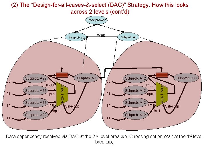
(2) The “Design-for-all-cases-&-select (DAC)” Strategy: How this looks across 2 levels (cont’d) Root problem 01 10 Subprob. A 21 Subprob. A 22 I/p 00 Subprob. A 22 I/p 01 I/p 10 4 -to-1 Mux 00 Wait Subprob. A 1 00 01 Select i/p 10 I/p 00 Subprob. A 12 11 I/p 01 I/p 10 Select i/p I/p 11 Subprob. A 22 Subprob. A 11 Subprob. A 12 4 -to-1 Mux Subprob. A 2 11 Subprob. A 12 Data dependency resolved via DAC at the 2 nd level breakup. Choosing option Wait at the 1 st level breakup,

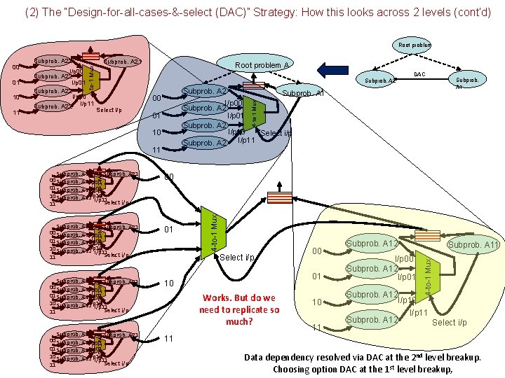
(2) The “Design-for-all-cases-&-select (DAC)” Strategy: How this looks across 2 levels (cont’d) Root problem Subprob. A 2 Subprob. A 1 I/p 00 Subprob. A 2 I/p 01 Subprob. A 2 I/p 10 Select i/p I/p 11 Subprob. A 22 Subprob. A 21 00 Subprob. A 22 I/p 00 01 Subprob. A 22 I/p 01 10 Subprob. A 22 I/p 10 I/p 11 Select i/p 11 00 Subprob. A 22 Subprob. A 21 00 Subprob. A 22 I/p 00 01 Subprob. A 22 I/p 01 10 Subprob. A 22 I/p 10 I/p 11 Select i/p 11 01 Subprob. A 22 Subprob. A 21 00 Subprob. A 22 I/p 00 01 Subprob. A 22 I/p 01 10 Subprob. A 22 I/p 10 I/p 11 Select i/p 11 10 4 -to-1 Mux 01 10 Subprob. A 22 Subprob. A 21 00 Subprob. A 22 I/p 00 01 Subprob. A 22 I/p 01 10 Subprob. A 22 I/p 10 I/p 11 Select i/p 11 Subprob. A 1 4 -to-1 Mux 00 Select i/p DAC Select i/p 00 01 Works. But do we need to replicate so much? 10 11 Subprob. A 12 I/p 00 Subprob. A 12 I/p 01 Subprob. A 11 4 -to-1 Mux Root problem A Subprob. A 2 4 -to-1 Mux 11 I/p 00 Subprob. A 22 I/p 01 Subprob. A 22 I/p 10 Subprob. A 22 I/p 11 4 -to-1 Mux 10 Subprob. A 21 4 -to-1 Mux 01 Subprob. A 22 4 -to-1 Mux 00 Subprob. A 12 I/p 10 I/p 11 Subprob. A 12 Select i/p 11 Data dependency resolved via DAC at the 2 nd level breakup. Choosing option DAC at the 1 st level breakup,

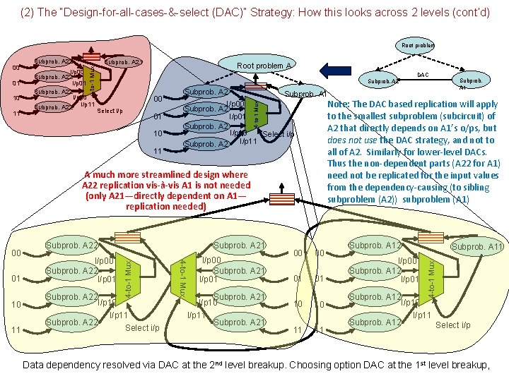
(2) The “Design-for-all-cases-&-select (DAC)” Strategy: How this looks across 2 levels (cont’d) Root problem 11 I/p 00 Subprob. A 22 I/p 01 Subprob. A 22 I/p 10 Subprob. A 22 I/p 11 Root problem A Subprob. A 2 00 Select i/p 01 10 11 Subprob. A 2 10 11 4 -to-1 Mux Subprob. A 22 I/p 10 I/p 11 Subprob. A 22 Select i/p 4 -to-1 Mux 01 Subprob. A 22 I/p 00 Subprob. A 22 I/p 01 Subprob. A 1 I/p 00 Note: The DAC based replication will apply Subprob. A 2 to the smallest subproblem (subcircuit) of I/p 01 Subprob. A 2 that directly depends on A 1’s o/ps, but I/p 10 Select i/p does not use the DAC strategy, and not to I/p 11 Subprob. A 2 all of A 2. Similarly for lower-level DACs. Thus the non-dependent parts (A 22 for A 1) need not be replicated for the input values from the dependency-causing (to sibling subproblem (A 2)) subproblem (A 1) A much more streamlined design where A 22 replication vis-à-vis A 1 is not needed (only A 21—directly dependent on A 1— replication needed) 00 DAC I/p 00 Subprob. A 21 I/p 01 Subprob. A 21 I/p 10 I/p 11 Subprob. A 21 00 00 01 01 10 10 11 11 Subprob. A 12 I/p 00 Subprob. A 12 I/p 01 Subprob. A 11 4 -to-1 Mux 10 Subprob. A 21 4 -to-1 Mux 01 Subprob. A 22 4 -to-1 Mux 00 Subprob. A 12 I/p 10 I/p 11 Subprob. A 12 Select i/p Data dependency resolved via DAC at the 2 nd level breakup. Choosing option DAC at the 1 st level breakup,

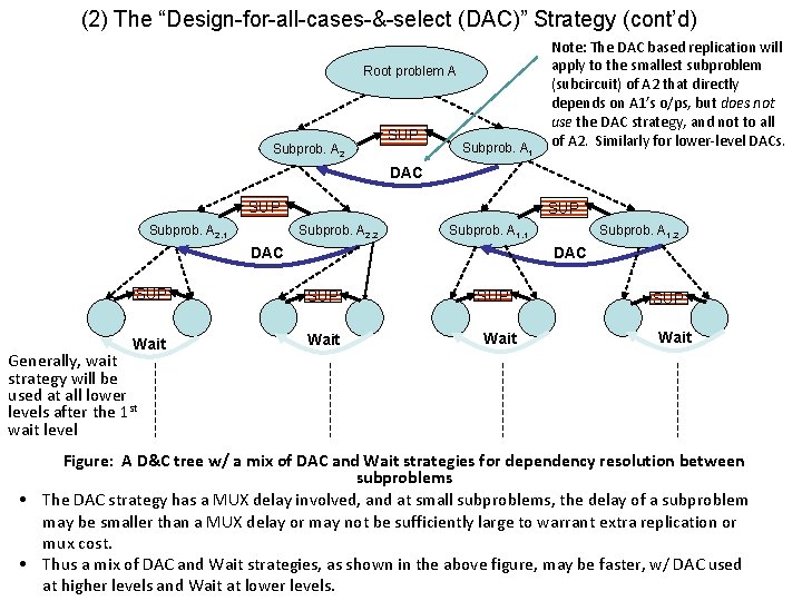
(2) The “Design-for-all-cases-&-select (DAC)” Strategy (cont’d) Root problem A Subprob. A 2 SUP Subprob. A 1 Note: The DAC based replication will apply to the smallest subproblem (subcircuit) of A 2 that directly depends on A 1’s o/ps, but does not use the DAC strategy, and not to all of A 2. Similarly for lower-level DACs. DAC SUP Subprob. A 2, 1 SUP Subprob. A 2, 2 Subprob. A 1, 1 Subprob. A 1, 2 DAC SUP Wait Generally, wait strategy will be used at all lower levels after the 1 st wait level Figure: A D&C tree w/ a mix of DAC and Wait strategies for dependency resolution between subproblems • The DAC strategy has a MUX delay involved, and at small subproblems, the delay of a subproblem may be smaller than a MUX delay or may not be sufficiently large to warrant extra replication or mux cost. • Thus a mix of DAC and Wait strategies, as shown in the above figure, may be faster, w/ DAC used at higher levels and Wait at lower levels.

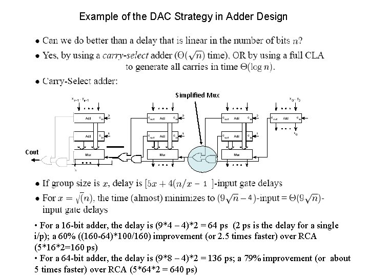
Example of the DAC Strategy in Adder Design Simplified Mux Cout 1 4 • For a 16 -bit adder, the delay is (9*4 – 4)*2 = 64 ps (2 ps is the delay for a single i/p); a 60% ((160 -64)*100/160) improvement (or 2. 5 times faster) over RCA (5*16*2=160 ps) • For a 64 -bit adder, the delay is (9*8 – 4)*2 = 136 ps; a 79% improvement (or about 5 times faster) over RCA (5*64*2 = 640 ps)

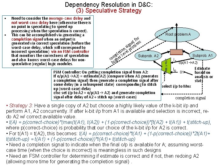
Dependency Resolution in D&C: (3) Speculative Strategy • • or lf m a ign oble s on el pr i t pler lev Subprob. A 2 m co ighe h Root problem A 2 -to-1 Mux Need to consider the average-case delay and not worst-case delay here (otherwise there is no point in speculating to speed up processing when the speculation is correct). This can be accomplished via generating a completion signal when an output is generated via correct speculation (before the worst-case delay, which will correspond to incorrect speculation) via an FSM controller that monitors the correctness of speculation and also knows worst-case delays for nonspeculative (regular) logic modules. I 1 Subprob. A 1 op(A 1 A 2) Estimate I 0 FSM Controller: On getting completion signal from A 2: 01 based on If o/p(A 1 A 2) = estimate(A 2) (compare when A 1 generates analysis or a completion signal) then generate a completion signal after stats some delay (in a subsequent state) corresponding to stitch select i/p to Mux up (worst-case) delay else set i/p to A 2 = o/p(A 1 A 2) and generate completion signal after delay of A 2 + stitch up (worst-cases) completion signal • Strategy 3: Have a single copy of A 2 but choose a highly likely value of the k-bit i/p and perform A 1, A 2 concurrently. If after k-bit i/p from A 1 is available and selection is incorrect, redo A 2 w/ correct available value. • t(A) = p(correct-choice)*(max(t(A 1), t(A 2)) + (1 -p(correct-choice))*[t(A 2) + t(A 1)) + t(stitch-up), where p(correct-choice) is probability that our choice of the k-bit i/p for A 2 is correct. • For t(A 1) = t(A 2), this becomes: t(A) = p(correct-choice)*t(A 1) + (1 -p(correct-choice))*2 t(A 1)+ t(stitch-up) = t(A 1) + (1 -p(correct-choice))*t(A 1)+ t(stitch-up) • Need a completion signal to indicate when the final o/p is available for A; assuming worstcase time (when the choice is incorrect) is meaningless in such designs • Need an FSM controller for determining if estimate is correct and if not, then redoing A 2 (allowing more time for generating the completion signal).

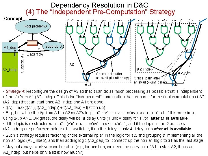
Dependency Resolution in D&C: (4) The “Independent Pre-Computation” Strategy Concept v’ x’ u v x w’ x yw z’ a 1 u’ x a 1 v’ x’ u v x w’ x yw z’ u’ x a 1 Root problem A A 2_dep Subprob. A 2_indep a 1 Subprob. A 1 Data flow A 2_indep Critical path after a 1 avail (8 -unit delay) a 2 Critical path after a 1 avail (4 -unit delay) A 2_dep a 2 • Strategy 4: Reconfigure the design of A 2 so that it can do as much processing as possible that is independent of the i/p from A 1 (A 2_indep). This is the “independent” computation that prepares for the final computation of A 2 (A 2_dep) that can start once A 2_indep and A 1 are done. • t(A) = max(t(A 1), t(A 2_indep)) + t(A 2_dep) + t(stitch-up) • E. g. , Let a 1 be the i/p from A 1 to A 2 w/ A 2’s logic: a 2 = v’x’ + uvx + w’xy + wz’a 1 + u’xa 1. If this were impl. using 2 -i/p AND/OR gates, the delay will be 8 delay units (1 unit = delay for 1 i/p) after a 1 is available. • If the logic is re-structured as a 2= (v’x’ + uvx + w’xy) + (wz’ + u’x)a 1, and if the logic in the 2 brackets (A 2_indep) are performed before a 1 is available, then the delay is only 4 delay units after a 1 is available. • Such a strategy requires factoring of the external i/p a 1 in the logic for a 2, and grouping & implementing all the non-a 1 logic (A 2_indep), and then adding logic (A 2_dep) to “connect” up the non-a 1 logic to a 1 as the last stage. • May not always work very well or at all (e. g, for addition, we need the carry out of A 1 to start A 2; it has an A 2_indep, but helps only a little; how much? )

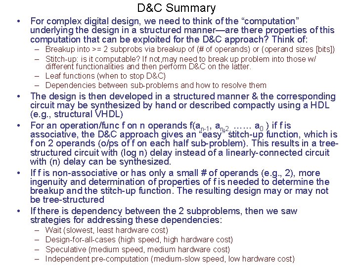
D&C Summary • For complex digital design, we need to think of the “computation” underlying the design in a structured manner—are there properties of this computation that can be exploited for the D&C approach? Think of: – Breakup into >= 2 subprobs via breakup of (# of operands) or (operand sizes [bits]) – Stitch-up: is it computable? If not, may need to break up problem into those w/ different functionalities and then perform D&C on the latter. – Leaf functions (when to stop D&C) – Dependencies between sub-problems and how to resolve them • • The design is then developed in a structured manner & the corresponding circuit may be synthesized by hand or described compactly using a HDL (e. g. , structural VHDL) For an operation/func f on n operands f(an-1, an-2, …… a 0 ) if f is associative, the D&C approach gives an “easy” stitch-up function, which is f on 2 operands (o/ps of f on each half sub-problem). This results in a treestructured circuit with (log n) delay instead of a linearly-connected circuit with (n) delay can be synthesized. If f is non-associative or has only a small # of operands (e. g. , 2), more ingenuity and determination of properties of f is needed to determine the breakup and the stitch-up function. The resulting design may or may not be tree-structured If there is dependency between the 2 subproblems, then we saw strategies for addressing these dependencies: – – Wait (slowest, least hardware cost) Design-for-all-cases (high speed, high hardware cost) Speculative (medium speed, medium hardware cost) Independent pre-computation (medium-slow speed, low hardware cost)

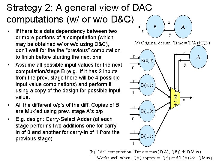
Strategy 2: A general view of DAC computations (w/ or w/o D&C) • • • If there is a data dependency between two or more portions of a computation (which may be obtained w/ or w/o using D&C), don’t wait for the “previous” computation to finish before starting the next one Assume all possible input values for the next computation/stage B (e. g. , if it has 2 inputs from the prev. stage there will be 4 possible input value combinations) and perform it using a copy of the design for possible input value. All the different o/p’s of the diff. Copies of B are Mux’ed using prev. stage A’s o/p E. g. design: Carry-Select Adder (at each stage performs two additions one for carryin of 0 and another for carry-in of 1 from the previous stage) B A y (a) Original design: Time = T(A)+T(B) 0 x B(0, 0) 0 B(0, 1) 1 1 A y 0 4: 1 Mux • z x z B(1, 0) 0 1 B(1, 1) 1 (b) DAC computation: Time = max(T(A), T(B)) + T(Mux). Works well when T(A) approx = T(B) and T(A) >> T(Mux)

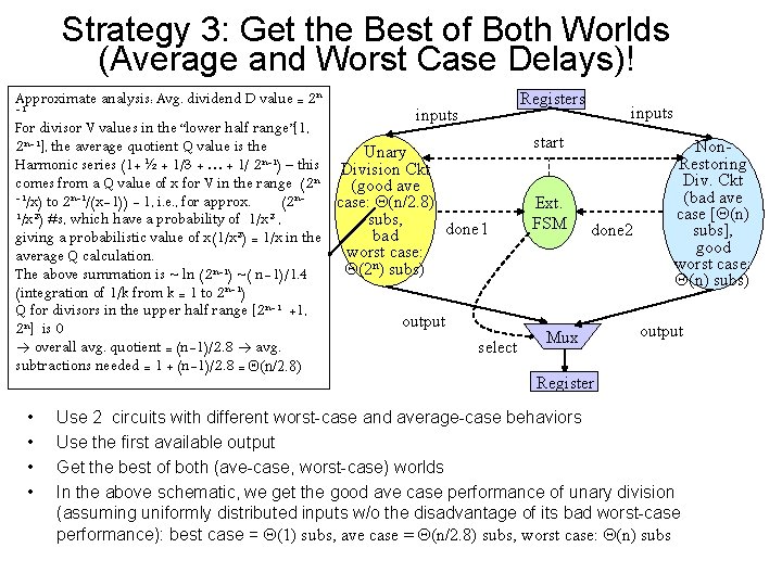
Strategy 3: Get the Best of Both Worlds (Average and Worst Case Delays)! Approximate analysis: Avg. dividend D value = 2 n -1 inputs Registers inputs For divisor V values in the “lower half range”[1, start 2 n-1], the average quotient Q value is the Non. Unary n-1 Restoring Harmonic series (1+ ½ + 1/3 + … + 1/ 2 ) – this Division Ckt Div. Ckt comes from a Q value of x for V in the range (2 n (good ave -1/x) to 2 n-1/(x-1)) - 1, i. e. , for approx. (bad ave (2 ncase: Q(n/2. 8) Ext. case [Q(n) 1/x 2) #s, which have a probability of 1/x 2 , subs, FSM done 2 done 1 subs], bad giving a probabilistic value of x(1/x 2) = 1/x in the good worst case: average Q calculation. n worst case: Q(2 ) subs) The above summation is ~ ln (2 n-1) ~( n-1)/1. 4 Q(n) subs) (integration of 1/k from k = 1 to 2 n-1) Q for divisors in the upper half range [2 n-1 +1, output 2 n] is 0 output Mux overall avg. quotient = (n-1)/2. 8 avg. select subtractions needed = 1 + (n-1)/2. 8 = Q(n/2. 8) Register • • Use 2 circuits with different worst-case and average-case behaviors Use the first available output Get the best of both (ave-case, worst-case) worlds In the above schematic, we get the good ave case performance of unary division (assuming uniformly distributed inputs w/o the disadvantage of its bad worst-case performance): best case = Q(1) subs, ave case = Q(n/2. 8) subs, worst case: Q(n) subs

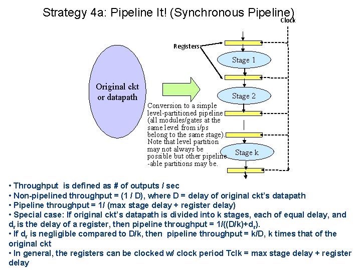
Strategy 4 a: Pipeline It! (Synchronous Pipeline) Clock Registers Stage 1 Original ckt or datapath Stage 2 Conversion to a simple level-partitioned pipeline (all modules/gates at the same level from i/ps belong to the same stage). Note that level partition may not always be possible but other pipeline -able partitions may be. Stage k • Throughput is defined as # of outputs / sec • Non-pipelined throughput = (1 / D), where D = delay of original ckt’s datapath • Pipeline throughput = 1/ (max stage delay + register delay) • Special case: If original ckt’s datapath is divided into k stages, each of equal delay, and dr is the delay of a register, then pipeline throughput = 1/((D/k)+d r). • If dr is negligible compared to D/k, then pipeline throughput = k/D, k times that of the original ckt • In general, the registers can be clocked w/ clock period Tclk = max stage delay + register delay

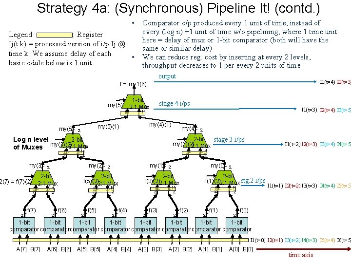
Strategy 4 a: (Synchronous) Pipeline It! (contd. ) • Legend : Register Ij(t k) = processed version of i/p Ij @ time k. We assume delay of each • basic odule below is 1 unit. Comparator o/p produced every 1 unit of time, instead of every (log n) +1 unit of time w/o pipelining, where 1 time unit here = delay of mux or 1 -bit comparator (both will have the same or similar delay) We can reduce reg. cost by inserting at every 2 levels, throughput decreases to 1 per every 2 units of time output I 1(t=4) I 2(t=5) F= my 1(6) 1 -bit my(5)(2)2: 1 Mux I 0 my(5) I 1(t=3) I 2(t=4) I 3(t=5) I 1 my(4)(1) my(5)(1) 2 stage 4 i/ps 2 -bit Log n level my(3)(2) 2: 1 Mux of Muxes I 1 I 0 2 my(3) I 0 2 2 f(7) I 0 2 my(2) I 1 2 I 0 2 f(6) my(1) 2 2 -bit f(5)(2)2: 1 Mux 2 2 -bit stage 3 i/ps my(1)(2) 2: 1 Mux 2 2 2 -bit 2(7) = f(7)(2) 2: 1 Mux my(4) f(5) I 1 I 0 2 2 2 f(4) 2 f(3) I 1 2 my(0) 2 2 -bit f(3)(2)2: 1 Mux I 1 2 f(2) 2 2 -bit f(1)(2)2: 1 Mux stg. 2 i/ps I 1(t=1) I 2(t=2) I 3(t=3) I 4(t=4) I 5(t=5) I 1 I 0 2 2 I 1(t=2) I 2(t=3) I 3(t=4) I 4(t=5) 2 f(1) 2 2 f(0) 1 -bit 1 -bit comparatorcomparator I 1(t=0) I 2(t=1) I 3(t=2) I 4(t=3) I 5(t=4) I 6(t=5) A[7] B[7] A[6] B[6] A[5] B[5] A[4] B[4] A[3] B[3] A[2] B[2] A[1] B[1] A[0] B[0] time axis

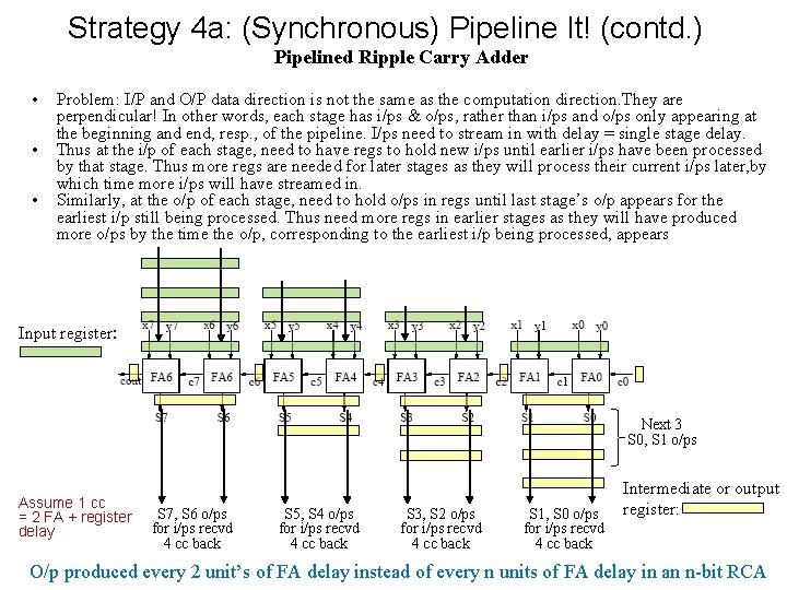
Strategy 4 a: (Synchronous) Pipeline It! (contd. ) Pipelined Ripple Carry Adder • • • Problem: I/P and O/P data direction is not the same as the computation direction. They are perpendicular! In other words, each stage has i/ps & o/ps, rather than i/ps and o/ps only appearing at the beginning and end, resp. , of the pipeline. I/ps need to stream in with delay = single stage delay. Thus at the i/p of each stage, need to have regs to hold new i/ps until earlier i/ps have been processed by that stage. Thus more regs are needed for later stages as they will process their current i/ps later, by which time more i/ps will have streamed in. Similarly, at the o/p of each stage, need to hold o/ps in regs until last stage’s o/p appears for the earliest i/p still being processed. Thus need more regs in earlier stages as they will have produced more o/ps by the time the o/p, corresponding to the earliest i/p being processed, appears Input register: Next 3 S 0, S 1 o/ps Assume 1 cc = 2 FA + register delay S 7, S 6 o/ps for i/ps recvd 4 cc back S 5, S 4 o/ps for i/ps recvd 4 cc back S 3, S 2 o/ps for i/ps recvd 4 cc back S 1, S 0 o/ps for i/ps recvd 4 cc back Intermediate or output register: O/p produced every 2 unit’s of FA delay instead of every n units of FA delay in an n-bit RCA

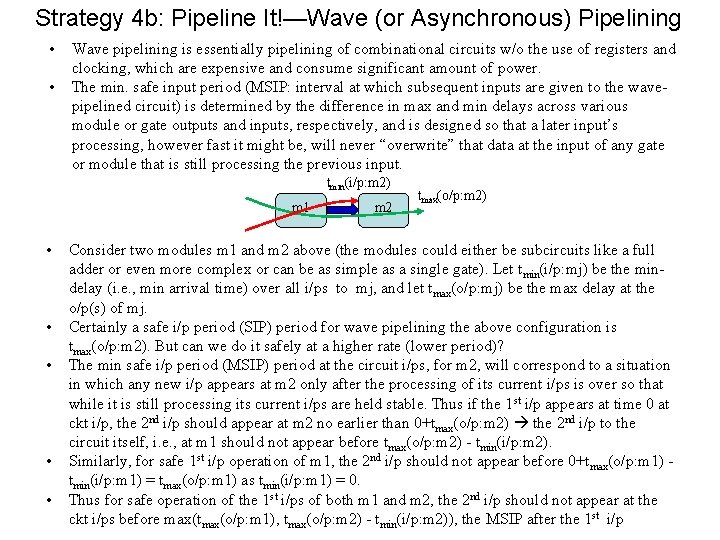
Strategy 4 b: Pipeline It!—Wave (or Asynchronous) Pipelining • • Wave pipelining is essentially pipelining of combinational circuits w/o the use of registers and clocking, which are expensive and consume significant amount of power. The min. safe input period (MSIP: interval at which subsequent inputs are given to the wavepipelined circuit) is determined by the difference in max and min delays across various module or gate outputs and inputs, respectively, and is designed so that a later input’s processing, however fast it might be, will never “overwrite” that data at the input of any gate or module that is still processing the previous input. tmin(i/p: m 2) m 1 • • • m 2 tmax(o/p: m 2) Consider two modules m 1 and m 2 above (the modules could either be subcircuits like a full adder or even more complex or can be as simple as a single gate). Let tmin(i/p: mj) be the mindelay (i. e. , min arrival time) over all i/ps to mj, and let tmax(o/p: mj) be the max delay at the o/p(s) of mj. Certainly a safe i/p period (SIP) period for wave pipelining the above configuration is tmax(o/p: m 2). But can we do it safely at a higher rate (lower period)? The min safe i/p period (MSIP) period at the circuit i/ps, for m 2, will correspond to a situation in which any new i/p appears at m 2 only after the processing of its current i/ps is over so that while it is still processing its current i/ps are held stable. Thus if the 1 st i/p appears at time 0 at ckt i/p, the 2 nd i/p should appear at m 2 no earlier than 0+tmax(o/p: m 2) the 2 nd i/p to the circuit itself, i. e. , at m 1 should not appear before tmax(o/p: m 2) - tmin(i/p: m 2). Similarly, for safe 1 st i/p operation of m 1, the 2 nd i/p should not appear before 0+tmax(o/p: m 1) tmin(i/p: m 1) = tmax(o/p: m 1) as tmin(i/p: m 1) = 0. Thus for safe operation of the 1 st i/ps of both m 1 and m 2, the 2 nd i/p should not appear at the ckt i/ps before max(tmax(o/p: m 1), tmax(o/p: m 2) - tmin(i/p: m 2)), the MSIP after the 1 st i/p

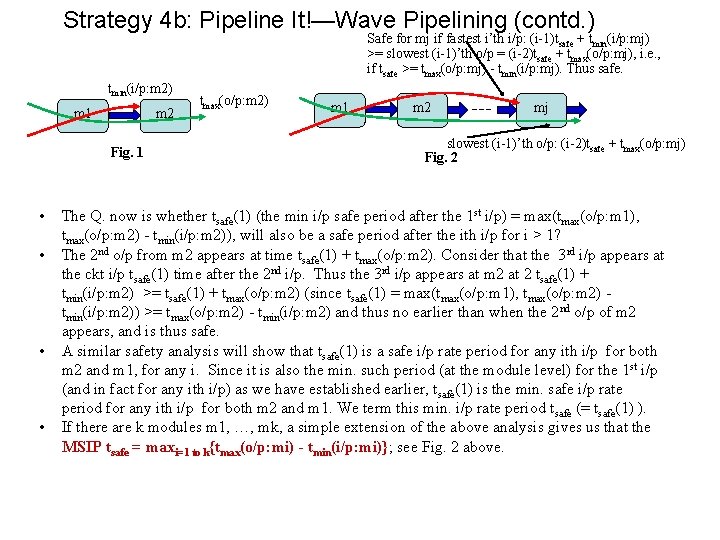
Strategy 4 b: Pipeline It!—Wave Pipelining (contd. ) Safe for mj if fastest i’th i/p: (i-1)tsafe + tmin(i/p: mj) >= slowest (i-1)’th o/p = (i-2)tsafe + tmax(o/p: mj), i. e. , if tsafe >= tmax(o/p: mj) - tmin(i/p: mj). Thus safe. tmin(i/p: m 2) m 1 m 2 Fig. 1 • • tmax(o/p: m 2) m 1 m 2 mj slowest (i-1)’th o/p: (i-2)tsafe + tmax(o/p: mj) Fig. 2 The Q. now is whether tsafe(1) (the min i/p safe period after the 1 st i/p) = max(tmax(o/p: m 1), tmax(o/p: m 2) - tmin(i/p: m 2)), will also be a safe period after the ith i/p for i > 1? The 2 nd o/p from m 2 appears at time tsafe(1) + tmax(o/p: m 2). Consider that the 3 rd i/p appears at the ckt i/p tsafe(1) time after the 2 nd i/p. Thus the 3 rd i/p appears at m 2 at 2 tsafe(1) + tmin(i/p: m 2) >= tsafe(1) + tmax(o/p: m 2) (since tsafe(1) = max(tmax(o/p: m 1), tmax(o/p: m 2) tmin(i/p: m 2)) >= tmax(o/p: m 2) - tmin(i/p: m 2) and thus no earlier than when the 2 nd o/p of m 2 appears, and is thus safe. A similar safety analysis will show that tsafe(1) is a safe i/p rate period for any ith i/p for both m 2 and m 1, for any i. Since it is also the min. such period (at the module level) for the 1 st i/p (and in fact for any ith i/p) as we have established earlier, tsafe(1) is the min. safe i/p rate period for any ith i/p for both m 2 and m 1. We term this min. i/p rate period tsafe (= tsafe(1) ). If there are k modules m 1, …, mk, a simple extension of the above analysis gives us that the MSIP tsafe = maxi=1 to k{tmax(o/p: mi) - tmin(i/p: mi)}; see Fig. 2 above.

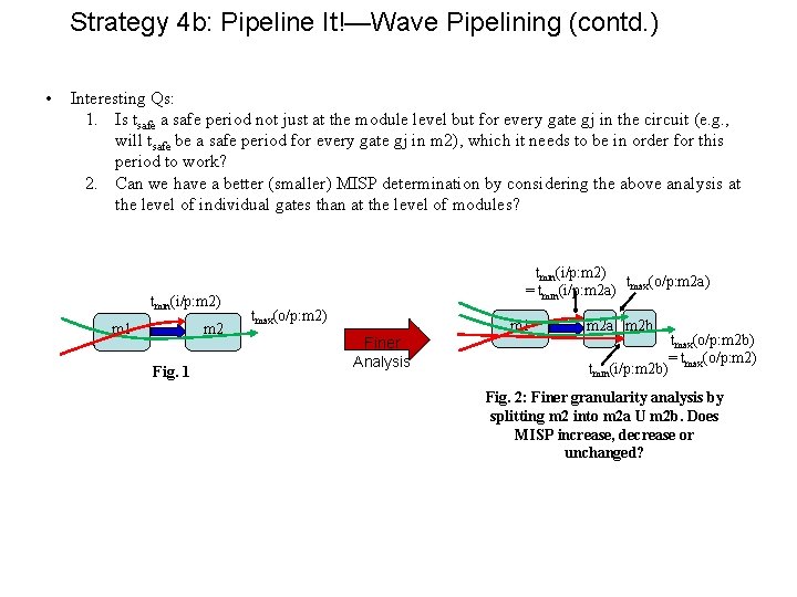
Strategy 4 b: Pipeline It!—Wave Pipelining (contd. ) • Interesting Qs: 1. Is tsafe a safe period not just at the module level but for every gate gj in the circuit (e. g. , will tsafe be a safe period for every gate gj in m 2), which it needs to be in order for this period to work? 2. Can we have a better (smaller) MISP determination by considering the above analysis at the level of individual gates than at the level of modules? tmin(i/p: m 2) m 1 m 2 Fig. 1 tmin(i/p: m 2) t (o/p: m 2 a) = tmin(i/p: m 2 a) max tmax(o/p: m 2) m 1 Finer Analysis m 2 a m 2 b tmin(i/p: m 2 b) tmax(o/p: m 2 b) = tmax(o/p: m 2) Fig. 2: Finer granularity analysis by splitting m 2 into m 2 a U m 2 b. Does MISP increase, decrease or unchanged?

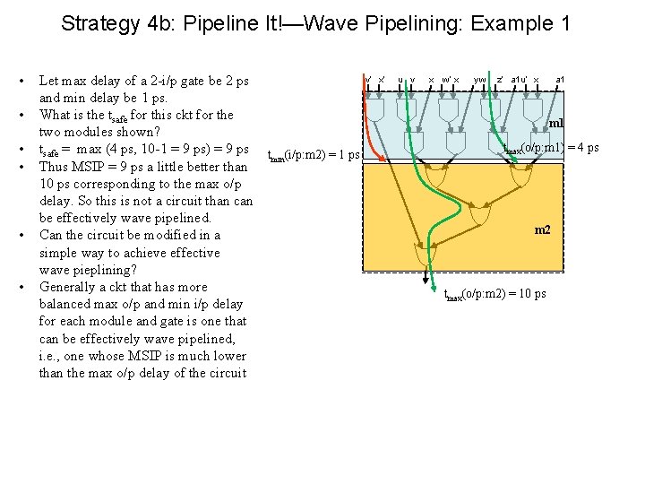
Strategy 4 b: Pipeline It!—Wave Pipelining: Example 1 • • • Let max delay of a 2 -i/p gate be 2 ps and min delay be 1 ps. What is the tsafe for this ckt for the two modules shown? tsafe = max (4 ps, 10 -1 = 9 ps) = 9 ps Thus MSIP = 9 ps a little better than 10 ps corresponding to the max o/p delay. So this is not a circuit than can be effectively wave pipelined. Can the circuit be modified in a simple way to achieve effective wave pieplining? Generally a ckt that has more balanced max o/p and min i/p delay for each module and gate is one that can be effectively wave pipelined, i. e. , one whose MSIP is much lower than the max o/p delay of the circuit v’ x’ u v x w’ x yw z’ a 1 u’ x a 1 m 1 tmin(i/p: m 2) = 1 ps tmax(o/p: m 1) = 4 ps m 2 tmax(o/p: m 2) = 10 ps

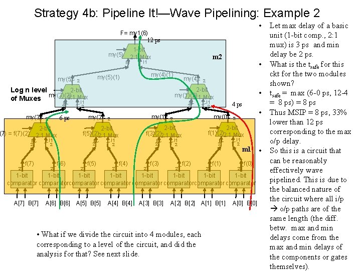
Strategy 4 b: Pipeline It!—Wave Pipelining: Example 2 • F= my 1(6) 12 ps 1 -bit my(5)(2)2: 1 Mux I 0 my(5) my(4)(1) my(5)(1) 2 m 2 I 1 2 -bit Log n level my(3)(2) 2: 1 Mux of Muxes I 1 I 0 2 my(3) 2 -bit (7) = f(7)(2) 2: 1 Mux I 1 I 0 2 2 f(7) 2 I 0 2 my(2) I 0 2 f(6) my(1) 2 2 -bit f(5)(2)2: 1 Mux 2 2 -bit my(1)(2) 2: 1 Mux 2 6 ps 2 my(4) • f(5) I 1 I 0 2 2 f(4) 2 f(3) I 1 4 ps 2 my(0) 2 2 -bit f(3)(2)2: 1 Mux 2 • I 1 2 -bit f(1)(2)2: 1 Mux I 0 2 2 2 f(2) • 2 2 f(1) I 1 2 2 m 1 f(0) 1 -bit 1 -bit comparatorcomparator A[7] B[7] A[6] B[6] A[5] B[5] A[4] B[4] A[3] B[3] A[2] B[2] A[1] B[1] • What if we divide the circuit into 4 modules, each corresponding to a level of the circuit, and did the analysis for that? See next slide. A[0] B[0] • Let max delay of a basic unit (1 -bit comp. , 2: 1 mux) is 3 ps and min delay be 2 ps. What is the tsafe for this ckt for the two modules shown? tsafe = max (6 -0 ps, 12 -4 = 8 ps) = 8 ps Thus MSIP = 8 ps, 33% lower than 12 ps corresponding to the max o/p delay. So this is a circuit that can be reasonably effectively wave pipelined. This is due to the balanced nature of the circuit where all i/p o/p paths are of the same length (the diff. betw. max and min delays come from the max and min delays of the components or gates themselves).

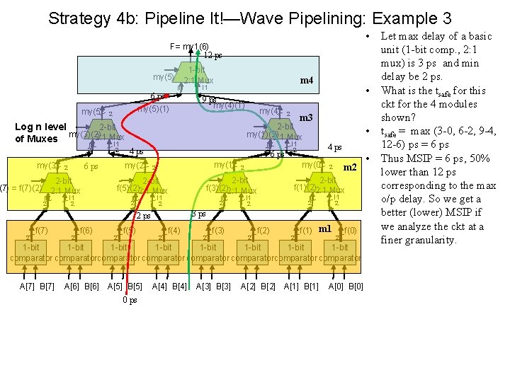
Strategy 4 b: Pipeline It!—Wave Pipelining: Example 3 • F= my 1(6) 12 ps 1 -bit my(5)(2)2: 1 Mux I 0 6 ps my(5)(1) 2 2 -bit Log n level my(3)(2) 2: 1 Mux of Muxes I 1 I 0 2 my(3) I 0 I 1 I 0 2 my(1) 2 I 0 2 I 1 f(7) 2 f(6) 2 2 • m 3 f(5) I 0 2 6 ps • I 1 4 ps 2 my(0) 2 2 -bit f(3)(2)2: 1 Mux 2 I 1 m 2 2 2 -bit f(1)(2)2: 1 Mux I 1 I 0 2 2 2 3 ps 2 my(4) 4 ps 2 -bit f(5)(2)2: 1 Mux 2 9 ps my(4)(1) 2 -bit my(1)(2) 2: 1 Mux my(2) 6 ps 2 2 -bit (7) = f(7)(2) 2: 1 Mux 2 2 m 4 I 1 2 f(4) 2 f(3) 2 f(2) 2 f(1) m 1 2 f(0) 1 -bit 1 -bit comparatorcomparator A[7] B[7] A[6] B[6] A[5] B[5] 0 ps A[4] B[4] A[3] B[3] A[2] B[2] A[1] B[1] A[0] B[0] • Let max delay of a basic unit (1 -bit comp. , 2: 1 mux) is 3 ps and min delay be 2 ps. What is the tsafe for this ckt for the 4 modules shown? tsafe = max (3 -0, 6 -2, 9 -4, 12 -6) ps = 6 ps Thus MSIP = 6 ps, 50% lower than 12 ps corresponding to the max o/p delay. So we get a better (lower) MSIP if we analyze the ckt at a finer granularity.

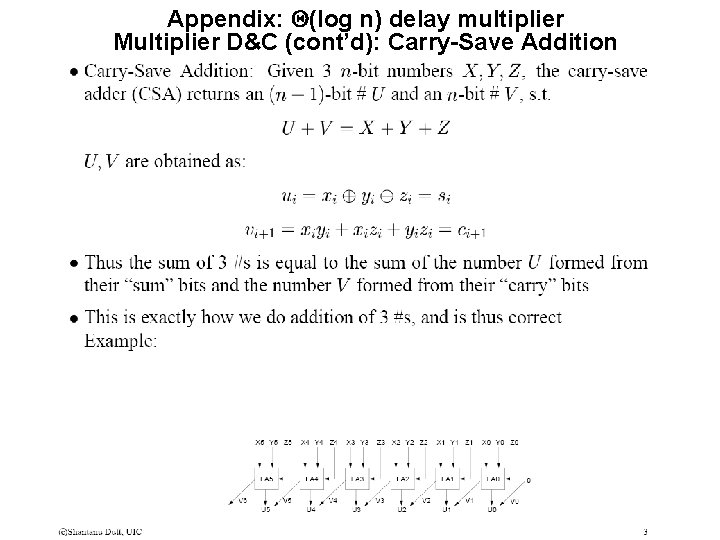
Appendix: Q(log n) delay multiplier Multiplier D&C (cont’d): Carry-Save Addition

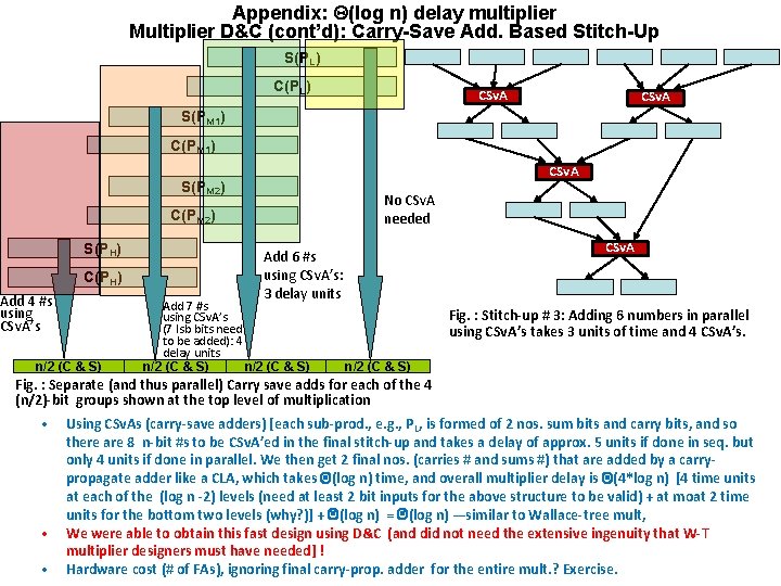
Appendix: Q(log n) delay multiplier Multiplier D&C (cont’d): Carry-Save Add. Based Stitch-Up S(PL) CSv. A S(PM 1) CSv. A S(PM 2) No CSv. A needed C(PM 2) S(PH) C(PH) Add 4 #s using CSv. A’s n/2 (C & S) CSv. A Add 6 #s using CSv. A’s: 3 delay units Add 7 #s using CSv. A’s (7 lsb bits need to be added): 4 delay units n/2 (C & S) Fig. : Stitch-up # 3: Adding 6 numbers in parallel using CSv. A’s takes 3 units of time and 4 CSv. A’s. n/2 (C & S) Fig. : Separate (and thus parallel) Carry save adds for each of the 4 (n/2)-bit groups shown at the top level of multiplication • • • Using CSv. As (carry-save adders) [each sub-prod. , e. g. , PL, is formed of 2 nos. sum bits and carry bits, and so there are 8 n-bit #s to be CSv. A’ed in the final stitch-up and takes a delay of approx. 5 units if done in seq. but only 4 units if done in parallel. We then get 2 final nos. (carries # and sums #) that are added by a carrypropagate adder like a CLA, which takes Q(log n) time, and overall multiplier delay is Q(4*log n) [4 time units at each of the (log n -2) levels (need at least 2 bit inputs for the above structure to be valid) + at moat 2 time units for the bottom two levels (why? )] + Q(log n) = Q(log n) —similar to Wallace-tree mult, We were able to obtain this fast design using D&C (and did not need the extensive ingenuity that W-T multiplier designers must have needed] ! Hardware cost (# of FAs), ignoring final carry-prop. adder for the entire mult. ? Exercise.