DNT 2363 MATERIAL ENGINEERING SEMESTER 1 20152016 CHAPTER



- Slides: 45

DNT 236/3 MATERIAL ENGINEERING SEMESTER 1 – 2015/2016

CHAPTER 3 Solidification and Crystalline Imperfection 2

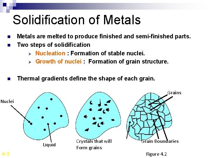
Solidification of Metals n n n Metals are melted to produce finished and semi-finished parts. Two steps of solidification Ø Nucleation : Formation of stable nuclei. Ø Growth of nuclei : Formation of grain structure. Thermal gradients define the shape of each grain. Grains Nuclei Liquid 4 -2 Crystals that will Form grains Grain Boundaries Figure 4. 2

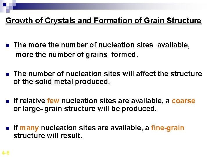
Growth of Crystals and Formation of Grain Structure n Nucleus grow into crystals in different orientations. n Crystal boundaries are formed when crystals join together at complete solidification. n Crystals in solidified metals are called grains. n Grains are separated by grain boundaries. 4 -8

Growth of Crystals and Formation of Grain Structure n The more the number of nucleation sites available, more the number of grains formed. n The number of nucleation sites will affect the structure of the solid metal produced. n If relative few nucleation sites are available, a coarse or large- grain structure will be produced. n If many nucleation sites are available, a fine-grain structure will result. 4 -8

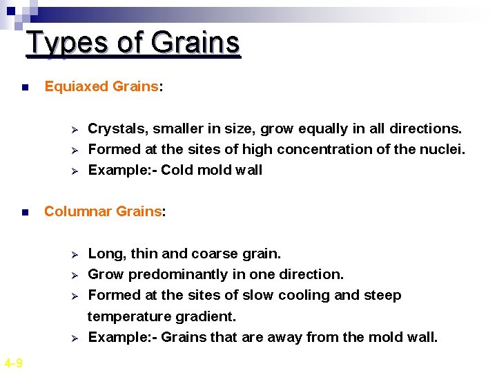
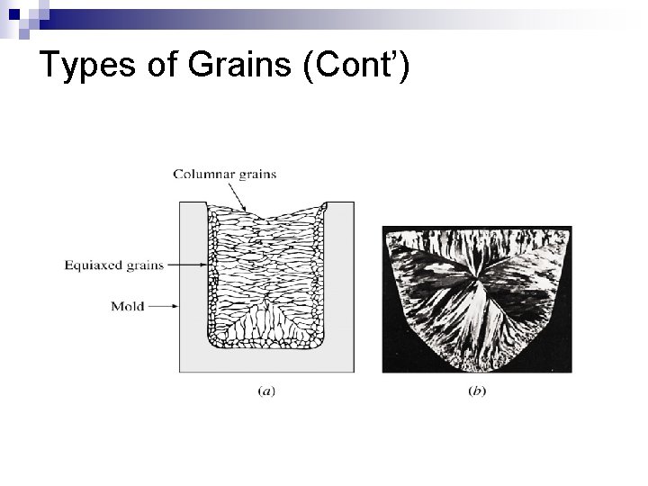
Types of Grains n Equiaxed Grains: Ø Ø Ø n Columnar Grains: Ø Ø 4 -9 Crystals, smaller in size, grow equally in all directions. Formed at the sites of high concentration of the nuclei. Example: - Cold mold wall Long, thin and coarse grain. Grow predominantly in one direction. Formed at the sites of slow cooling and steep temperature gradient. Example: - Grains that are away from the mold wall.

Types of Grains (Cont’)

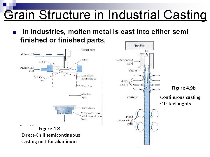
Grain Structure in Industrial Casting n In industries, molten metal is cast into either semi finished or finished parts. Figure 4. 9 b Continuous casting Of steel ingots Figure 4. 8 Direct-Chill semicontinuous Casting unit for aluminum

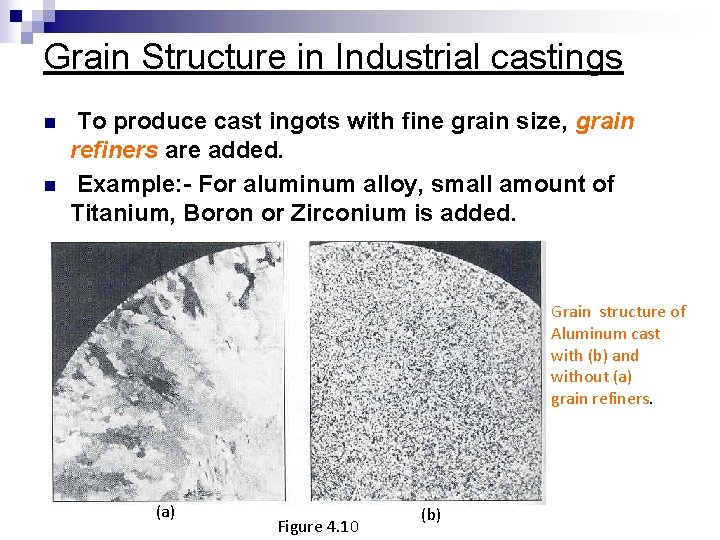
Grain Structure in Industrial castings n n To produce cast ingots with fine grain size, grain refiners are added. Example: - For aluminum alloy, small amount of Titanium, Boron or Zirconium is added. Grain structure of Aluminum cast with (b) and without (a) grain refiners. (a) Figure 4. 10 (b)

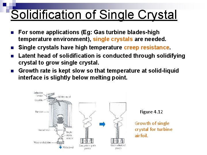
Solidification of Single Crystal n n For some applications (Eg: Gas turbine blades-high temperature environment), single crystals are needed. Single crystals have high temperature creep resistance. Latent head of solidification is conducted through solidifying crystal to grow single crystal. Growth rate is kept slow so that temperature at solid-liquid interface is slightly below melting point. Figure 4. 12 Growth of single crystal for turbine airfoil.

Solidification of Single Crystal n n n 4 -13 Silicon single crystal is another example of industrial use of single crystal. Silicon single crystals are sliced into wafers for solid-state electronic integrated circuit chips. Single crystals are necessary for this application since grain boundaries would disrupt the flow of electrons in the device made from semiconductor silicon.

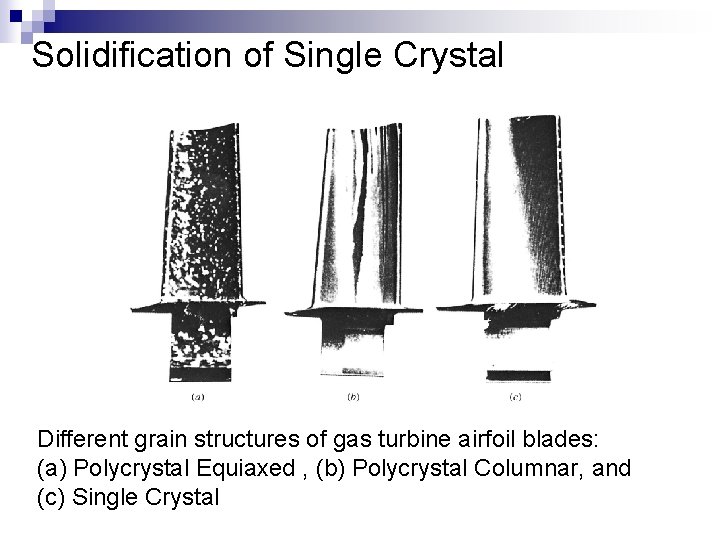
Solidification of Single Crystal Different grain structures of gas turbine airfoil blades: (a) Polycrystal Equiaxed , (b) Polycrystal Columnar, and (c) Single Crystal

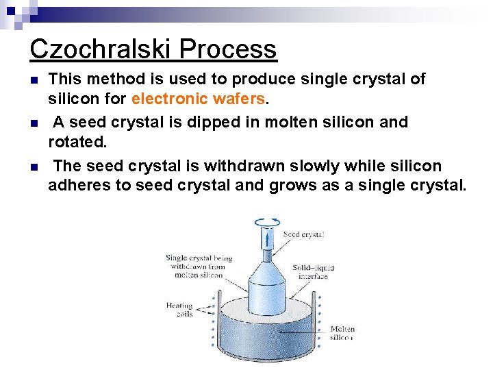
Czochralski Process n n n This method is used to produce single crystal of silicon for electronic wafers. A seed crystal is dipped in molten silicon and rotated. The seed crystal is withdrawn slowly while silicon adheres to seed crystal and grows as a single crystal.

Metallic Solid Solutions n n n Few metals that are used in pure or nearly pure state are like high purity copper in electronic wire and high-purity aluminum used for bright metallic surface. Alloys are used in most engineering applications. Alloy is an mixture of two or more metals and nonmetals. Example: Ø Cartridge brass is binary alloy of 70% Cu and 30% Zinc. Ø Iconel is a nickel based superalloy with about 10 elements. Solid solution is a simple type of alloy in which elements are dispersed in a single phase. There are two types of solid solutions: substitutional and interstitial

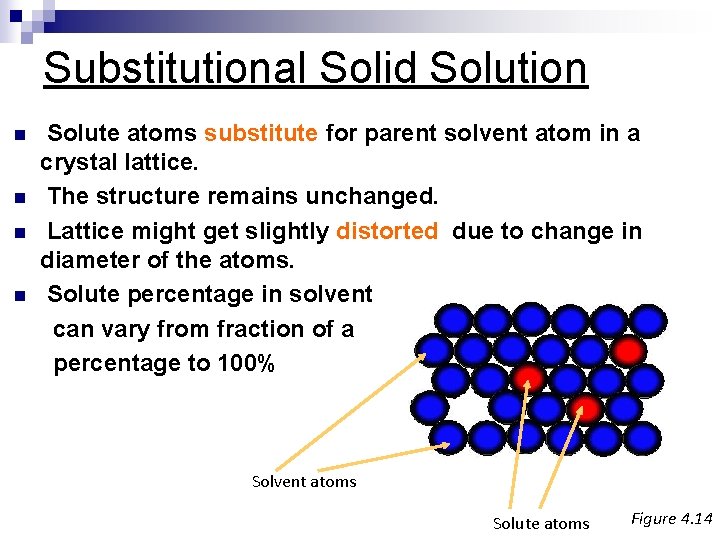
Substitutional Solid Solution n n Solute atoms substitute for parent solvent atom in a crystal lattice. The structure remains unchanged. Lattice might get slightly distorted due to change in diameter of the atoms. Solute percentage in solvent can vary from fraction of a percentage to 100% Solvent atoms Solute atoms Figure 4. 14

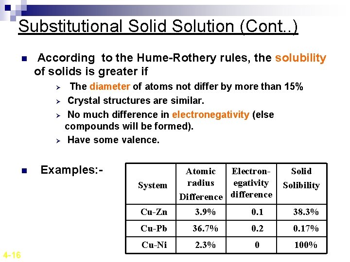
Substitutional Solid Solution (Cont. . ) n According to the Hume-Rothery rules, the solubility of solids is greater if Ø Ø n The diameter of atoms not differ by more than 15% Crystal structures are similar. No much difference in electronegativity (else compounds will be formed). Have some valence. Examples: System 4 -16 Atomic Electronradius egativity Difference difference Solid Solibility Cu-Zn 3. 9% 0. 1 38. 3% Cu-Pb 36. 7% 0. 2 0. 17% Cu-Ni 2. 3% 0 100%

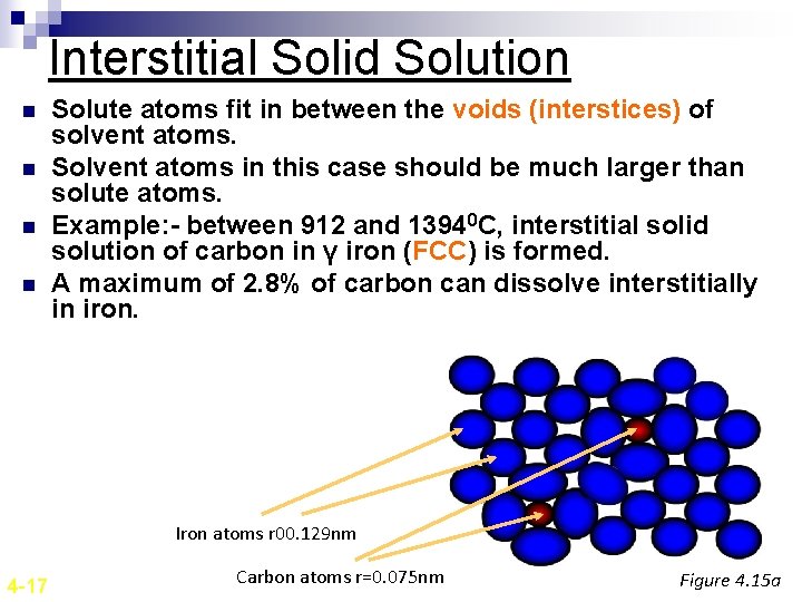
Interstitial Solid Solution n n Solute atoms fit in between the voids (interstices) of solvent atoms. Solvent atoms in this case should be much larger than solute atoms. Example: - between 912 and 13940 C, interstitial solid solution of carbon in γ iron (FCC) is formed. A maximum of 2. 8% of carbon can dissolve interstitially in iron. Iron atoms r 00. 129 nm 4 -17 Carbon atoms r=0. 075 nm Figure 4. 15 a

Crystalline Imperfections n n n 4 -18 No crystal is perfect. Imperfections affect mechanical properties, chemical properties and electrical properties. Imperfections can be classified as Ø Zero dimension /point defects. Ø One dimension / line defects (dislocations). Ø Two dimension defects. Ø Three dimension defects (cracks).

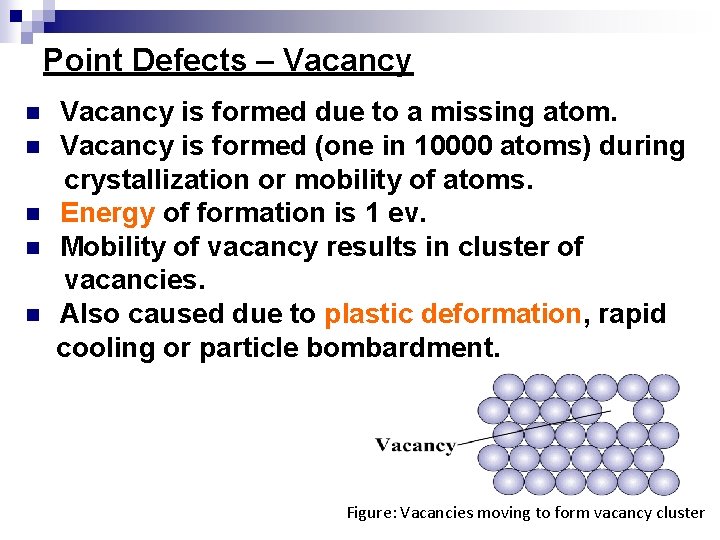
Point Defects – Vacancy n n n Vacancy is formed due to a missing atom. Vacancy is formed (one in 10000 atoms) during crystallization or mobility of atoms. Energy of formation is 1 ev. Mobility of vacancy results in cluster of vacancies. Also caused due to plastic deformation, rapid cooling or particle bombardment. Figure: Vacancies moving to form vacancy cluster

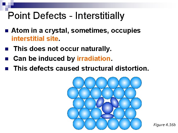
Point Defects - Interstitially n n Atom in a crystal, sometimes, occupies interstitial site. This does not occur naturally. Can be induced by irradiation. This defects caused structural distortion. Figure 4. 16 b

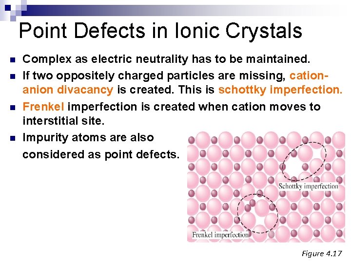
Point Defects in Ionic Crystals n n Complex as electric neutrality has to be maintained. If two oppositely charged particles are missing, cationanion divacancy is created. This is schottky imperfection. Frenkel imperfection is created when cation moves to interstitial site. Impurity atoms are also considered as point defects. Figure 4. 17

Line Defects – (Dislocations) n Lattice distortions are centered around a line. n Formed during Ø Solidification Ø Permanent Deformation Ø Vacancy condensation n Different types of line defects are Ø Edge dislocation Ø Screw dislocation Ø Mixed dislocation

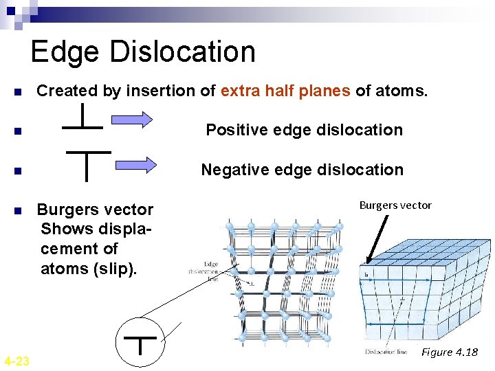
Edge Dislocation n Created by insertion of extra half planes of atoms. n Positive edge dislocation n Negative edge dislocation n 4 -23 Burgers vector Shows displacement of atoms (slip). Burgers vector Figure 4. 18

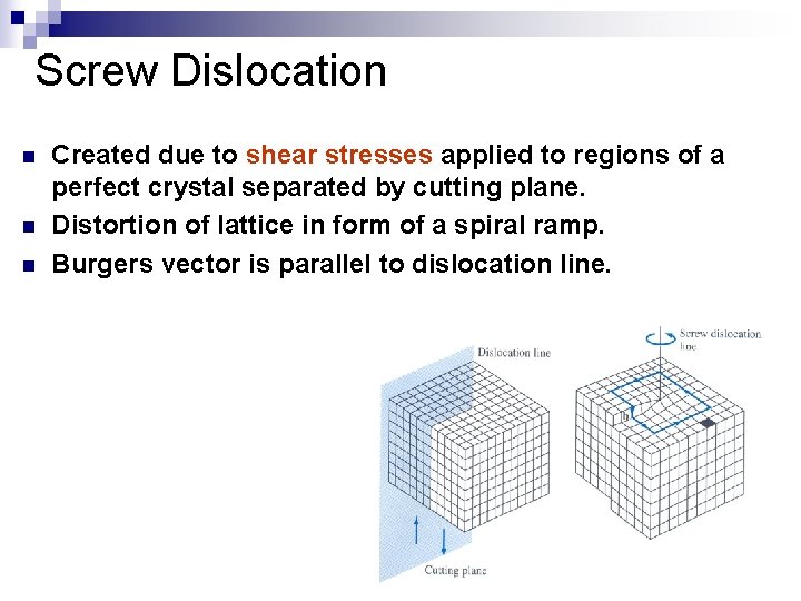
Screw Dislocation n Created due to shear stresses applied to regions of a perfect crystal separated by cutting plane. Distortion of lattice in form of a spiral ramp. Burgers vector is parallel to dislocation line.

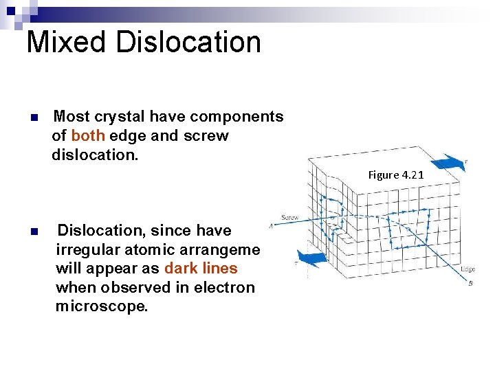
Mixed Dislocation n Most crystal have components of both edge and screw dislocation. Figure 4. 21 n Dislocation, since have irregular atomic arrangement will appear as dark lines when observed in electron microscope.

Planar Defects Grain boundaries, twins, low/high angle boundaries, twists and stacking faults n Free surface is also a defect : Bonded to atoms on only one side and hence has higher state of energy Highly reactive n Nanomaterials have small clusters of atoms and hence are highly reactive. n

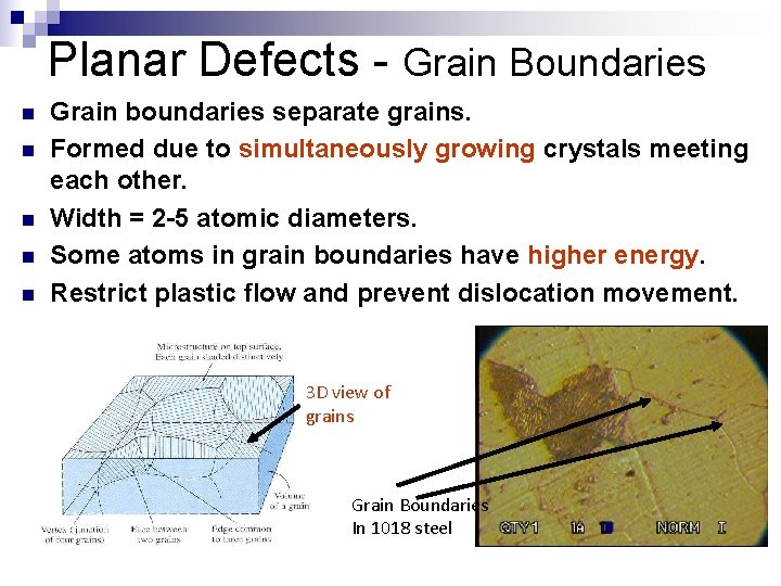
Planar Defects - Grain Boundaries n n n Grain boundaries separate grains. Formed due to simultaneously growing crystals meeting each other. Width = 2 -5 atomic diameters. Some atoms in grain boundaries have higher energy. Restrict plastic flow and prevent dislocation movement. 3 D view of grains Grain Boundaries In 1018 steel

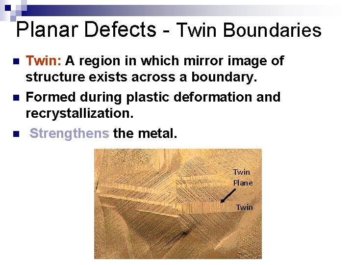
Planar Defects - Twin Boundaries n n n Twin: A region in which mirror image of structure exists across a boundary. Formed during plastic deformation and recrystallization. Strengthens the metal. Twin Plane Twin

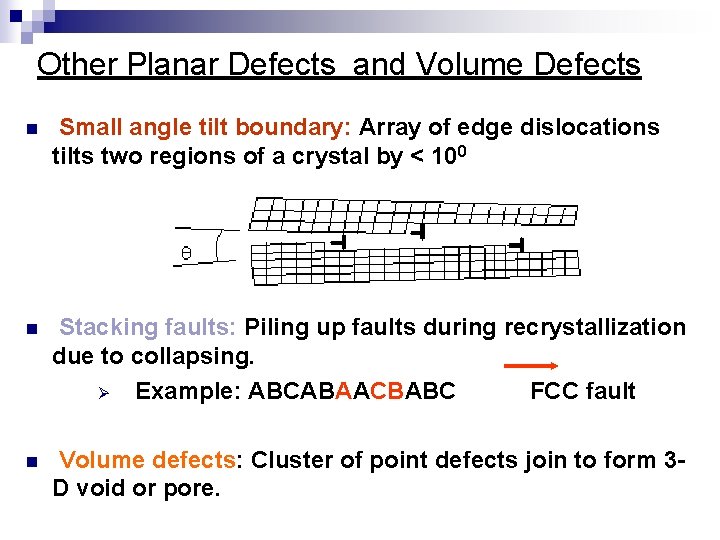
Other Planar Defects and Volume Defects n Small angle tilt boundary: Array of edge dislocations tilts two regions of a crystal by < 100 n Stacking faults: Piling up faults during recrystallization due to collapsing. Ø Example: ABCABAACBABC FCC fault n Volume defects: Cluster of point defects join to form 3 D void or pore.

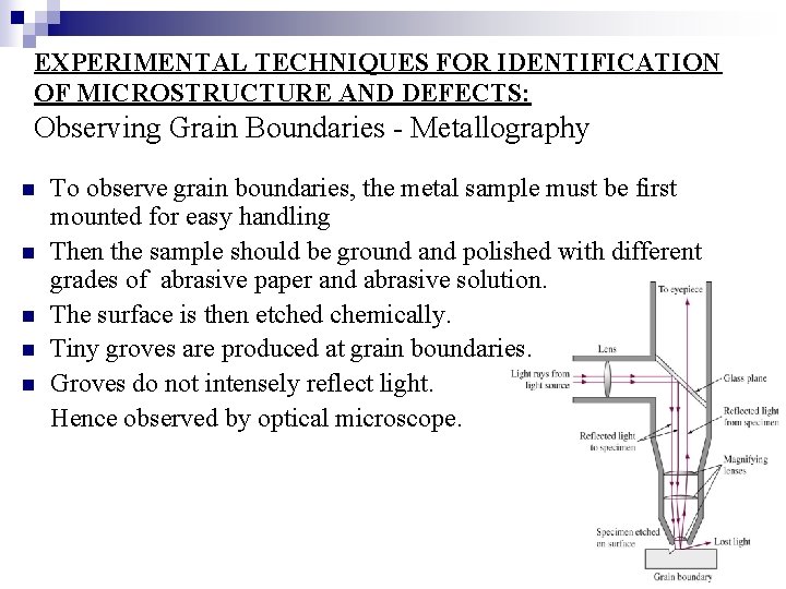
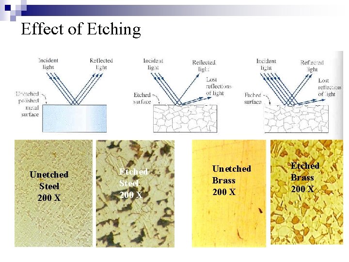
EXPERIMENTAL TECHNIQUES FOR IDENTIFICATION OF MICROSTRUCTURE AND DEFECTS: Observing Grain Boundaries - Metallography n n n To observe grain boundaries, the metal sample must be first mounted for easy handling Then the sample should be ground and polished with different grades of abrasive paper and abrasive solution. The surface is then etched chemically. Tiny groves are produced at grain boundaries. Groves do not intensely reflect light. Hence observed by optical microscope.

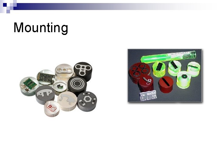
Sample preparation Mounting Grinding Etching Polishing

Mounting


Sectioning, Cutting and polishing

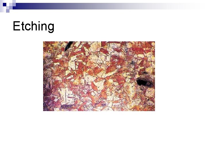
Etching

Effect of Etching Unetched Steel 200 X Etched Steel 200 X Unetched Brass 200 X Etched Brass 200 X

Grain Size Affects the mechanical properties of the material n The smaller the grain size, more are the grain boundaries. n More grain boundaries means higher resistance to slip (plastic deformation occurs due to slip). n More grains means more uniform the mechanical properties are. n 37

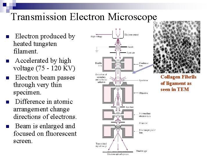
Transmission Electron Microscope n n n Electron produced by heated tungsten filament. Accelerated by high voltage (75 - 120 KV) Electron beam passes through very thin specimen. Difference in atomic arrangement change directions of electrons. Beam is enlarged and focused on fluorescent screen. Collagen Fibrils of ligament as seen in TEM

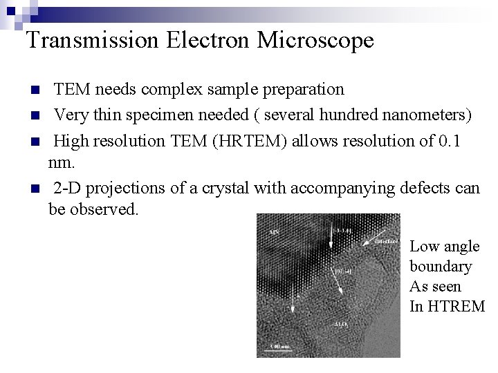
Transmission Electron Microscope n n TEM needs complex sample preparation Very thin specimen needed ( several hundred nanometers) High resolution TEM (HRTEM) allows resolution of 0. 1 nm. 2 -D projections of a crystal with accompanying defects can be observed. Low angle boundary As seen In HTREM

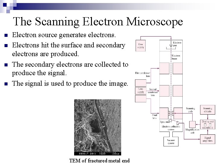
The Scanning Electron Microscope n n Electron source generates electrons. Electrons hit the surface and secondary electrons are produced. The secondary electrons are collected to produce the signal. The signal is used to produce the image. TEM of fractured metal end

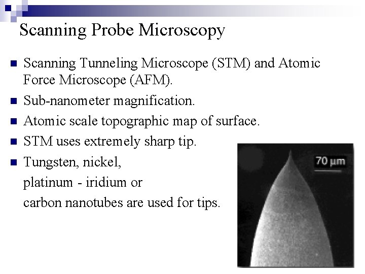
Scanning Probe Microscopy n n n Scanning Tunneling Microscope (STM) and Atomic Force Microscope (AFM). Sub-nanometer magnification. Atomic scale topographic map of surface. STM uses extremely sharp tip. Tungsten, nickel, platinum - iridium or carbon nanotubes are used for tips.

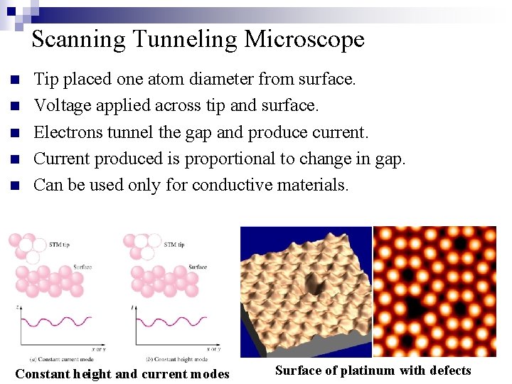
Scanning Tunneling Microscope n n n Tip placed one atom diameter from surface. Voltage applied across tip and surface. Electrons tunnel the gap and produce current. Current produced is proportional to change in gap. Can be used only for conductive materials. Constant height and current modes Surface of platinum with defects

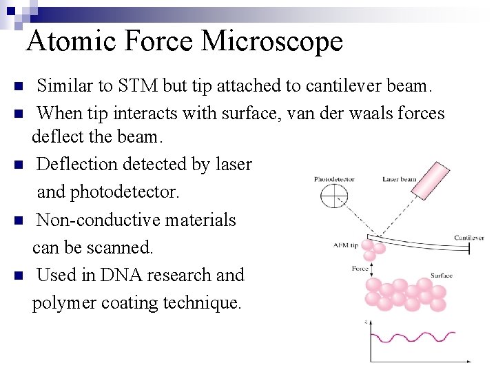
Atomic Force Microscope n n n Similar to STM but tip attached to cantilever beam. When tip interacts with surface, van der waals forces deflect the beam. Deflection detected by laser and photodetector. Non-conductive materials can be scanned. Used in DNA research and polymer coating technique.

n point defect – vacancy - iqbal - interstitially - hafizul – frenkel – asyraf – ABSENT – 1 GROUP - schottky – huzaifah burhanudin Line defect – diclocations – ameera - haziq azizan- ABSENT – 1 GROUP Planar defect – grain boundaries - zakuan - twin boundaries - fahman

ASSIGNMENT 2 Point defect – vacancy - interstitially – frenkel - schottky Line defect – dislocations Planar defect – grain boundaries - twin boundaries