DNT 2363 ENGINEERING MATERIALS SEMESTER 1 20182019 CHAPTER




- Slides: 39

DNT 236/3 ENGINEERING MATERIALS SEMESTER 1 – 2018/2019

CHAPTER 3 Solidification and Crystalline Imperfection 2

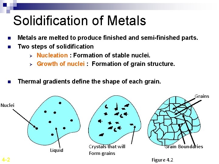
Solidification of Metals n n n Metals are melted to produce finished and semi-finished parts. Two steps of solidification Ø Nucleation : Formation of stable nuclei. Ø Growth of nuclei : Formation of grain structure. Thermal gradients define the shape of each grain. Grains Nuclei Liquid 4 -2 Crystals that will Form grains Grain Boundaries Figure 4. 2

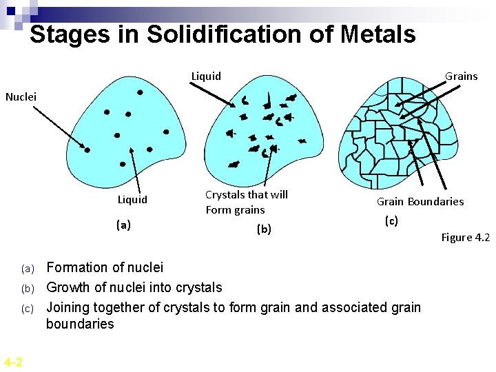
Stages in Solidification of Metals Liquid Grains Nuclei Liquid (a) (b) (c) 4 -2 Crystals that will Form grains (b) Grain Boundaries (c) Formation of nuclei Growth of nuclei into crystals Joining together of crystals to form grain and associated grain boundaries Figure 4. 2

Growth of Crystals in Liquid Metal and Formation of a Grain Structure n Nucleus grow into crystals in different orientations. n Crystal boundaries are formed when crystals join together at complete solidification. n Crystals in solidified metals are called grains. n Grains are separated by grain boundaries. 4 -8

Growth of Crystals in Liquid Metal and Formation of a Grain Structure n The more the number of nucleation sites available, more the number of grains formed. n The number of nucleation sites will affect the structure of the solid metal produced. n If relative few nucleation sites are available, a coarse or large-grain structure will be produced. n If many nucleation sites are available, a fine-grain structure will result. n Almost all engineering metals and alloy are cast with a fine-grain structure since this is the most desirable type for strength and uniformity of finished metal products. 4 -8

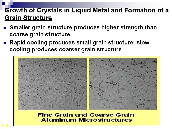
Growth of Crystals in Liquid Metal and Formation of a Grain Structure n n 4 -8 Smaller grain structure produces higher strength than coarse grain structure Rapid cooling produces small grain structure; slow cooling produces coarser grain structure

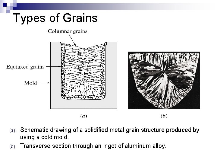
Types of Grains n When a pure metal is cast into a stationary mold without the use of grain refiners (a material added to a molten metal to attain finer grains in the final grain structure), two major types of grain structures are usually produced: ¨ Equiaxed Ø Ø Ø ¨ Crystals, smaller in size, grow equally in all directions. Formed at the sites of high concentration of the nuclei. Example: - Cold mold wall Columnar Grains: Ø Ø 4 -9 Grains: Long, thin and coarse grain. Grow predominantly in one direction. Formed at the sites of slow cooling and steep temperature gradient. Example: - Grains that are away from the mold wall.

Types of Grains (a) (b) Schematic drawing of a solidified metal grain structure produced by using a cold mold. Transverse section through an ingot of aluminum alloy.

Grain Size Affects the mechanical properties of the material n The smaller the grain size, more are the grain boundaries. n More grain boundaries means higher resistance to slip (plastic deformation occurs due to slip). n More grains means more uniform the mechanical properties are. n

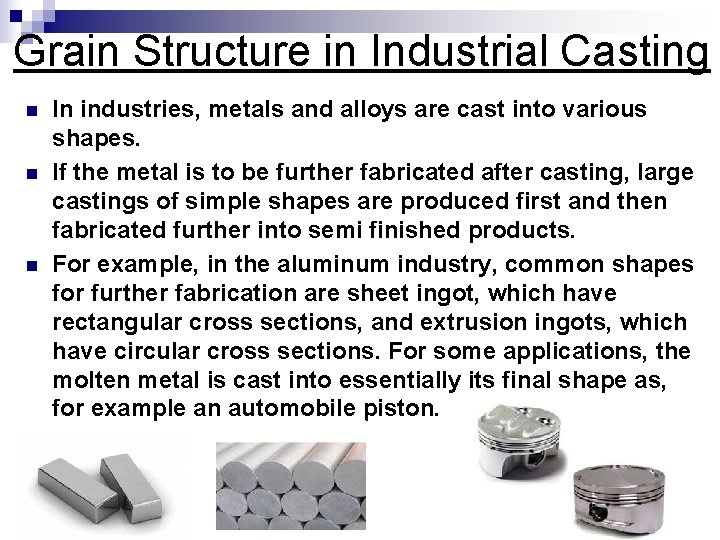
Grain Structure in Industrial Casting n n n In industries, metals and alloys are cast into various shapes. If the metal is to be further fabricated after casting, large castings of simple shapes are produced first and then fabricated further into semi finished products. For example, in the aluminum industry, common shapes for further fabrication are sheet ingot, which have rectangular cross sections, and extrusion ingots, which have circular cross sections. For some applications, the molten metal is cast into essentially its final shape as, for example an automobile piston.

Grain Structure in Industrial Casting Figure 4. 9 b Continuous casting Of steel ingots Figure 4. 8 Direct-Chill semicontinuous Casting unit for aluminum

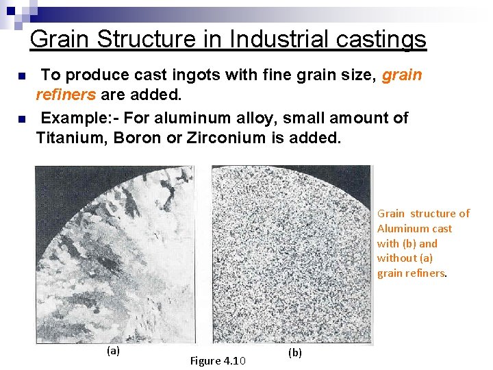
Grain Structure in Industrial castings n n To produce cast ingots with fine grain size, grain refiners are added. Example: - For aluminum alloy, small amount of Titanium, Boron or Zirconium is added. Grain structure of Aluminum cast with (b) and without (a) grain refiners. (a) Figure 4. 10 (b)

Crystalline Imperfections n n n 4 -18 No crystal is perfect. Imperfections affect many of crystals physical and mechanical properties, which in turn affect many important engineering properties of materials such as the cold formability of alloys, the electronic conductivity of semiconductors, the rate of migration of atoms in alloys and the corrosion on metals. Imperfections can be classified as Ø Zero dimension /point defects. Ø One dimension / line defects (dislocations). Ø Two dimension defects. Ø Three dimension defects (cracks).

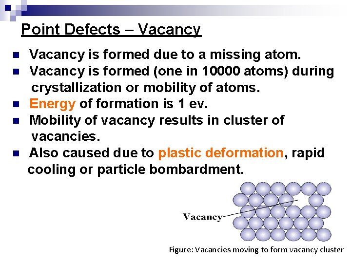
Point Defects – Vacancy n n n Vacancy is formed due to a missing atom. Vacancy is formed (one in 10000 atoms) during crystallization or mobility of atoms. Energy of formation is 1 ev. Mobility of vacancy results in cluster of vacancies. Also caused due to plastic deformation, rapid cooling or particle bombardment. Figure: Vacancies moving to form vacancy cluster

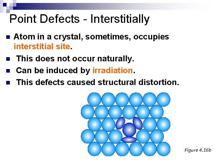
Point Defects - Interstitially n n Atom in a crystal, sometimes, occupies interstitial site. This does not occur naturally. Can be induced by irradiation. This defects caused structural distortion. Figure 4. 16 b

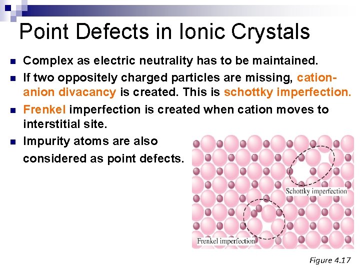
Point Defects in Ionic Crystals n n Complex as electric neutrality has to be maintained. If two oppositely charged particles are missing, cationanion divacancy is created. This is schottky imperfection. Frenkel imperfection is created when cation moves to interstitial site. Impurity atoms are also considered as point defects. Figure 4. 17

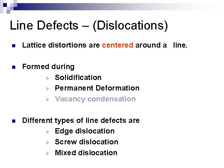
Line Defects – (Dislocations) n Lattice distortions are centered around a line. n Formed during Ø Solidification Ø Permanent Deformation Ø Vacancy condensation n Different types of line defects are Ø Edge dislocation Ø Screw dislocation Ø Mixed dislocation

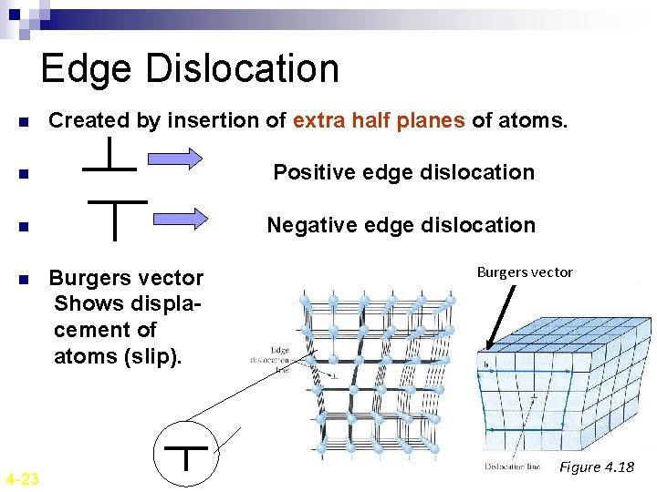
Edge Dislocation n Created by insertion of extra half planes of atoms. n Positive edge dislocation n Negative edge dislocation n 4 -23 Burgers vector Shows displacement of atoms (slip). Burgers vector Figure 4. 18

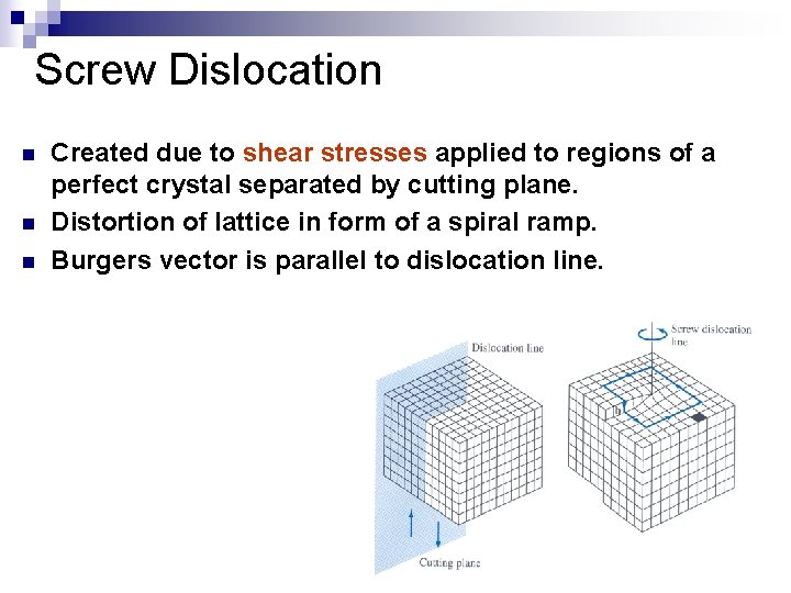
Screw Dislocation n Created due to shear stresses applied to regions of a perfect crystal separated by cutting plane. Distortion of lattice in form of a spiral ramp. Burgers vector is parallel to dislocation line.

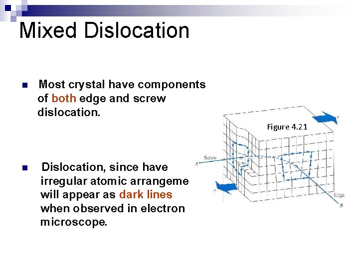
Mixed Dislocation n Most crystal have components of both edge and screw dislocation. Figure 4. 21 n Dislocation, since have irregular atomic arrangement will appear as dark lines when observed in electron microscope.

Planar Defects Grain boundaries, twins, low/high angle boundaries, twists and stacking faults n Free surface is also a defect : Bonded to atoms on only one side and hence has higher state of energy Highly reactive n Nanomaterials have small clusters of atoms and hence are highly reactive. n

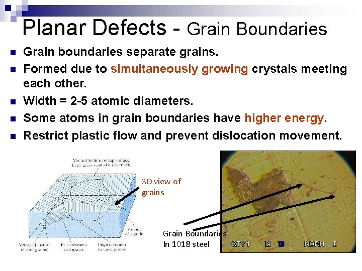
Planar Defects - Grain Boundaries n n n Grain boundaries separate grains. Formed due to simultaneously growing crystals meeting each other. Width = 2 -5 atomic diameters. Some atoms in grain boundaries have higher energy. Restrict plastic flow and prevent dislocation movement. 3 D view of grains Grain Boundaries In 1018 steel

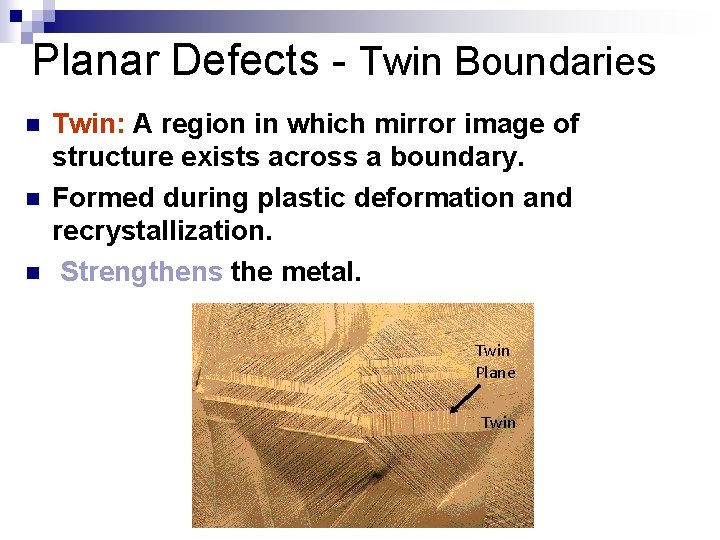
Planar Defects - Twin Boundaries n n n Twin: A region in which mirror image of structure exists across a boundary. Formed during plastic deformation and recrystallization. Strengthens the metal. Twin Plane Twin

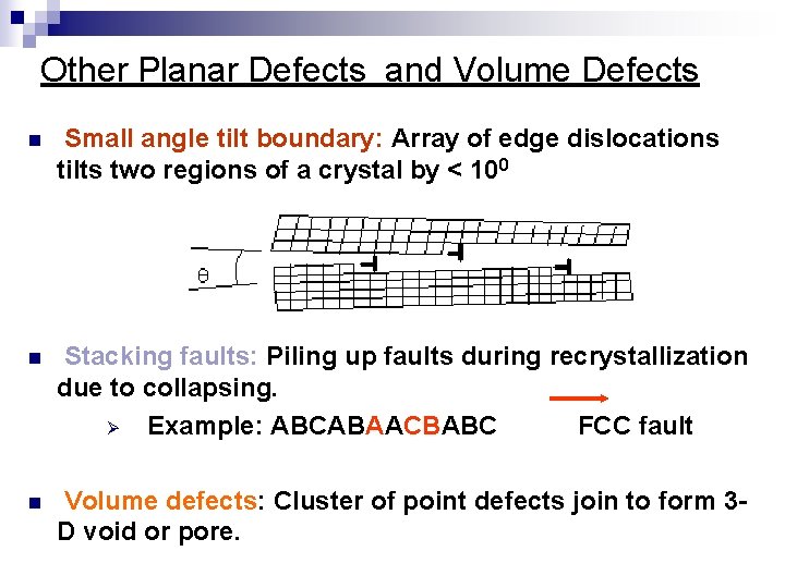
Other Planar Defects and Volume Defects n Small angle tilt boundary: Array of edge dislocations tilts two regions of a crystal by < 100 n Stacking faults: Piling up faults during recrystallization due to collapsing. Ø Example: ABCABAACBABC FCC fault n Volume defects: Cluster of point defects join to form 3 D void or pore.

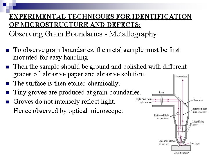
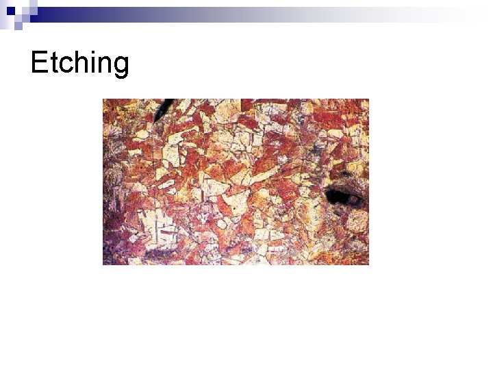
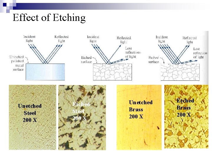
EXPERIMENTAL TECHNIQUES FOR IDENTIFICATION OF MICROSTRUCTURE AND DEFECTS: Observing Grain Boundaries - Metallography n n n To observe grain boundaries, the metal sample must be first mounted for easy handling Then the sample should be ground and polished with different grades of abrasive paper and abrasive solution. The surface is then etched chemically. Tiny groves are produced at grain boundaries. Groves do not intensely reflect light. Hence observed by optical microscope.

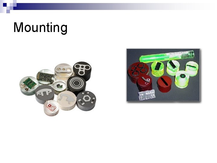
Sample preparation Mounting Grinding Etching Polishing

Mounting


Sectioning, Cutting and polishing

Etching

Effect of Etching Unetched Steel 200 X Etched Steel 200 X Unetched Brass 200 X Etched Brass 200 X

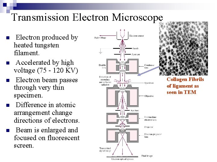
Transmission Electron Microscope n n n Electron produced by heated tungsten filament. Accelerated by high voltage (75 - 120 KV) Electron beam passes through very thin specimen. Difference in atomic arrangement change directions of electrons. Beam is enlarged and focused on fluorescent screen. Collagen Fibrils of ligament as seen in TEM

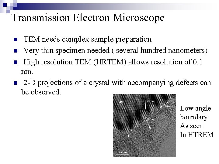
Transmission Electron Microscope n n TEM needs complex sample preparation Very thin specimen needed ( several hundred nanometers) High resolution TEM (HRTEM) allows resolution of 0. 1 nm. 2 -D projections of a crystal with accompanying defects can be observed. Low angle boundary As seen In HTREM

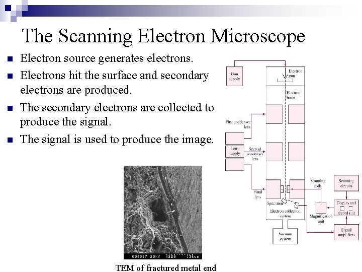
The Scanning Electron Microscope n n Electron source generates electrons. Electrons hit the surface and secondary electrons are produced. The secondary electrons are collected to produce the signal. The signal is used to produce the image. TEM of fractured metal end

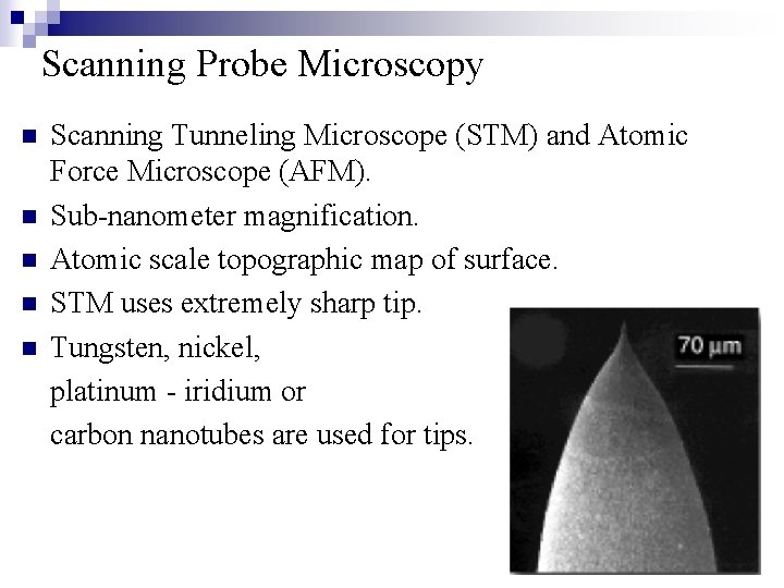
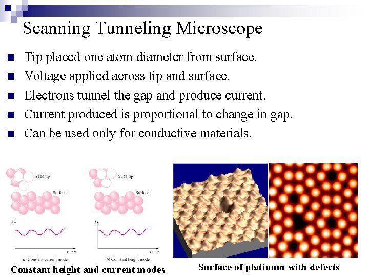
Scanning Probe Microscopy n n n Scanning Tunneling Microscope (STM) and Atomic Force Microscope (AFM). Sub-nanometer magnification. Atomic scale topographic map of surface. STM uses extremely sharp tip. Tungsten, nickel, platinum - iridium or carbon nanotubes are used for tips.

Scanning Tunneling Microscope n n n Tip placed one atom diameter from surface. Voltage applied across tip and surface. Electrons tunnel the gap and produce current. Current produced is proportional to change in gap. Can be used only for conductive materials. Constant height and current modes Surface of platinum with defects

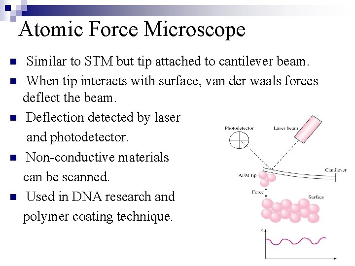
Atomic Force Microscope n n n Similar to STM but tip attached to cantilever beam. When tip interacts with surface, van der waals forces deflect the beam. Deflection detected by laser and photodetector. Non-conductive materials can be scanned. Used in DNA research and polymer coating technique.

ASSIGNMENT #1 n PRIMARY BONDS 1. Ionic bonds Covalent bonds Metallic bonds 2. 3. n SECONDARY BONDS 1. Permanent Dipole bonds Fluctuating Dipole bonds 2. n Point defect – vacancy - interstitially – frenkel - schottky 1. Line defect – dislocations 2. Planar defect – grain boundaries - twin boundaries 3.