CSC 2224 Parallel Computer Architecture and Programming Advanced








- Slides: 95

CSC 2224: Parallel Computer Architecture and Programming Advanced Memory Prof. Gennady Pekhimenko University of Toronto Fall 2019 The content of this lecture is adapted from the slides of Vivek Seshadri, Yoongu Kim, and lectures of Onur Mutlu @ ETH and CMU

Review #5 Flipping Bits in Memory Without Accessing Them Yoongu Kim et al. , ISCA 2014 2

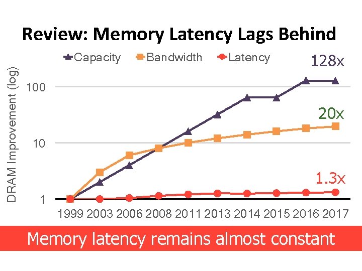
Review: Memory Latency Lags Behind DRAM Improvement (log) Capacity Bandwidth Latency 128 x 100 20 x 10 1. 3 x 1 1999 2003 2006 2008 2011 2013 2014 2015 2016 2017 Memory latency remains almost constant

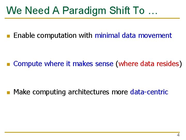
We Need A Paradigm Shift To … Enable computation with minimal data movement Compute where it makes sense (where data resides) Make computing architectures more data-centric 4

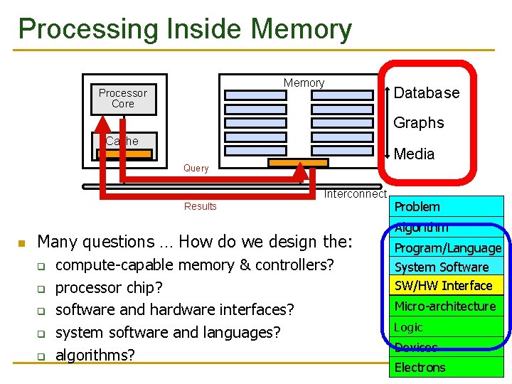
Processing Inside Memory Processor Core Database Graphs Cache Media Query Interconnect Results Many questions … How do we design the: q q q compute-capable memory & controllers? processor chip? software and hardware interfaces? system software and languages? algorithms? Problem Algorithm Program/Language System Software SW/HW Interface Micro-architecture Logic Devices Electrons

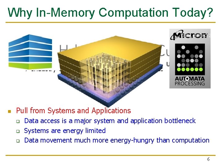
Why In-Memory Computation Today? Push from Technology q Dally, Hi. PEAC 2015 DRAM Scaling at jeopardy Controllers close to DRAM Industry open to new memory architectures Pull from Systems and Applications q q q Data access is a major system and application bottleneck Systems are energy limited Data movement much more energy-hungry than computation 6

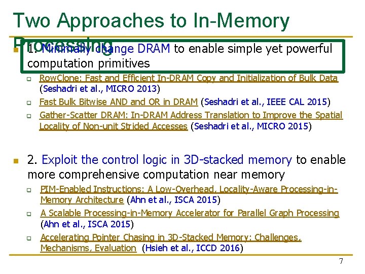
Two Approaches to In-Memory Processing 1. Minimally change DRAM to enable simple yet powerful computation primitives q q q Row. Clone: Fast and Efficient In-DRAM Copy and Initialization of Bulk Data (Seshadri et al. , MICRO 2013) Fast Bulk Bitwise AND and OR in DRAM (Seshadri et al. , IEEE CAL 2015) Gather-Scatter DRAM: In-DRAM Address Translation to Improve the Spatial Locality of Non-unit Strided Accesses (Seshadri et al. , MICRO 2015) 2. Exploit the control logic in 3 D-stacked memory to enable more comprehensive computation near memory q q q PIM-Enabled Instructions: A Low-Overhead, Locality-Aware Processing-in. Memory Architecture (Ahn et al. , ISCA 2015) A Scalable Processing-in-Memory Accelerator for Parallel Graph Processing (Ahn et al. , ISCA 2015) Accelerating Pointer Chasing in 3 D-Stacked Memory: Challenges, Mechanisms, Evaluation (Hsieh et al. , ICCD 2016) 7

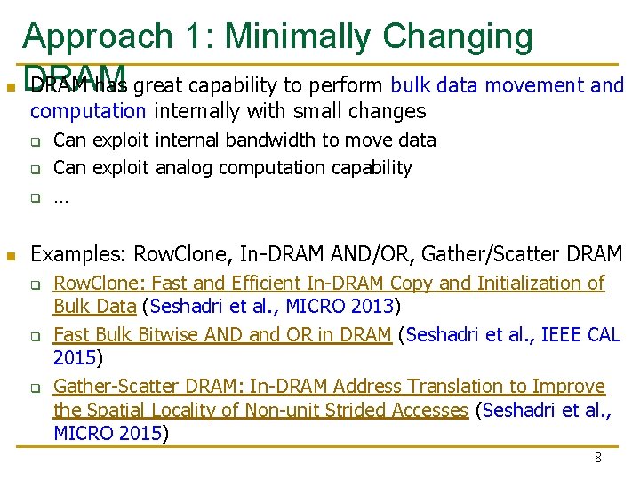
Approach 1: Minimally Changing DRAM has great capability to perform bulk data movement and computation internally with small changes q q q Can exploit internal bandwidth to move data Can exploit analog computation capability … Examples: Row. Clone, In-DRAM AND/OR, Gather/Scatter DRAM q q q Row. Clone: Fast and Efficient In-DRAM Copy and Initialization of Bulk Data (Seshadri et al. , MICRO 2013) Fast Bulk Bitwise AND and OR in DRAM (Seshadri et al. , IEEE CAL 2015) Gather-Scatter DRAM: In-DRAM Address Translation to Improve the Spatial Locality of Non-unit Strided Accesses (Seshadri et al. , MICRO 2015) 8

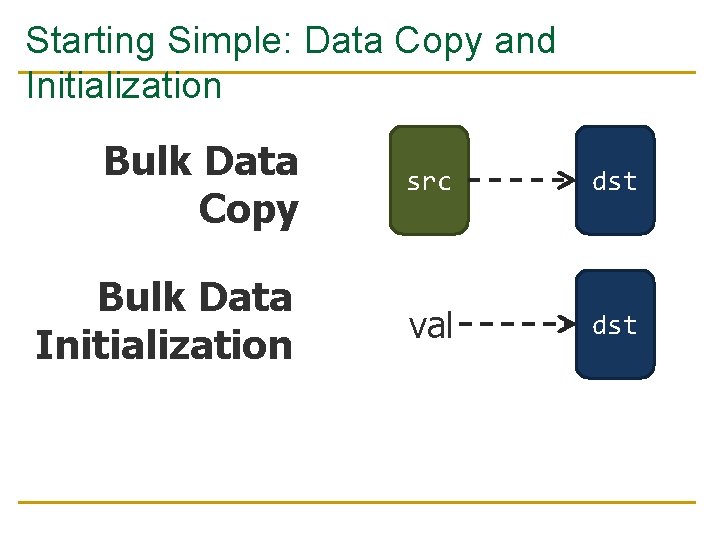
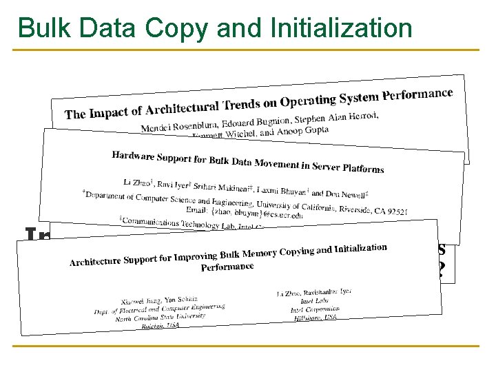
Starting Simple: Data Copy and Initialization Bulk Data Copy src dst Bulk Data Initialization val dst

Bulk Data Copy and Initialization Bulk Data Copy src dst Bulk Data Initialization val dst

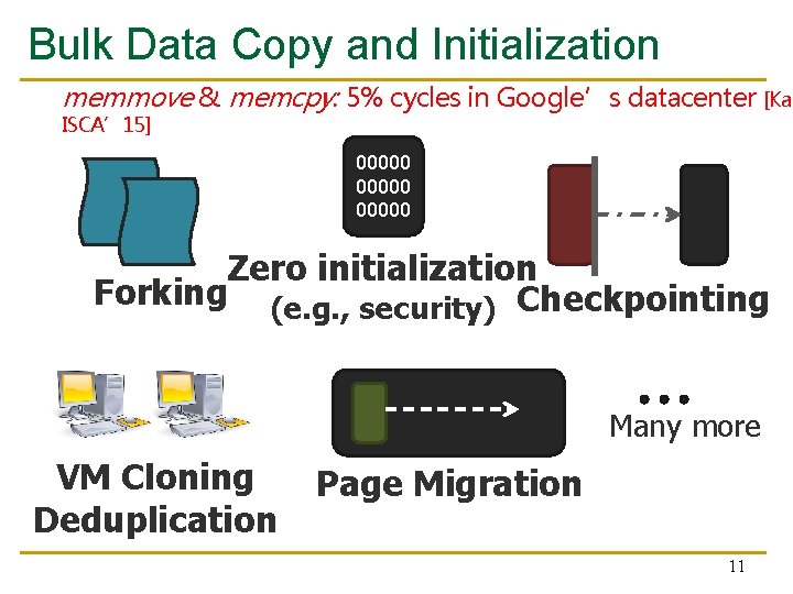
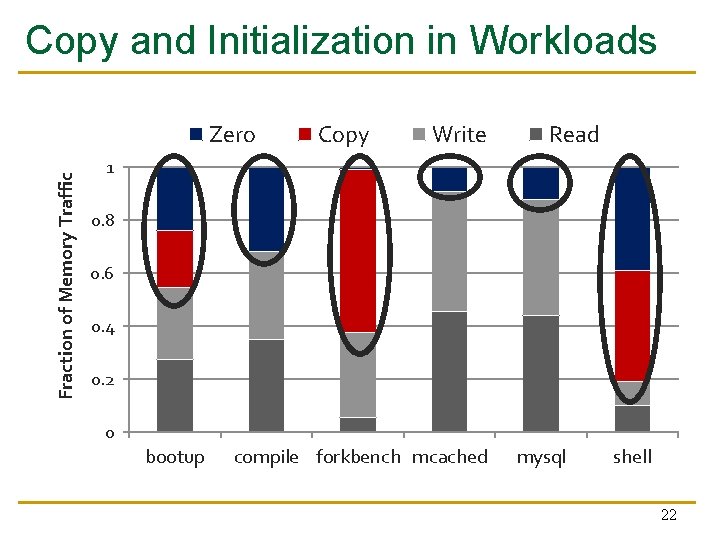
Bulk Data Copy and Initialization memmove & memcpy: 5% cycles in Google’s datacenter [Kan ISCA’ 15] 00000 Zero initialization Forking (e. g. , security) Checkpointing Many more VM Cloning Deduplication Page Migration 11

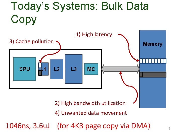
Today’s Systems: Bulk Data Copy 1) High latency 3) Cache pollution CPU L 1 Memory L 2 L 3 MC 2) High bandwidth utilization 4) Unwanted data movement 1046 ns, 3. 6 u. J (for 4 KB page copy via DMA) 12

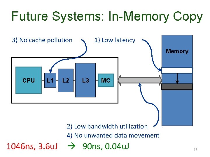
Future Systems: In-Memory Copy 3) No cache pollution 1) Low latency Memory CPU L 1 L 2 L 3 MC 2) Low bandwidth utilization 4) No unwanted data movement 1046 ns, 3. 6 u. J 90 ns, 0. 04 u. J 13

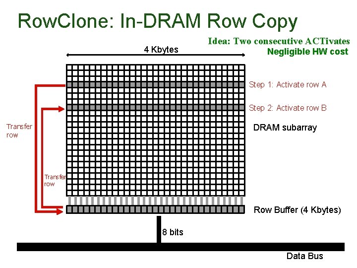
Row. Clone: In-DRAM Row Copy 4 Kbytes Idea: Two consecutive ACTivates Negligible HW cost Step 1: Activate row A Step 2: Activate row B Transfer row DRAM subarray Transfer row Row Buffer (4 Kbytes) 8 bits Data Bus

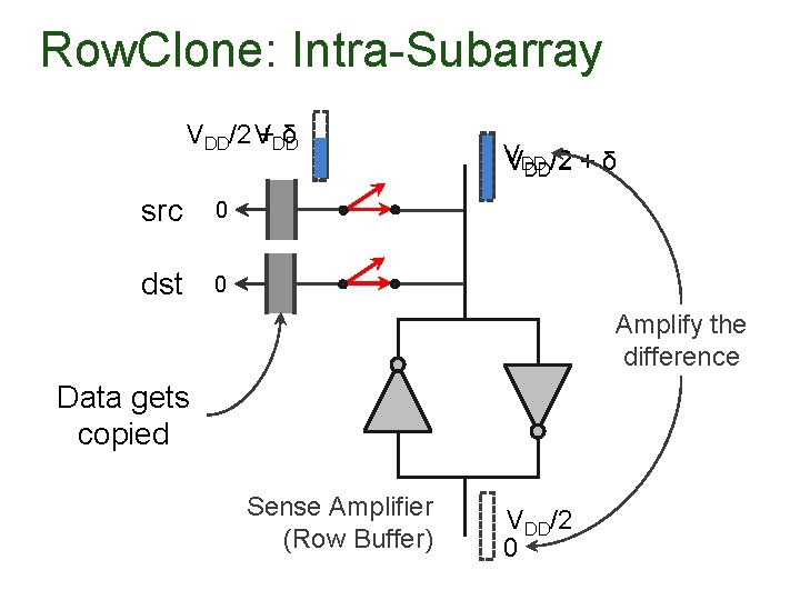
Row. Clone: Intra-Subarray VDD/2 V +DD δ src 0 dst 0 V VDD DD/2 + δ Amplify the difference Data gets copied Sense Amplifier (Row Buffer) VDD/2 0

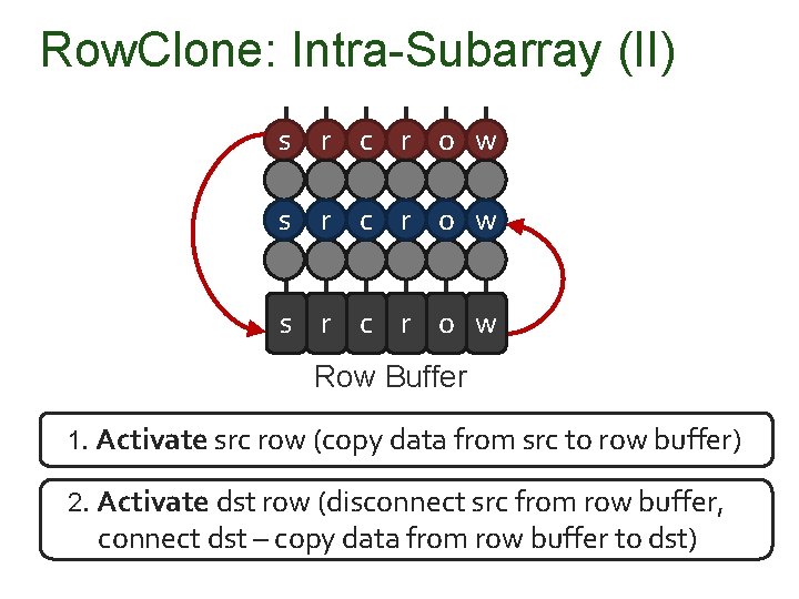
Row. Clone: Intra-Subarray (II) s r c r o w ds sr ct r o w s r c r o w Row Buffer 1. Activate src row (copy data from src to row buffer) 2. Activate dst row (disconnect src from row buffer, connect dst – copy data from row buffer to dst)

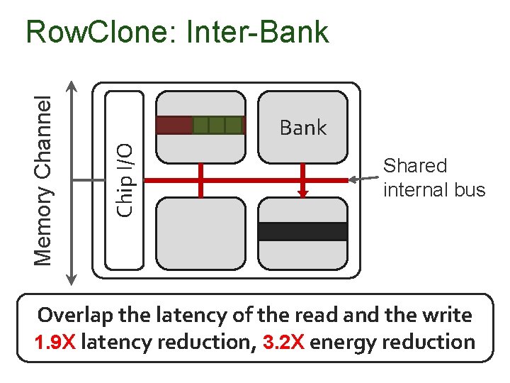
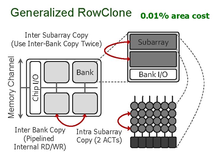
Bank Chip I/O Memory Channel Row. Clone: Inter-Bank Shared internal bus Overlap the latency of the read and the write 1. 9 X latency reduction, 3. 2 X energy reduction

Generalized Row. Clone Chip I/O Memory Channel Inter Subarray Copy (Use Inter-Bank Copy Twice) Inter Bank Copy (Pipelined Internal RD/WR) Bank Intra Subarray Copy (2 ACTs) 0. 01% area cost Subarray Bank I/O

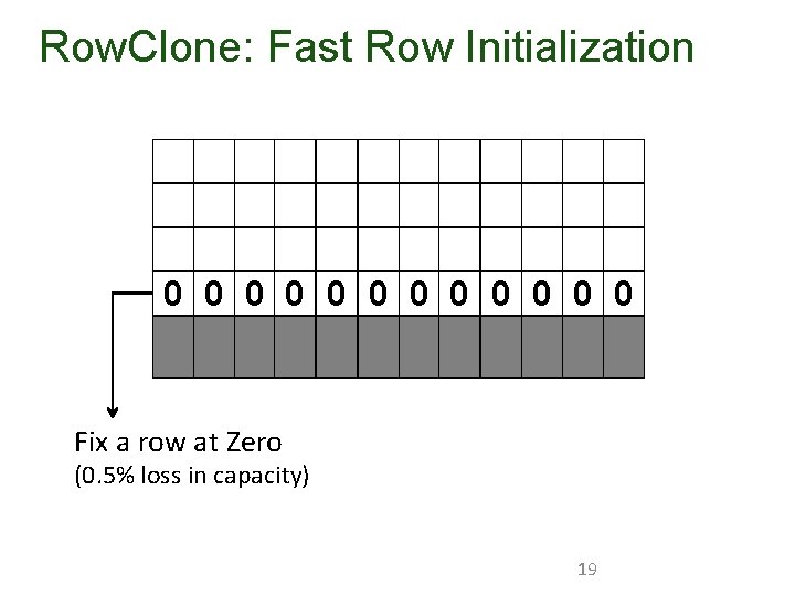
Row. Clone: Fast Row Initialization 0 0 0 Fix a row at Zero (0. 5% loss in capacity) 19

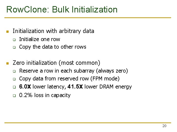
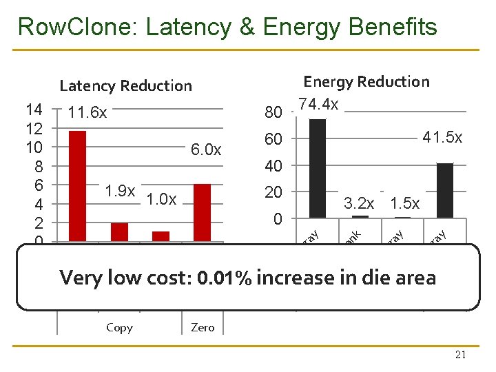
Row. Clone: Bulk Initialization with arbitrary data q q Initialize one row Copy the data to other rows Zero initialization (most common) q q Reserve a row in each subarray (always zero) Copy data from reserved row (FPM mode) 6. 0 X lower latency, 41. 5 X lower DRAM energy 0. 2% loss in capacity 20

Row. Clone: Latency & Energy Benefits Energy Reduction 74. 4 x Latency Reduction 40 20 3. 2 x 1. 5 x y ar ra ub an -B In te r ub tra -S ar ra y y ar ra an ar ra y k 0 y 1. 9 x 1. 0 x 41. 5 x 60 tra -S 6. 0 x Copy In In te r tra -S In ub ub -S te r In In te r -B Very low cost: 0. 01% increase in die area ub tra -S In 80 ub ar ra 11. 6 x -S 14 12 10 8 6 4 2 0 Zero 21

Copy and Initialization in Workloads Fraction of Memory Traffic Zero Copy Write Read 1 0. 8 0. 6 0. 4 0. 2 0 bootup compile forkbench mcached mysql shell 22

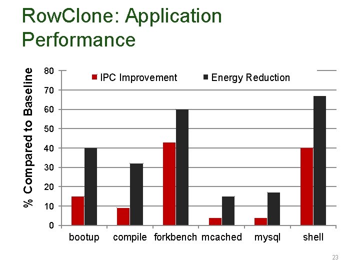
% Compared to Baseline Row. Clone: Application Performance 80 IPC Improvement Energy Reduction 70 60 50 40 30 20 10 0 bootup compile forkbench mcached mysql shell 23

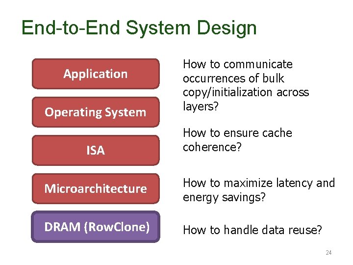
End-to-End System Design Application Operating System ISA How to communicate occurrences of bulk copy/initialization across layers? How to ensure cache coherence? Microarchitecture How to maximize latency and energy savings? DRAM (Row. Clone) How to handle data reuse? 24

Ambit In-Memory Accelerator for Bulk Bitwise Operations Using Commodity DRAM Technology Vivek Seshadri Donghyuk Lee, Thomas Mullins, Hasan Hassan, Amirali Boroumand, Jeremie Kim, Michael A. Kozuch, Onur Mutlu, Phillip B. Gibbons, Todd C. Mowry

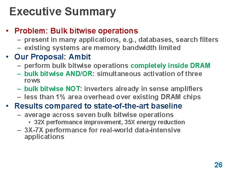
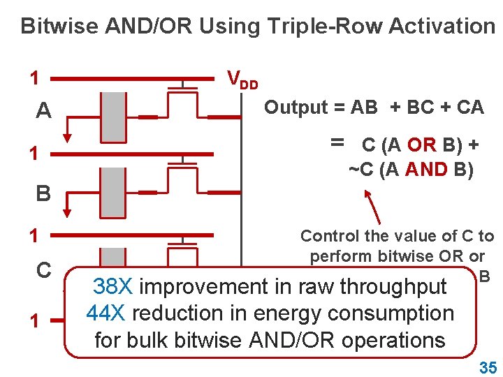
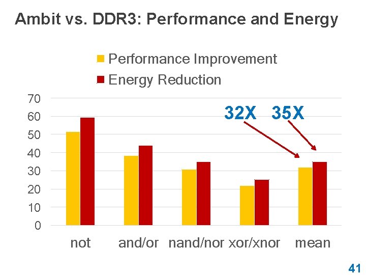
Executive Summary • Problem: Bulk bitwise operations – present in many applications, e. g. , databases, search filters – existing systems are memory bandwidth limited • Our Proposal: Ambit – perform bulk bitwise operations completely inside DRAM – bulk bitwise AND/OR: simultaneous activation of three rows – bulk bitwise NOT: inverters already in sense amplifiers – less than 1% area overhead over existing DRAM chips • Results compared to state-of-the-art baseline – average across seven bulk bitwise operations • 32 X performance improvement, 35 X energy reduction – 3 X-7 X performance for real-world data-intensive applications 26

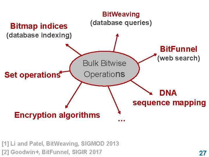
Bitmap indices Bit. Weaving (database queries) (database indexing) Bit. Funnel Set operations Bulk Bitwise Operations (web search) DNA sequence mapping Encryption algorithms . . . [1] Li and Patel, Bit. Weaving, SIGMOD 2013 [2] Goodwin+, Bit. Funnel, SIGIR 2017 27

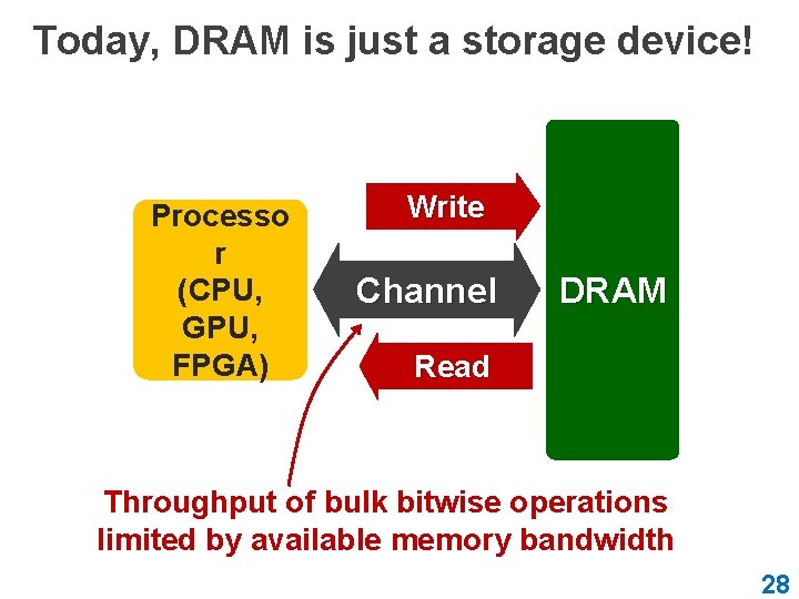
Today, DRAM is just a storage device! Processo r (CPU, GPU, FPGA) Write Channel DRAM Read Throughput of bulk bitwise operations limited by available memory bandwidth 28

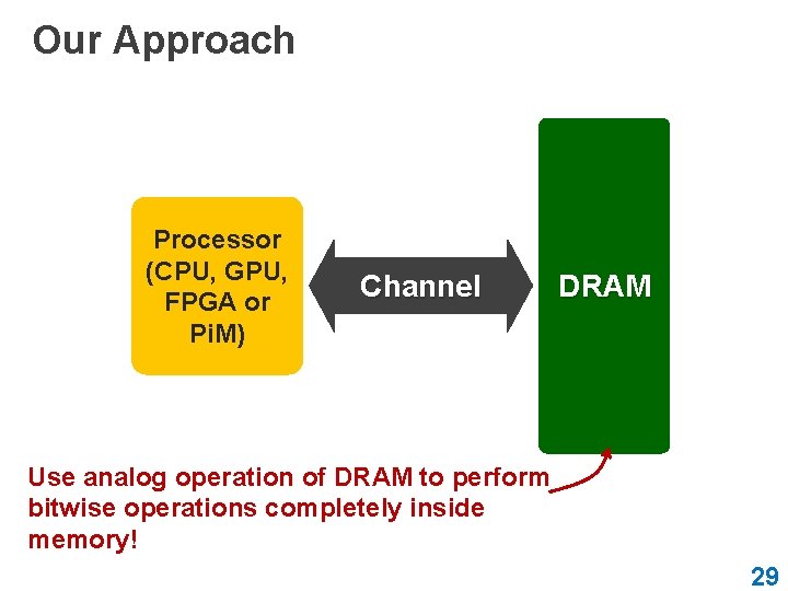
Our Approach Processor (CPU, GPU, FPGA or Pi. M) Channel DRAM Use analog operation of DRAM to perform bitwise operations completely inside memory! 29

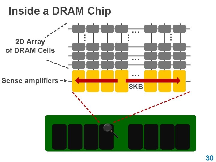
Inside a DRAM Chip … … Sense amplifiers … 2 D Array of DRAM Cells … … … 8 KB 30

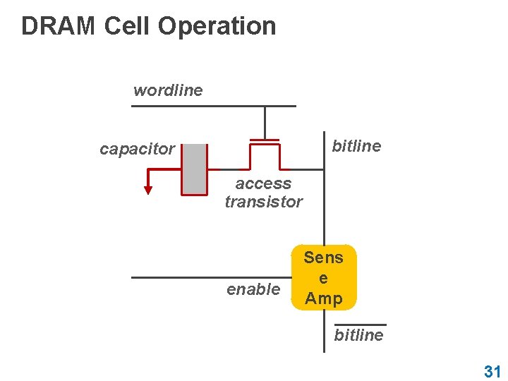
DRAM Cell Operation wordline bitline capacitor access transistor enable Sens e Amp bitline 31

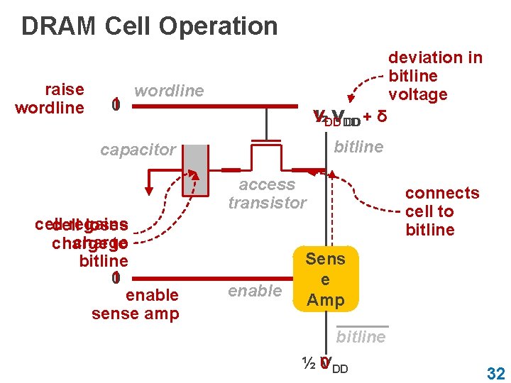
DRAM Cell Operation raise wordline 1 0 deviation in bitline voltage wordline ½ VDD DD + δ bitline capacitor access transistor cell regains cell loses charge to bitline 1 0 enable sense amp enable connects cell to bitline Sens e Amp bitline ½ 0 VDD 32

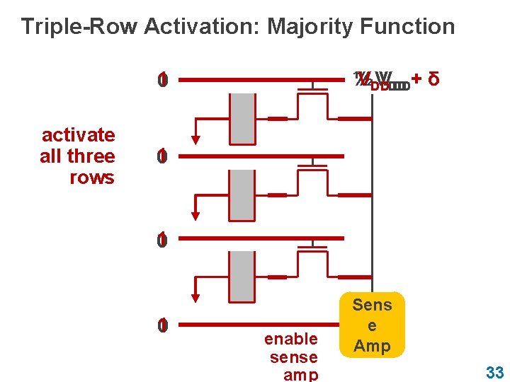
Triple-Row Activation: Majority Function 1 0 activate all three rows ½ ½ VDD VVDD DD+ δ 1 0 1 0 enable sense amp Sens e Amp 33

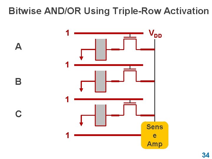
Bitwise AND/OR Using Triple-Row Activation 1 VDD A 1 B 1 C 1 Sens e Amp 34

Bitwise AND/OR Using Triple-Row Activation 1 A 1 VDD Output = AB + BC + CA = C (A OR B) + ~C (A AND B) B 1 Control the value of C to perform bitwise OR or bitwise AND of A and B 38 X improvement in raw throughput Sens 44 X reduction ine energy consumption Amp for bulk bitwise AND/OR operations 35

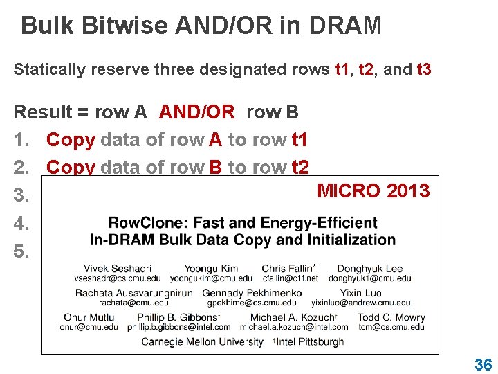
Bulk Bitwise AND/OR in DRAM Statically reserve three designated rows t 1, t 2, and t 3 Result = row A AND/OR row B 1. Copy data of row A to row t 1 2. Copy data of row B to row t 2 3. Initialize data of row t 3 to 0/1 MICRO 2013 4. Activate rows t 1/t 2/t 3 simultaneously 5. Copy data of row t 1/t 2/t 3 to Result row 36

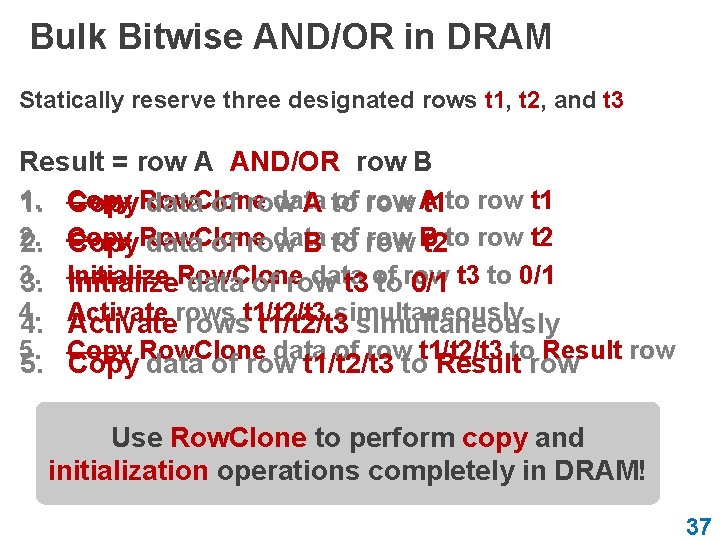
Bulk Bitwise AND/OR in DRAM Statically reserve three designated rows t 1, t 2, and t 3 Result = row A AND/OR row B 1. Copy data of row A Copy. Row. Clone data of row A to t 1 to row t 1 2. data of row B 2. Copy. Row. Clone data of row B to t 2 to row t 2 3. data 3. Initialize. Row. Clone data of row t 3 of torow 0/1 t 3 to 0/1 4. simultaneously 4. Activaterowst 1/t 2/t 3 simultaneously 5. Copy Row. Clone data of row t 1/t 2/t 3 to Result row 5. Copy data of row t 1/t 2/t 3 to Result row Use Row. Clone to perform copy and initialization operations completely in DRAM! 37

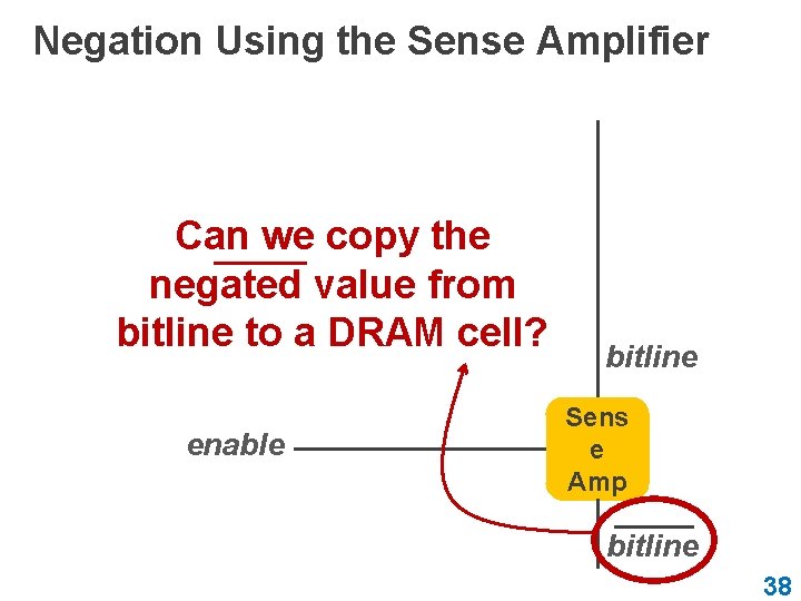
Negation Using the Sense Amplifier Can we copy the negated value from bitline to a DRAM cell? enable bitline Sens e Amp bitline 38

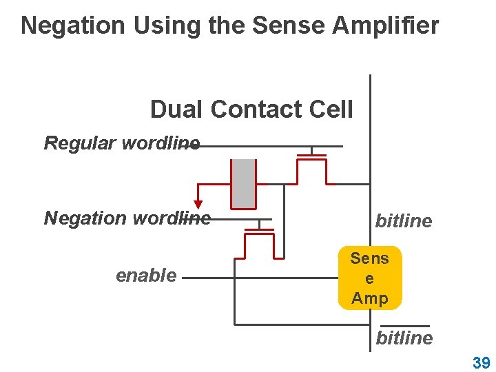
Negation Using the Sense Amplifier Dual Contact Cell Regular wordline Negation wordline enable bitline Sens e Amp bitline 39

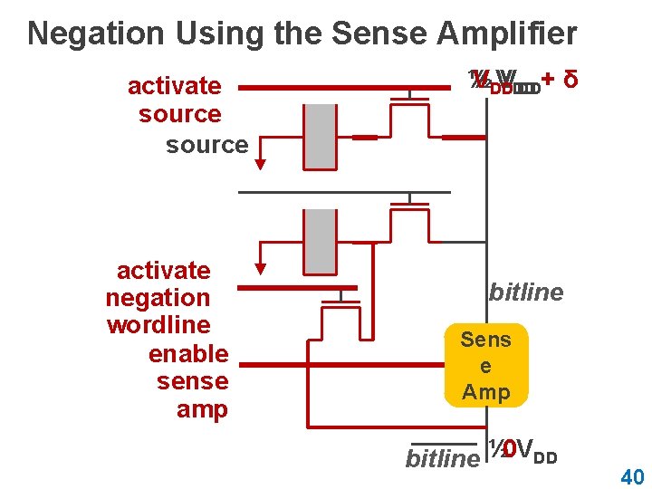
Negation Using the Sense Amplifier activate source activate negation wordline enable sense amp ½ ½ VDD VVDD DD+ δ bitline Sens e Amp bitline ½ 0 VDD 40

Ambit vs. DDR 3: Performance and Energy Performance Improvement Energy Reduction 70 60 50 40 30 20 10 0 32 X 35 X not and/or nand/nor xor/xnor mean 41

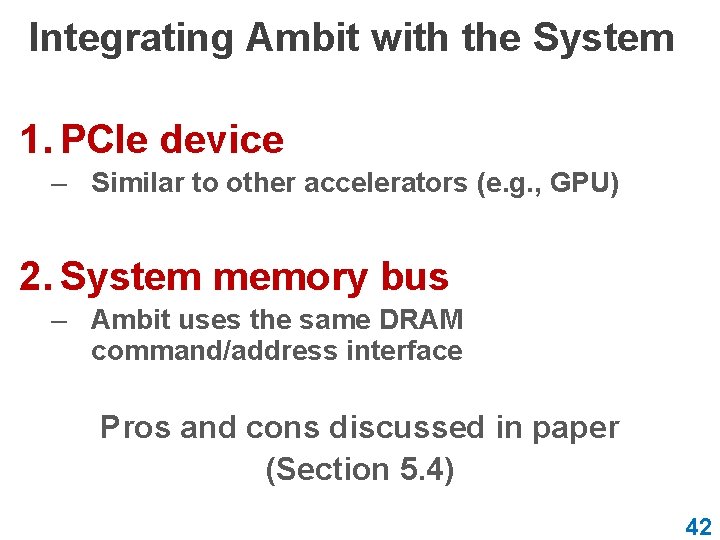
Integrating Ambit with the System 1. PCIe device – Similar to other accelerators (e. g. , GPU) 2. System memory bus – Ambit uses the same DRAM command/address interface Pros and cons discussed in paper (Section 5. 4) 42

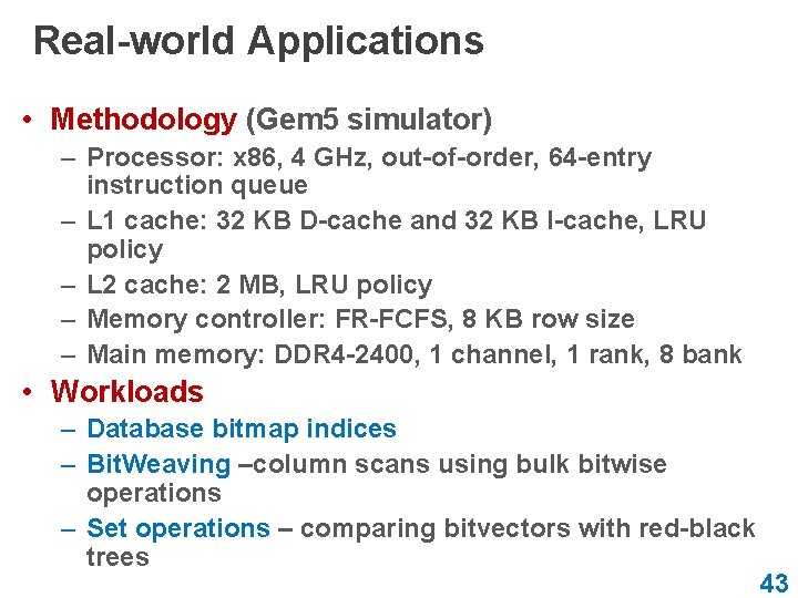
Real-world Applications • Methodology (Gem 5 simulator) – Processor: x 86, 4 GHz, out-of-order, 64 -entry instruction queue – L 1 cache: 32 KB D-cache and 32 KB I-cache, LRU policy – L 2 cache: 2 MB, LRU policy – Memory controller: FR-FCFS, 8 KB row size – Main memory: DDR 4 -2400, 1 channel, 1 rank, 8 bank • Workloads – Database bitmap indices – Bit. Weaving –column scans using bulk bitwise operations – Set operations – comparing bitvectors with red-black trees 43

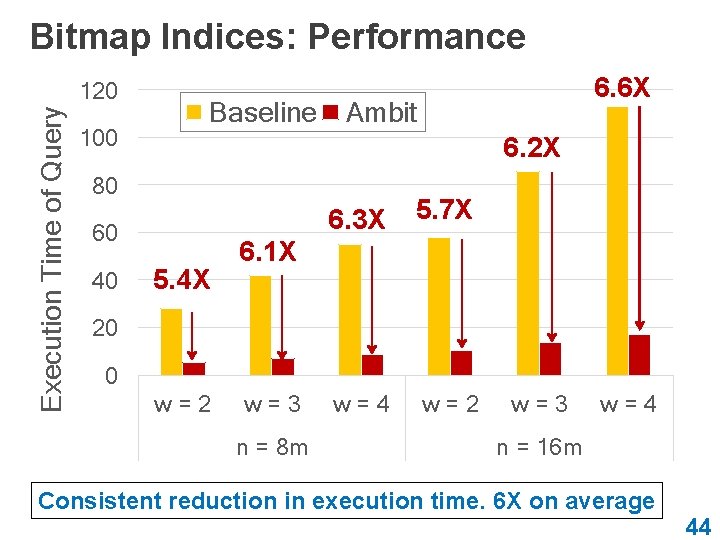
Bitmap Indices: Performance Execution Time of Query 120 100 Baseline Ambit 6. 2 X 80 60 40 6. 6 X 5. 4 X 6. 3 X 5. 7 X w=4 w=2 6. 1 X 20 0 w=2 w=3 n = 8 m w=3 w=4 n = 16 m Consistent reduction in execution time. 6 X on average 44

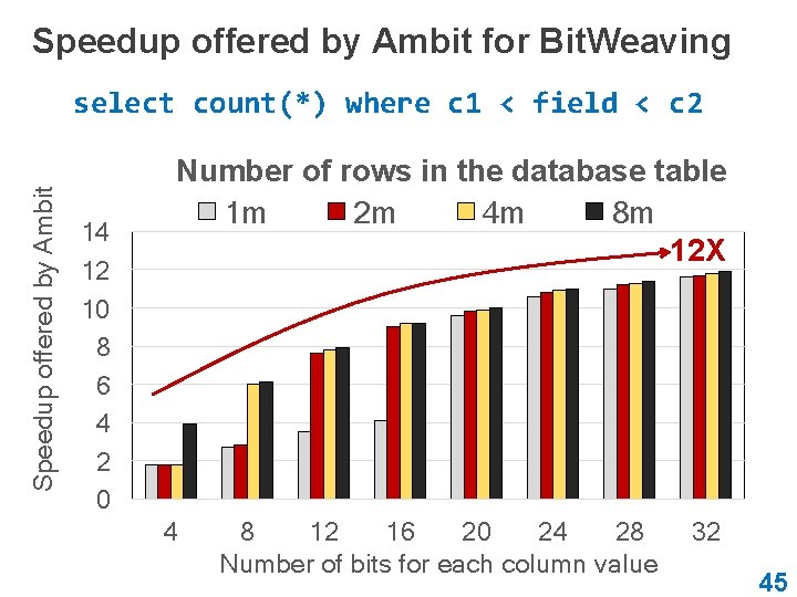
Speedup offered by Ambit for Bit. Weaving Speedup offered by Ambit select count(*) where c 1 < field < c 2 14 12 10 8 6 4 2 0 Number of rows in the database table 1 m 2 m 4 m 8 m 12 X 4 8 12 16 20 24 28 Number of bits for each column value 32 45

FLIPPING BITS IN MEMORY WITHOUT ACCESSING THEM ISCA 2014 ROW HAMMER 46

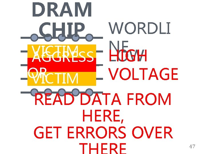
DRAM CHIP WORDLI NE VICTIM LOW AGGRESS HIGH ROW OR VOLTAGE VICTIM READ DATA FROM HERE, GET ERRORS OVER 47

GOOGLE’S EXPLOIT “We learned about rowhammer from Yoongu Kim et al. ” http: //googleprojectzero. blogspot. com 48

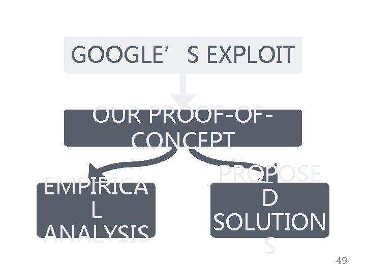
GOOGLE’S EXPLOIT OUR PROOF-OFCONCEPT PROPOSE EMPIRICA D L SOLUTION ANALYSIS S 49

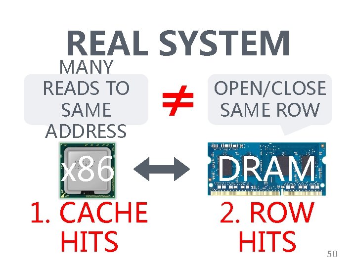
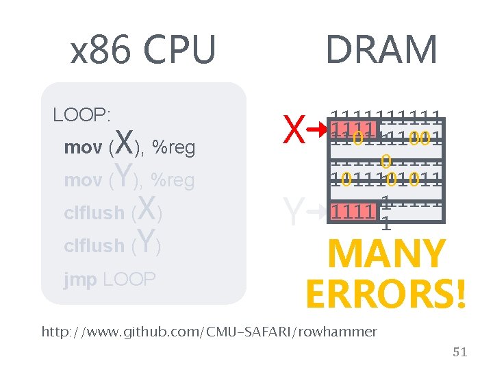
REAL SYSTEM MANY READS TO SAME ADDRESS ≠ OPEN/CLOSE SAME ROW x 86 DRAM 1. CACHE HITS 2. ROW HITS 50

x 86 CPU DRAM mov (X), %reg X clflush (X) Y LOOP: mov (Y), %reg clflush (Y) jmp LOOP 1111111111 1101111001 1 11111 1 0 11111 1011101011 1 11111 1 1 MANY ERRORS! http: //www. github. com/CMU-SAFARI/rowhammer 51

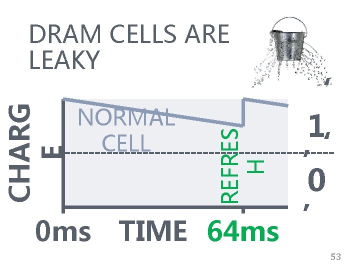
WHY DO THE ERRORS OCCUR? 52

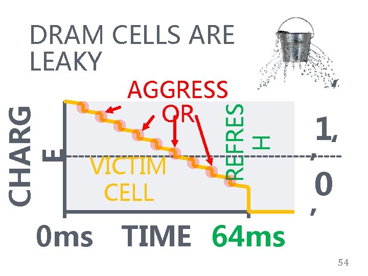
DRAM CELLS ARE LEAKY REFRES H CHARG E ‘ NORMAL 1 CELL ‘ ’ 0 ms TIME 64 ms 53

DRAM CELLS ARE LEAKY REFRES H CHARG E ‘ 1 ‘ VICTIM ’ 0 CELL ’ 0 ms TIME 64 ms AGGRESS OR 54

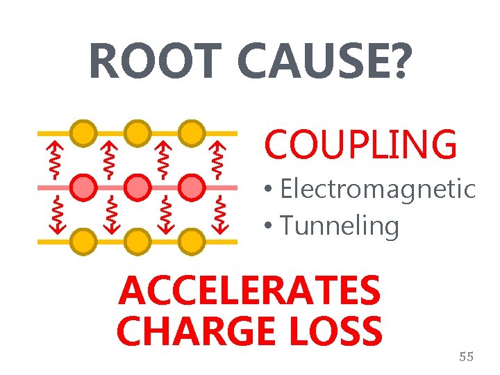
⇝ ⇝ ROOT CAUSE? COUPLING ⇝ ⇝ • Electromagnetic • Tunneling ACCELERATES CHARGE LOSS 55

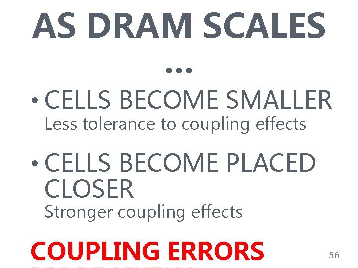
AS DRAM SCALES … • CELLS BECOME SMALLER Less tolerance to coupling effects • CELLS BECOME PLACED CLOSER Stronger coupling effects COUPLING ERRORS 56

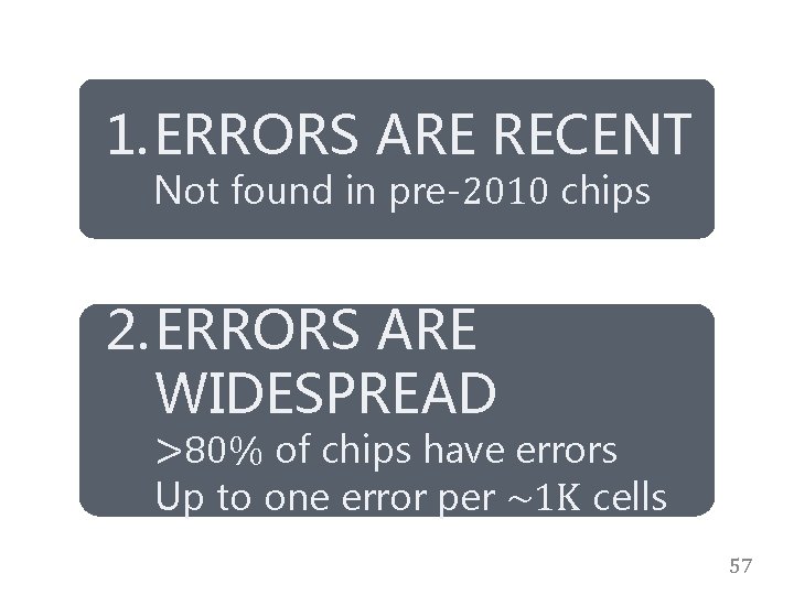
1. ERRORS ARE RECENT Not found in pre-2010 chips 2. ERRORS ARE WIDESPREAD >80% of chips have errors Up to one error per ~1 K cells 57

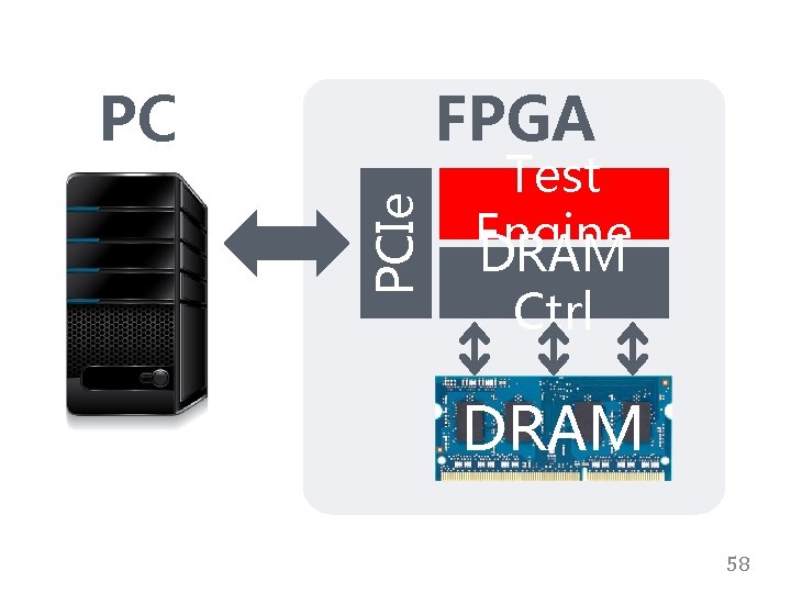
FPGA PCIe PC Test Engine DRAM Ctrl DRAM 58

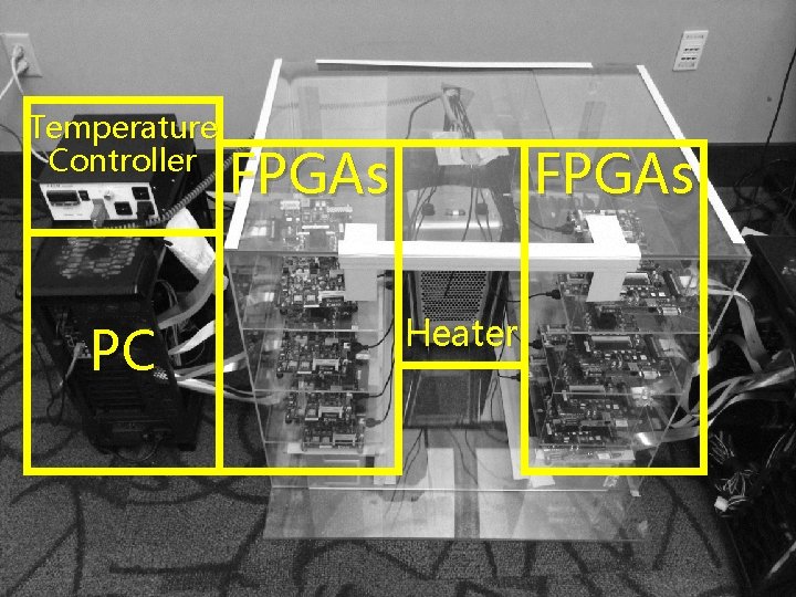
Temperature Controller PC FPGAs Heater

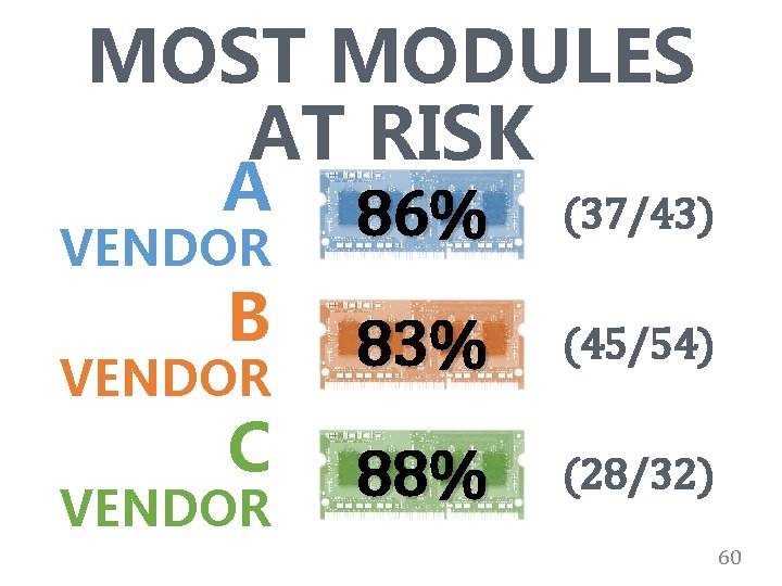
MOST MODULES AT RISK A 86% (37/43) B 83% (45/54) C 88% (28/32) VENDOR 60

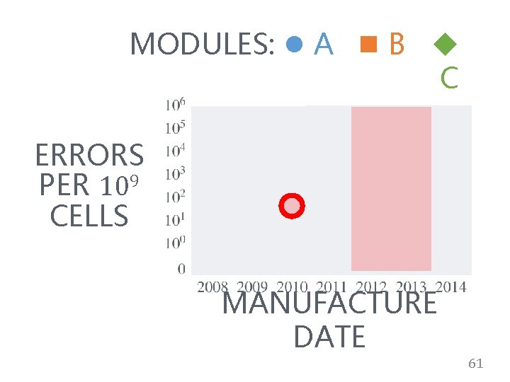
MODULES: A B C ERRORS PER 109 CELLS MANUFACTURE DATE 61

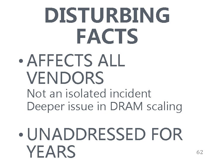
DISTURBING FACTS • AFFECTS ALL VENDORS Not an isolated incident Deeper issue in DRAM scaling • UNADDRESSED FOR YEARS 62

HOW TO PREVENT COUPLING Previous Approaches ERRORS? 1. Make Better Chips: Expensive 2. Rigorous Testing: Takes Too Long 63

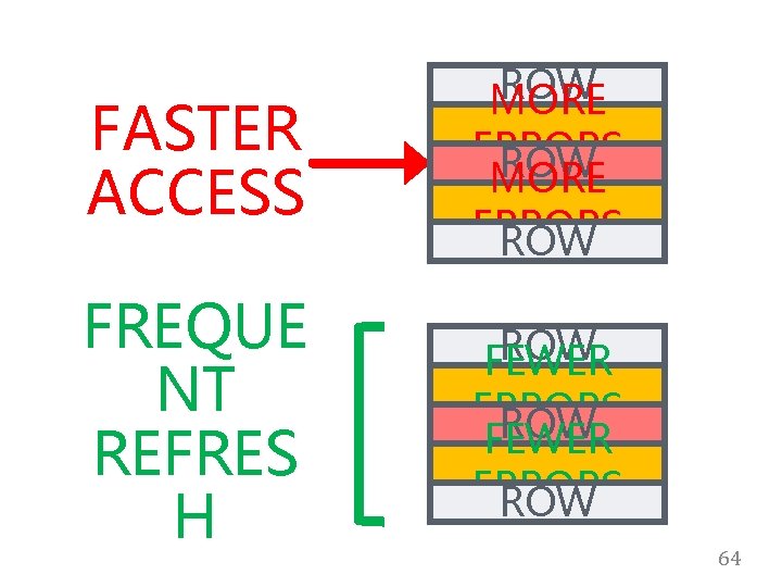
FASTER ACCESS ROW MORE ERRORS ROW FREQUE NT REFRES H ROW FEWER ERRORS ROW 64

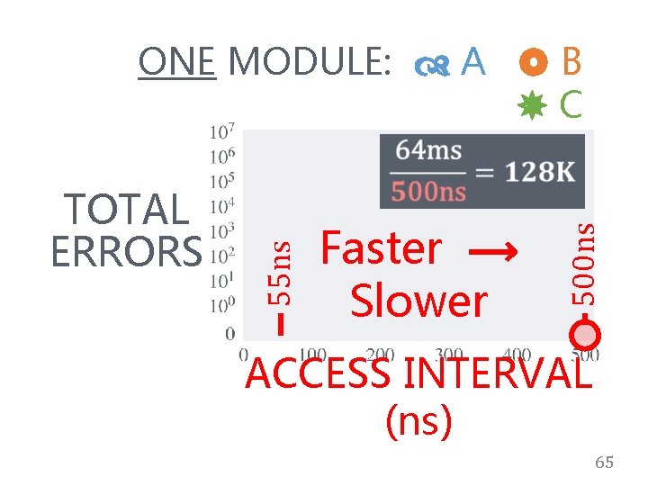
Faster ⟶ Slower 500 ns TOTAL ERRORS 55 ns ONE MODULE: A B C ACCESS INTERVAL (ns) 65

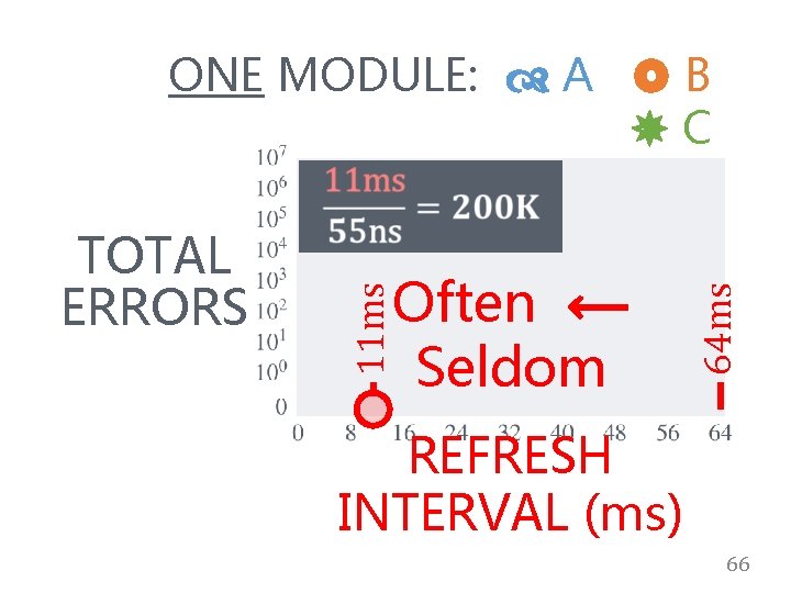
Often ⟵ Seldom 64 ms TOTAL ERRORS 11 ms ONE MODULE: A B C REFRESH INTERVAL (ms) 66

TWO NAIVE SOLUTIONS 1. LIMIT ACCESSES TO ROW Access Interval > 500 ns 2. REFRESH ALL ROWS LARGE OFTEN OVERHEAD: Refresh Interval < 11 ms PERF, ENERGY, COMPLEXITY 67

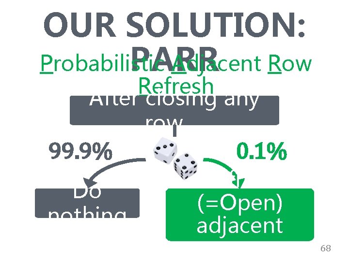
OUR SOLUTION: Probabilistic Adjacent Row PARR Refresh After closing any row. . . 99. 9% Do nothing 0. 1% Refresh (=Open) adjacent rows 68

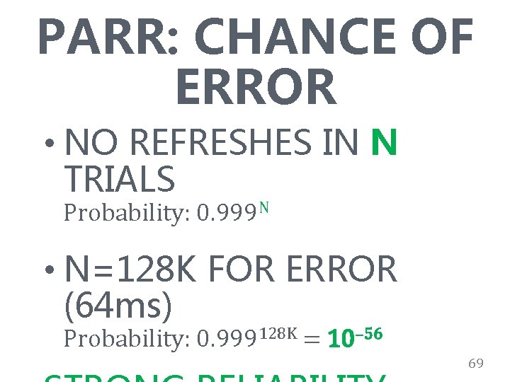
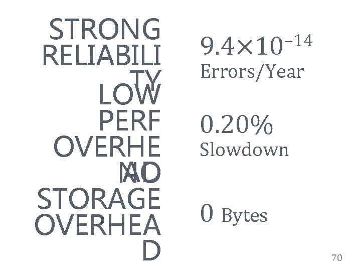
PARR: CHANCE OF ERROR • NO REFRESHES IN N TRIALS Probability: 0. 999 N • N=128 K FOR ERROR (64 ms) Probability: 0. 999128 K = 10– 56 69

STRONG RELIABILI TY LOW PERF OVERHE AD NO STORAGE OVERHEA D – 14 9. 4× 10 Errors/Year 0. 20% Slowdown 0 Bytes 70

RELATED WORK • Security Exploit (Seaborn@Google 2015) • Industry Analysis Hynix 2014) (Kang@SK “. . . will be [more] severe as technology shrinks down. ” • Targeted Row Refresh 2014) (JEDEC • DRAM Testing (e. g. , Van de 71

Emerging Memory Technologies 72

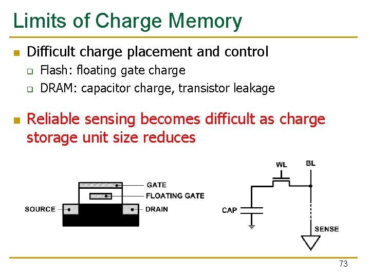
Limits of Charge Memory Difficult charge placement and control q q Flash: floating gate charge DRAM: capacitor charge, transistor leakage Reliable sensing becomes difficult as charge storage unit size reduces 73

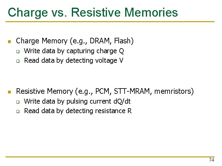
Charge vs. Resistive Memories Charge Memory (e. g. , DRAM, Flash) q q Write data by capturing charge Q Read data by detecting voltage V Resistive Memory (e. g. , PCM, STT-MRAM, memristors) q q Write data by pulsing current d. Q/dt Read data by detecting resistance R 74

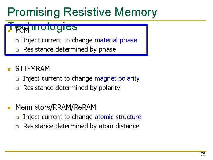
Promising Resistive Memory Technologies PCM q q STT-MRAM q q Inject current to change material phase Resistance determined by phase Inject current to change magnet polarity Resistance determined by polarity Memristors/RRAM/Re. RAM q q Inject current to change atomic structure Resistance determined by atom distance 75

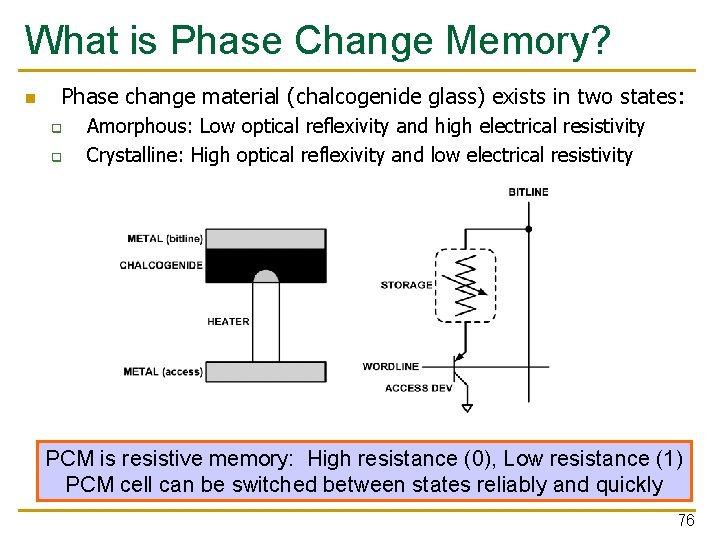
What is Phase Change Memory? Phase change material (chalcogenide glass) exists in two states: q q Amorphous: Low optical reflexivity and high electrical resistivity Crystalline: High optical reflexivity and low electrical resistivity PCM is resistive memory: High resistance (0), Low resistance (1) PCM cell can be switched between states reliably and quickly 76

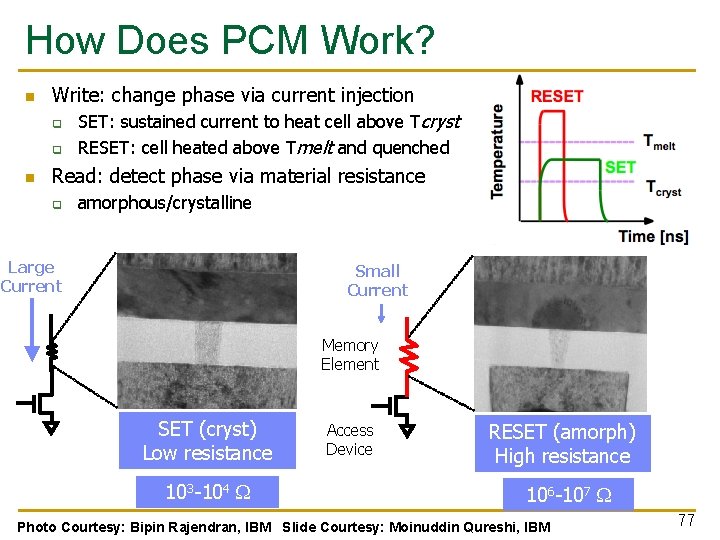
How Does PCM Work? Write: change phase via current injection q q SET: sustained current to heat cell above Tcryst RESET: cell heated above Tmelt and quenched Read: detect phase via material resistance q amorphous/crystalline Large Current Small Current Memory Element SET (cryst) Low resistance 103 -104 W Access Device RESET (amorph) High resistance 106 -107 W Photo Courtesy: Bipin Rajendran, IBM Slide Courtesy: Moinuddin Qureshi, IBM 77

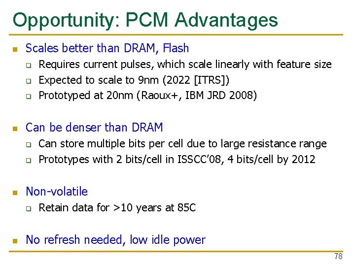
Opportunity: PCM Advantages Scales better than DRAM, Flash q q q Can be denser than DRAM q q Can store multiple bits per cell due to large resistance range Prototypes with 2 bits/cell in ISSCC’ 08, 4 bits/cell by 2012 Non-volatile q Requires current pulses, which scale linearly with feature size Expected to scale to 9 nm (2022 [ITRS]) Prototyped at 20 nm (Raoux+, IBM JRD 2008) Retain data for >10 years at 85 C No refresh needed, low idle power 78

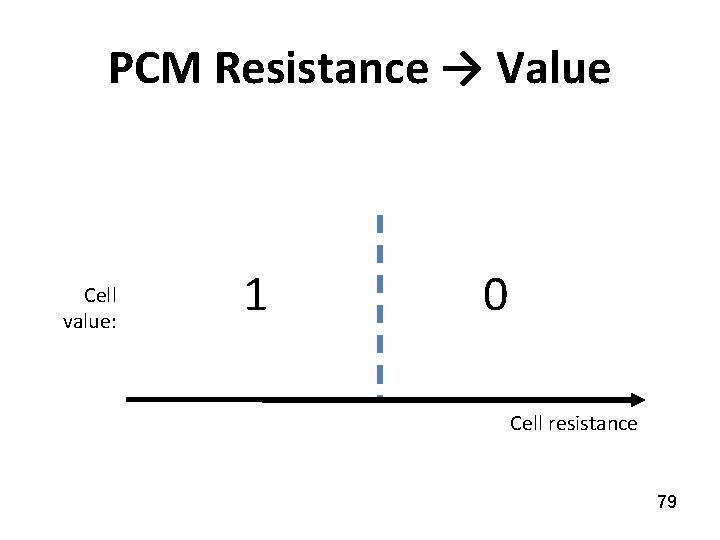
PCM Resistance → Value Cell value: 1 0 Cell resistance 79

Multi-Level Cell PCM Multi-level cell: more than 1 bit per cell Further increases density by 2 to 4 x [Lee+, ISCA'09] But MLC-PCM also has drawbacks Higher latency and energy than single-level cell PCM 80

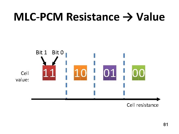
MLC-PCM Resistance → Value Bit 1 Bit 0 Cell value: 11 10 01 00 Cell resistance 81

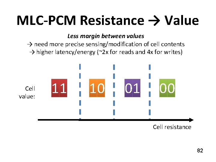
MLC-PCM Resistance → Value Less margin between values → need more precise sensing/modification of cell contents → higher latency/energy (~2 x for reads and 4 x for writes) Cell value: 11 10 01 00 Cell resistance 82

Phase Change Memory Properties Surveyed prototypes from 2003 -2008 (ITRS, IEDM, VLSI, ISSCC) Derived PCM parameters for F=90 nm Lee, Ipek, Mutlu, Burger, “Architecting Phase Change Memory as a Scalable DRAM Alternative, ” ISCA 2009. Lee et al. , “Phase Change Technology and the Future of Main Memory, ” IEEE Micro Top Picks 2010. 83

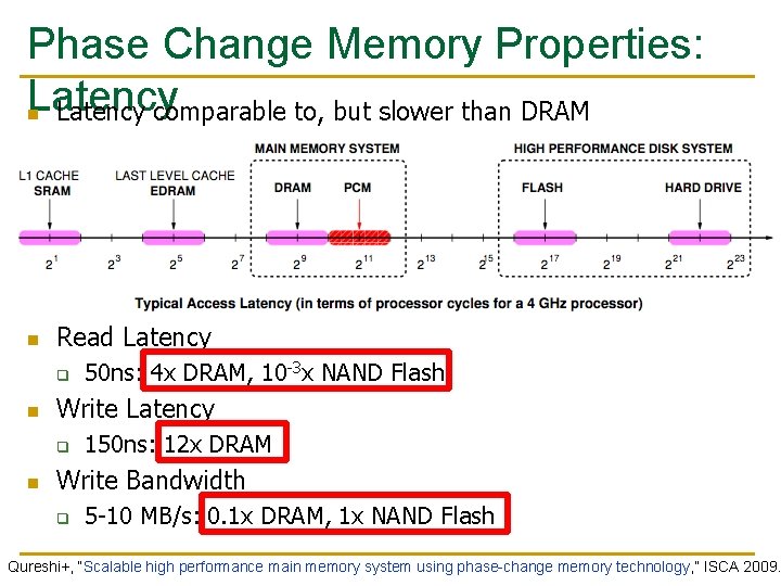
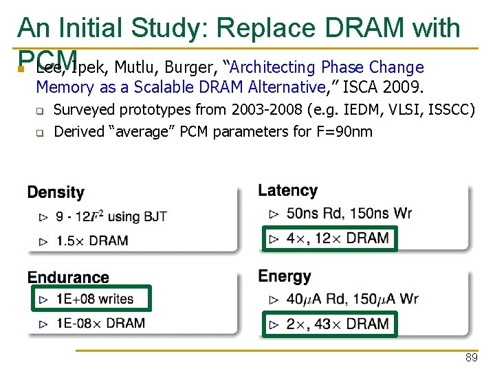
Phase Change Memory Properties: Latency comparable to, but slower than DRAM Read Latency q Write Latency q 50 ns: 4 x DRAM, 10 -3 x NAND Flash 150 ns: 12 x DRAM Write Bandwidth q 5 -10 MB/s: 0. 1 x DRAM, 1 x NAND Flash Qureshi+, “Scalable high performance main memory system using phase-change memory technology, ” ISCA 2009.

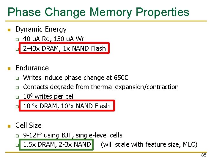
Phase Change Memory Properties Dynamic Energy q q Endurance q q 40 u. A Rd, 150 u. A Wr 2 -43 x DRAM, 1 x NAND Flash Writes induce phase change at 650 C Contacts degrade from thermal expansion/contraction 108 writes per cell 10 -8 x DRAM, 103 x NAND Flash Cell Size q q 9 -12 F 2 using BJT, single-level cells 1. 5 x DRAM, 2 -3 x NAND (will scale with feature size, MLC) 85

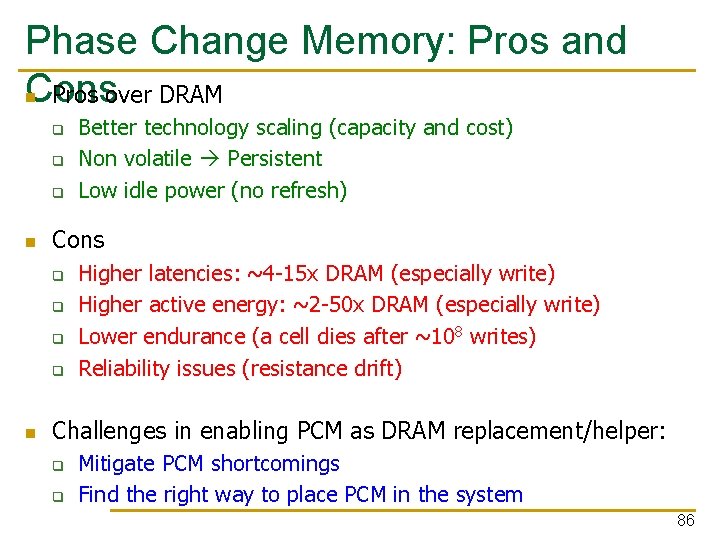
Phase Change Memory: Pros and Cons Pros over DRAM q q q Cons q q Better technology scaling (capacity and cost) Non volatile Persistent Low idle power (no refresh) Higher latencies: ~4 -15 x DRAM (especially write) Higher active energy: ~2 -50 x DRAM (especially write) Lower endurance (a cell dies after ~108 writes) Reliability issues (resistance drift) Challenges in enabling PCM as DRAM replacement/helper: q q Mitigate PCM shortcomings Find the right way to place PCM in the system 86

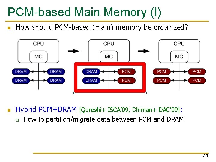
PCM-based Main Memory (I) How should PCM-based (main) memory be organized? Hybrid PCM+DRAM [Qureshi+ ISCA’ 09, Dhiman+ DAC’ 09]: q How to partition/migrate data between PCM and DRAM 87

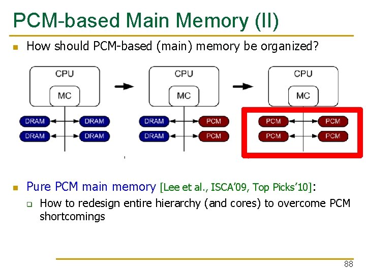
PCM-based Main Memory (II) How should PCM-based (main) memory be organized? Pure PCM main memory [Lee et al. , ISCA’ 09, Top Picks’ 10]: q How to redesign entire hierarchy (and cores) to overcome PCM shortcomings 88

An Initial Study: Replace DRAM with PCM Lee, Ipek, Mutlu, Burger, “Architecting Phase Change Memory as a Scalable DRAM Alternative, ” ISCA 2009. q q Surveyed prototypes from 2003 -2008 (e. g. IEDM, VLSI, ISSCC) Derived “average” PCM parameters for F=90 nm 89

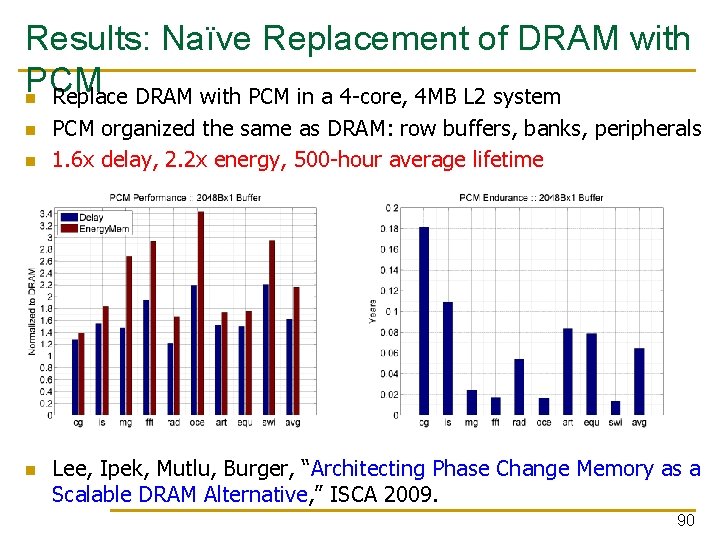
Results: Naïve Replacement of DRAM with PCM Replace DRAM with PCM in a 4 -core, 4 MB L 2 system PCM organized the same as DRAM: row buffers, banks, peripherals 1. 6 x delay, 2. 2 x energy, 500 -hour average lifetime Lee, Ipek, Mutlu, Burger, “Architecting Phase Change Memory as a Scalable DRAM Alternative, ” ISCA 2009. 90

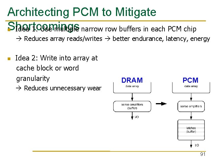
Architecting PCM to Mitigate Shortcomings Idea 1: Use multiple narrow buffers in each PCM chip Reduces array reads/writes better endurance, latency, energy Idea 2: Write into array at cache block or word granularity Reduces unnecessary wear DRAM PCM 91

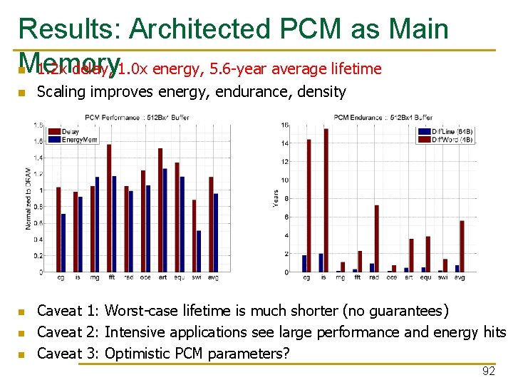
Results: Architected PCM as Main Memory 1. 2 x delay, 1. 0 x energy, 5. 6 -year average lifetime Scaling improves energy, endurance, density Caveat 1: Worst-case lifetime is much shorter (no guarantees) Caveat 2: Intensive applications see large performance and energy hits Caveat 3: Optimistic PCM parameters? 92

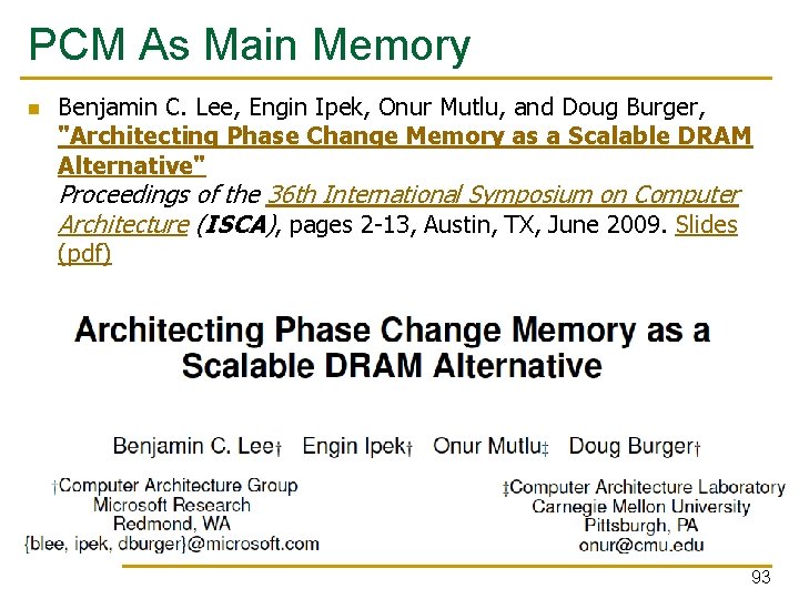
PCM As Main Memory Benjamin C. Lee, Engin Ipek, Onur Mutlu, and Doug Burger, "Architecting Phase Change Memory as a Scalable DRAM Alternative" Proceedings of the 36 th International Symposium on Computer Architecture (ISCA), pages 2 -13, Austin, TX, June 2009. Slides (pdf) 93

Review #5 Flipping Bits in Memory Without Accessing Them Yoongu Kim et al. , ISCA 2014 94

CSC 2224: Parallel Computer Architecture and Programming Advanced Memory Prof. Gennady Pekhimenko University of Toronto Fall 2019 The content of this lecture is adapted from the slides of Vivek Seshadri, Yoongu Kim, and lectures of Onur Mutlu @ ETH and CMU