CSC 2231 Parallel Computer Architecture and Programming Main





- Slides: 78

CSC 2231: Parallel Computer Architecture and Programming Main Memory Fundamentals Prof. Gennady Pekhimenko University of Toronto Fall 2017 The content of this lecture is adapted from the slides of Vivek Seshadri, Donghyuk Lee, Yoongu Kim, and lectures of Onur Mutlu @ ETH and CMU

Why Is Memory So Important? (Especially Today)

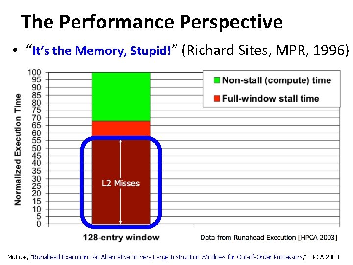
The Performance Perspective • “It’s the Memory, Stupid!” (Richard Sites, MPR, 1996) Mutlu+, “Runahead Execution: An Alternative to Very Large Instruction Windows for Out-of-Order Processors, ” HPCA 2003.

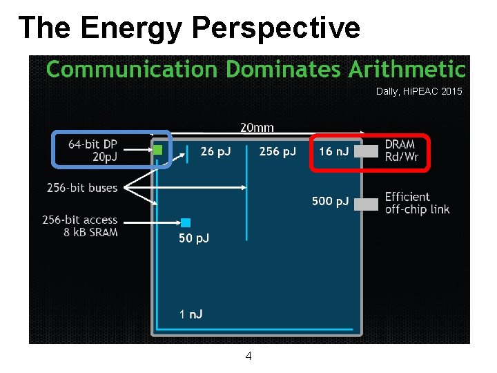
The Energy Perspective Dally, Hi. PEAC 2015 4

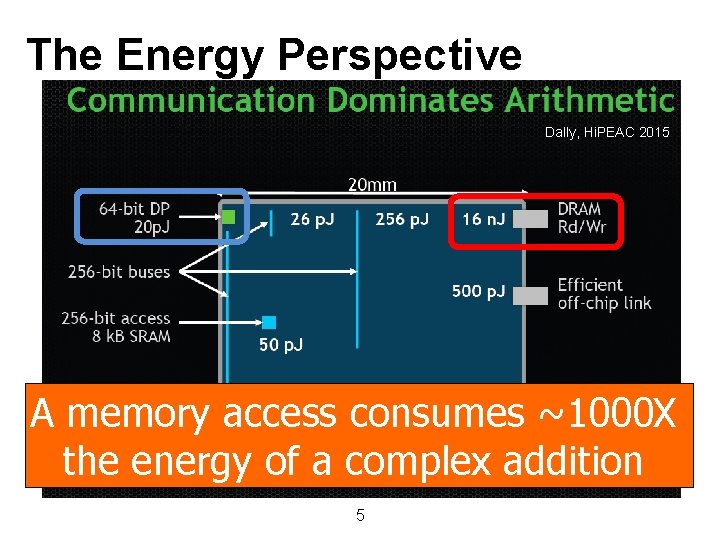
The Energy Perspective Dally, Hi. PEAC 2015 A memory access consumes ~1000 X the energy of a complex addition 5

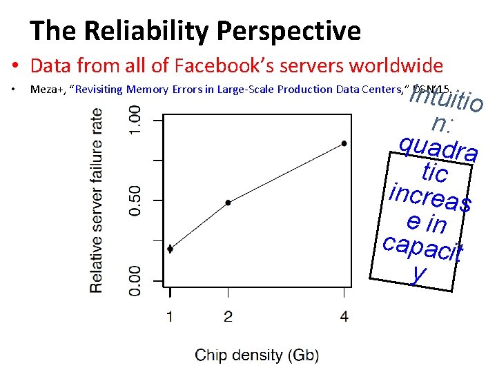
The Reliability Perspective • Data from all of Facebook’s servers worldwide • Intuitio n: quadra tic increas e in capacit y Meza+, “Revisiting Memory Errors in Large-Scale Production Data Centers, ” DSN’ 15. 6

The Security Perspective 7

Why Is DRAM So Slow?

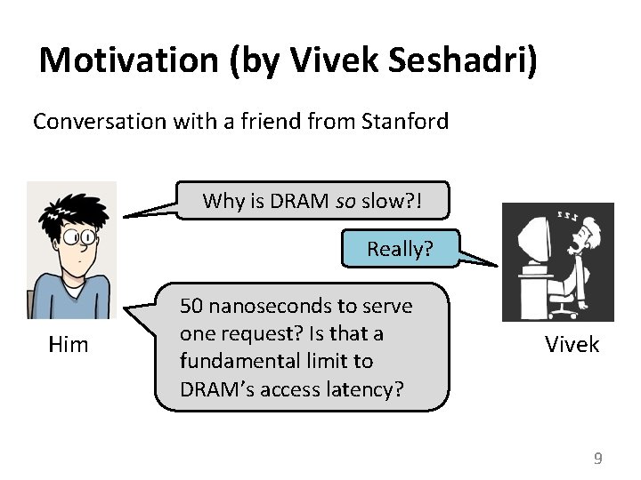
Motivation (by Vivek Seshadri) Conversation with a friend from Stanford Why is DRAM so slow? ! Really? Him 50 nanoseconds to serve one request? Is that a fundamental limit to DRAM’s access latency? Vivek 9

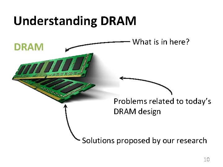
Understanding DRAM What is in here? Problems related to today’s DRAM design Solutions proposed by our research 10

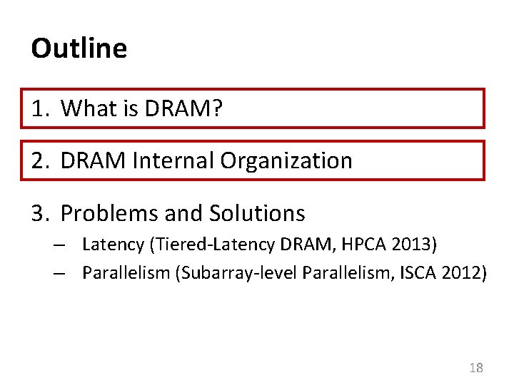
Outline 1. What is DRAM? 2. DRAM Internal Organization 3. Problems and Solutions – Latency (Tiered-Latency DRAM, HPCA 2013) – Parallelism (Subarray-level Parallelism, ISCA 2012) 11

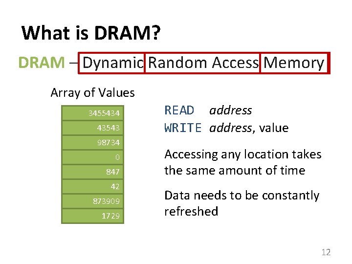
What is DRAM? DRAM – Dynamic Random Access Memory Array of Values 3455434 43543 98734 0 847 42 873909 1729 READ address WRITE address, value Accessing any location takes the same amount of time Data needs to be constantly refreshed 12

DRAM in Today’s Systems Why DRAM? Why not some other memory? 13

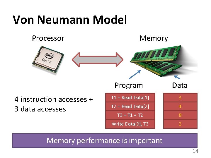
Von Neumann Model Processor 4 instruction accesses + 3 data accesses Memory Program Data T 1 = Read Data[1] 3 T 2 = Read Data[2] 4 T 3 = T 1 + T 2 8 Write Data[3], T 3 2 Memory performance is important 14

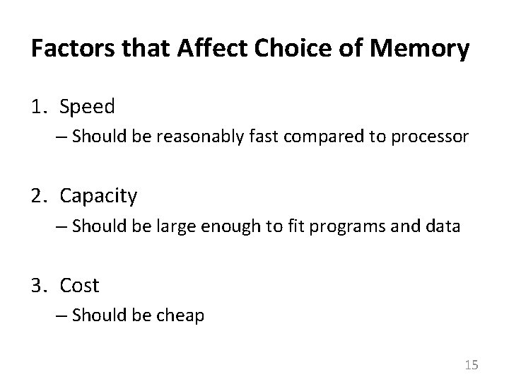
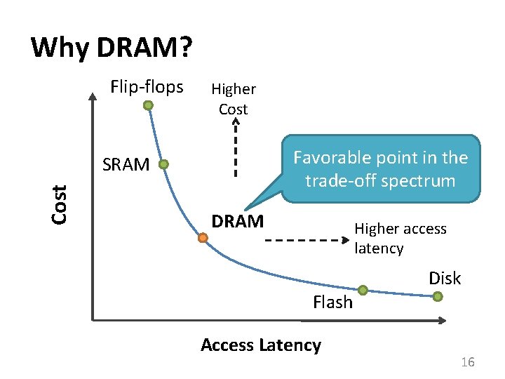
Factors that Affect Choice of Memory 1. Speed – Should be reasonably fast compared to processor 2. Capacity – Should be large enough to fit programs and data 3. Cost – Should be cheap 15

Why DRAM? Flip-flops Higher Cost Favorable point in the trade-off spectrum Cost SRAM DRAM Higher access latency Flash Access Latency Disk 16

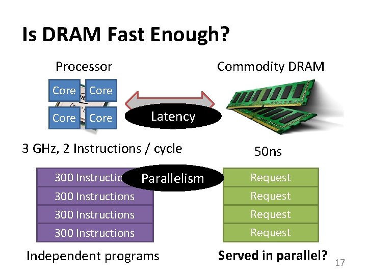
Is DRAM Fast Enough? Processor Core Commodity DRAM Latency 3 GHz, 2 Instructions / cycle 300 Instructions Parallelism 300 Instructions Independent programs 50 ns Request Served in parallel? 17

Outline 1. What is DRAM? 2. DRAM Internal Organization 3. Problems and Solutions – Latency (Tiered-Latency DRAM, HPCA 2013) – Parallelism (Subarray-level Parallelism, ISCA 2012) 18

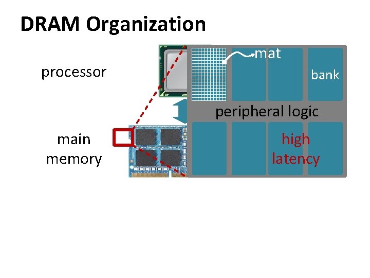
DRAM Organization processor mat bank peripheral logic main memory high latency

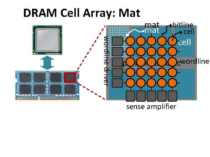
DRAM Cell Array: Mat mat wordline driver bitline cell peripheral logicwordline sense amplifier

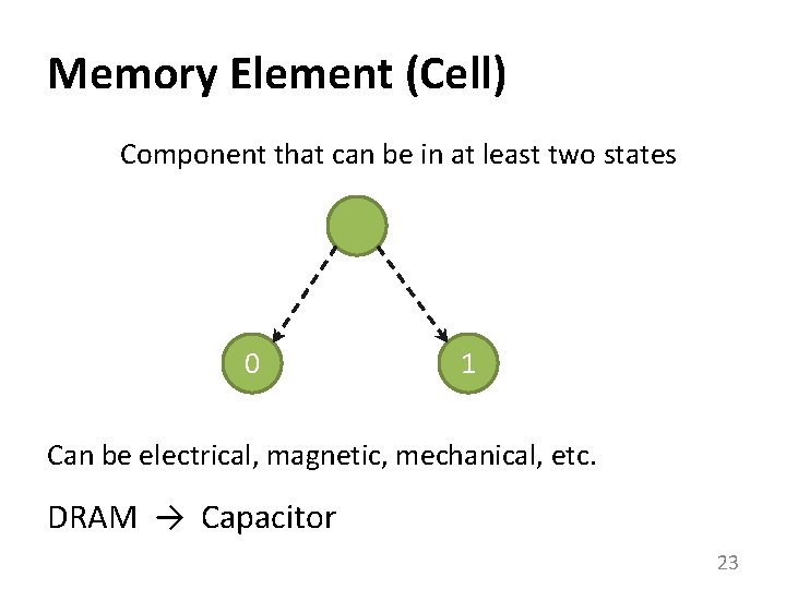
Memory Element (Cell) Component that can be in at least two states 0 1 Can be electrical, magnetic, mechanical, etc. DRAM → Capacitor 23

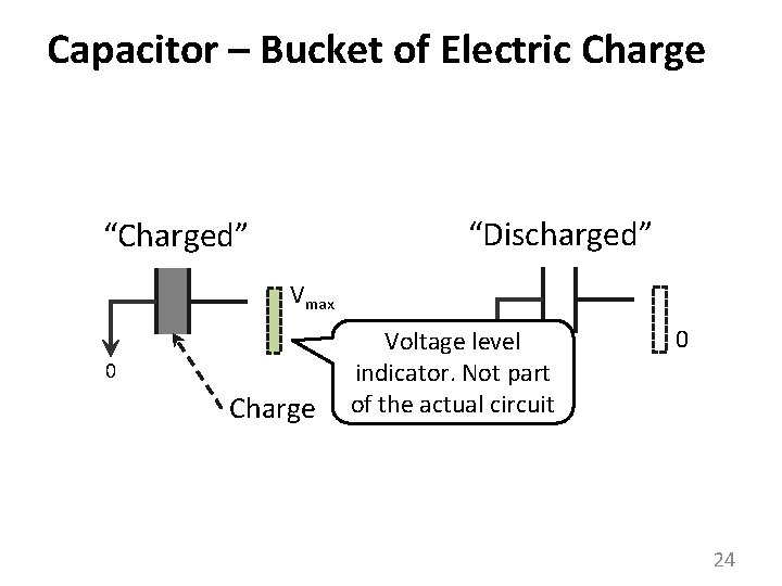
Capacitor – Bucket of Electric Charge “Discharged” “Charged” Vmax 0 Charge Voltage level 0 indicator. Not part of the actual circuit 0 24

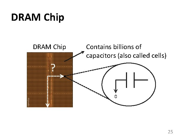
DRAM Chip Contains billions of capacitors (also called cells) ? 0 25

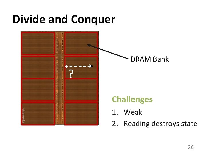
Divide and Conquer DRAM Bank ? Challenges 1. Weak 2. Reading destroys state 26

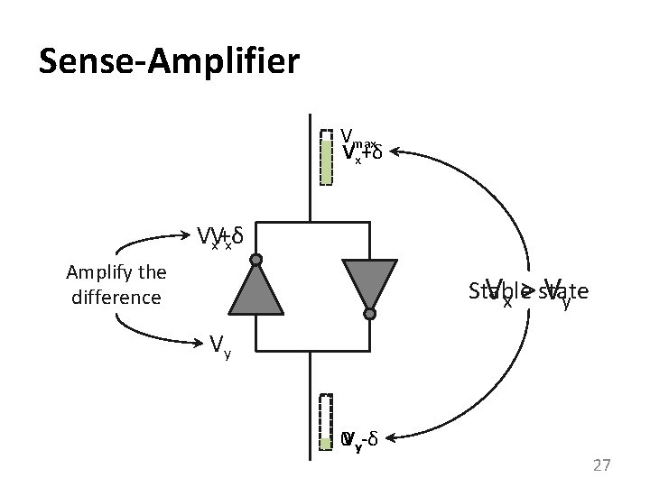
Sense-Amplifier Vmax Vx+δ VV x+δ x Amplify the difference Stable state Vx > Vy Vy 0 Vy-δ 27

Outline 1. What is DRAM? 2. DRAM Internal Organization – DRAM Cell – DRAM Array – DRAM Bank 3. Problems and Solutions – Latency (Tiered-Latency DRAM, HPCA 2013) – Parallelism (Subarray-level Parallelism, ISCA 2012) 28

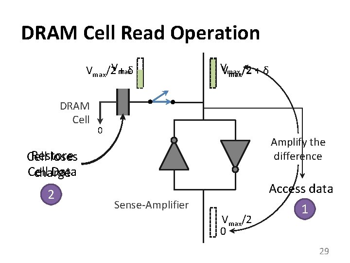
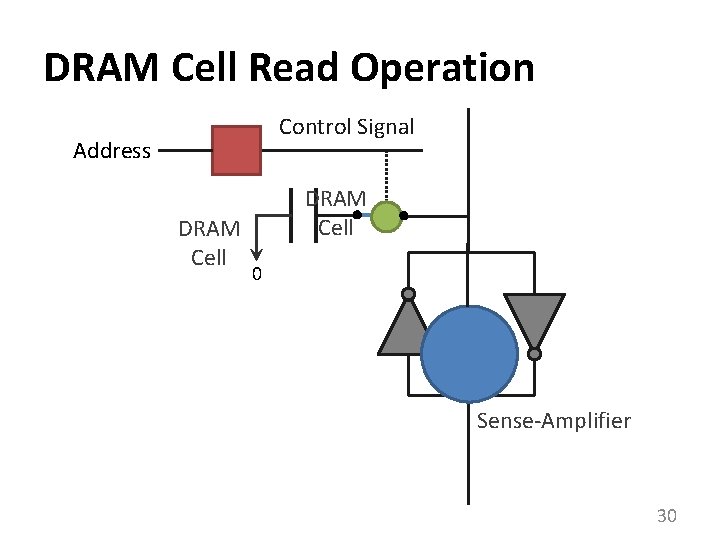
DRAM Cell Read Operation Vmax/2 + δ DRAM Cell VVmax /2 + δ max/2 0 Amplify the difference Restore Cell loses Cell Data charge 2 Access data Sense-Amplifier Vmax/2 0 1 29

DRAM Cell Read Operation Control Signal Address DRAM Cell 0 Sense-Amplifier 30

Outline 1. What is DRAM? 2. DRAM Internal Organization – DRAM Cell – DRAM Array – DRAM Bank 3. Problems and Solutions – Latency (Tiered-Latency DRAM, HPCA 2013; Adaptive-Latency DRAM, HPCA 2015) – Parallelism (Subarray-level Parallelism, ISCA 2012) 31

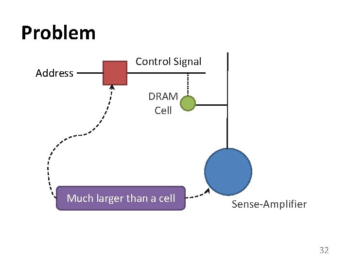
Problem Address Control Signal DRAM Cell Much larger than a cell Sense-Amplifier 32

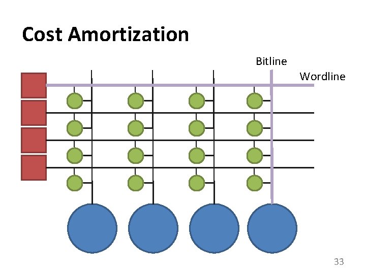
Cost Amortization Bitline Wordline 33

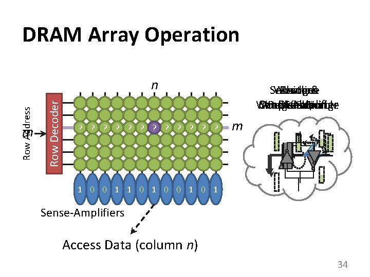
DRAM Array Operation m Row Decoder Row Address n 1? 0? 0? 1? Wordline Restore Sensing & Charge Sense-Amplifier Disable Amplification Restoration Wordline Enable Charge Sharing m ↑ ½ ½ ↑ ½ 1 ½ 0 ½ 1 ½ 0 ½ 1 ½ ↓ ↓ ½ Sense-Amplifiers Access Data (column n) 34

Outline 1. What is DRAM? 2. DRAM Internal Organization – DRAM Cell – DRAM Array – DRAM Bank 3. Problems and Solutions – Latency (Tiered-Latency DRAM, HPCA 2013 Adaptive-Latency DRAM, HPCA 2015) – Parallelism (Subarray-level Parallelism, ISCA 2012) 35

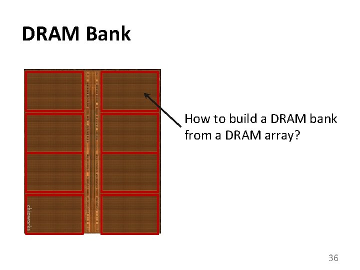
DRAM Bank How to build a DRAM bank from a DRAM array? 36

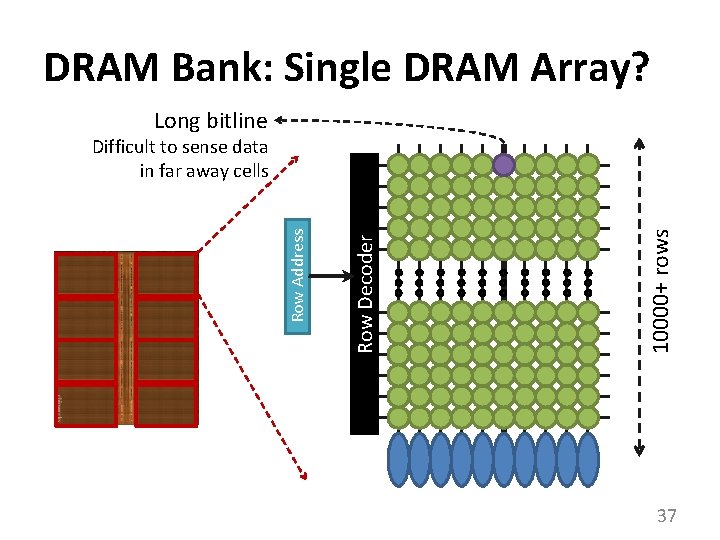
DRAM Bank: Single DRAM Array? Long bitline 1 0 0 1 10000+ rows Row Decoder Row Address Difficult to sense data in far away cells 37

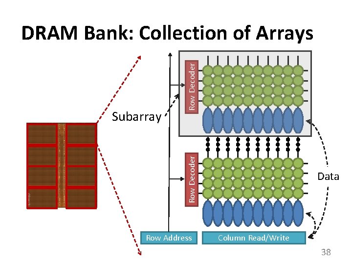
1 0 0 1 Row Decoder Subarray Row Decoder DRAM Bank: Collection of Arrays Row Address Data Column Read/Write 38

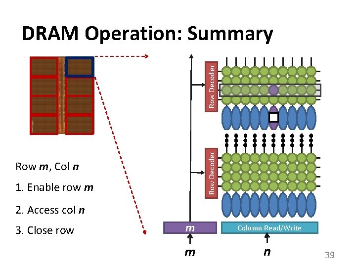
1 0 0 1 Row Decoder DRAM Operation: Summary Row m, Col n 1. Enable row m 2. Access col n 3. Close row Row Address m Column Read/Write m n 39

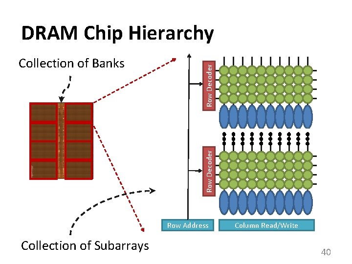
1 0 0 1 Row Decoder Collection of Banks Row Decoder DRAM Chip Hierarchy Row Address Collection of Subarrays Column Read/Write 40

Outline 1. What is DRAM? 2. DRAM Internal Organization 3. Problems and Solutions – Latency (Tiered-Latency DRAM, HPCA 2013; Adaptive-Latency DRAM, HPCA 2015) – Parallelism (Subarray-level Parallelism, ISCA 2012) 41

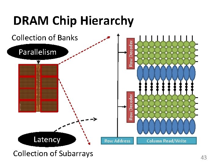
Factors That Affect Performance 1. Latency – How fast can DRAM serve a request? 2. Parallelism – How many requests can DRAM serve in parallel? 42

Collection of Banks 1 0 0 1 Row Decoder Parallelism Row Decoder DRAM Chip Hierarchy Latency Collection of Subarrays Row Address Column Read/Write 43

Outline 1. What is DRAM? 2. DRAM Internal Organization 3. Problems and Solutions – Latency (Tiered-Latency DRAM, HPCA 2013; Adaptive-Latency DRAM, HPCA 2015) – Parallelism (Subarray-level Parallelism, ISCA 2012) 44

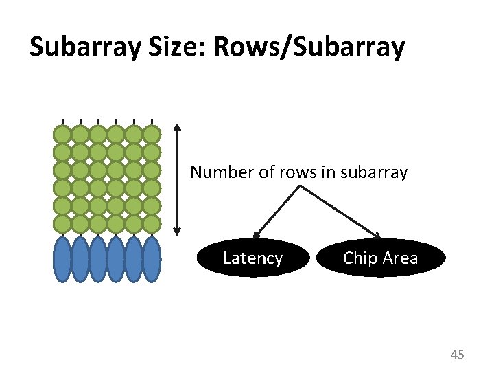
Subarray Size: Rows/Subarray Number of rows in subarray Latency Chip Area 45

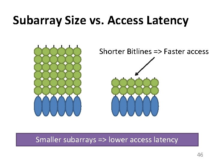
Subarray Size vs. Access Latency Shorter Bitlines => Faster access Smaller subarrays => lower access latency 46

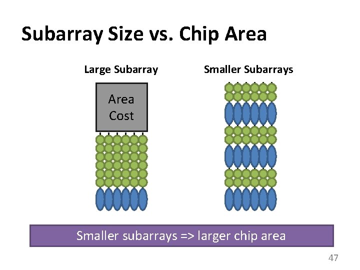
Subarray Size vs. Chip Area Large Subarray Smaller Subarrays Area Cost Smaller subarrays => larger chip area 47

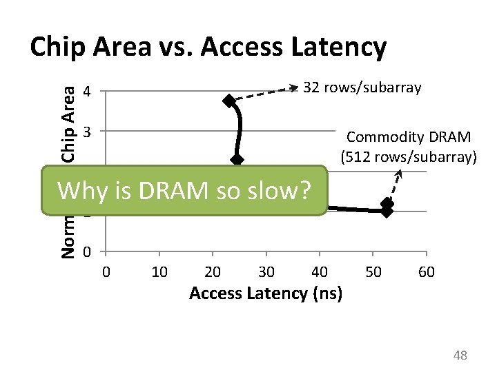
Normalized Chip Area vs. Access Latency 32 rows/subarray 4 3 Commodity DRAM (512 rows/subarray) 2 Why is DRAM so slow? 1 0 0 10 20 30 40 Access Latency (ns) 50 60 48

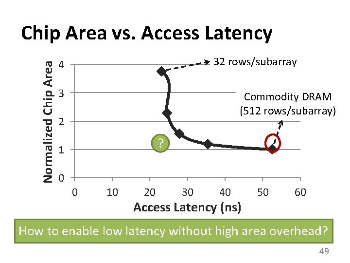
Normalized Chip Area vs. Access Latency 32 rows/subarray 4 3 Commodity DRAM (512 rows/subarray) 2 ? 1 0 0 10 20 30 40 Access Latency (ns) 50 60 How to enable low latency without high area overhead? 49

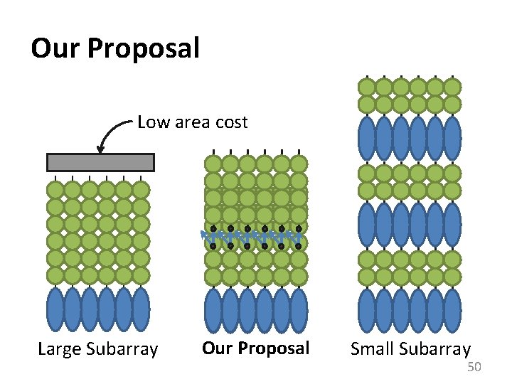
Our Proposal Low area cost Large Subarray Our Proposal Small Subarray 50

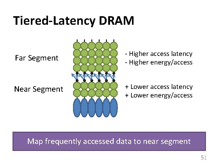
Tiered-Latency DRAM Far Segment - Higher access latency - Higher energy/access Near Segment + Lower access latency + Lower energy/access Map frequently accessed data to near segment 51

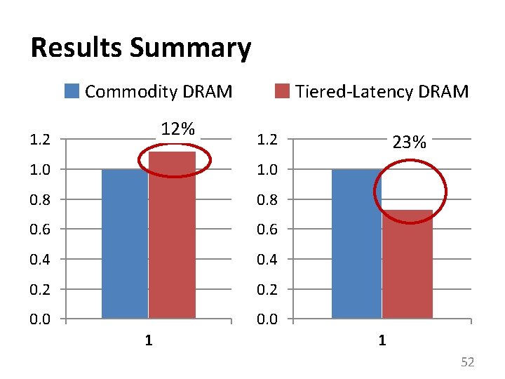
Results Summary Commodity DRAM 12% 1. 2 Tiered-Latency DRAM 1. 2 1. 0 0. 8 0. 6 0. 4 0. 2 0. 0 1 23% 1 52

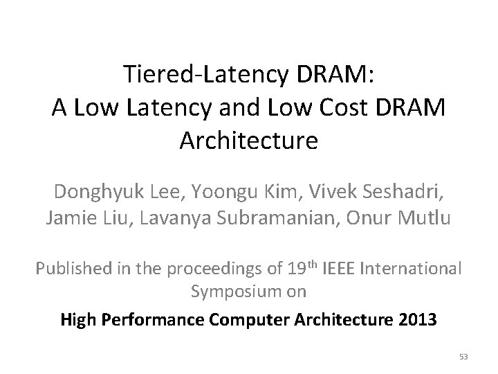
Tiered-Latency DRAM: A Low Latency and Low Cost DRAM Architecture Donghyuk Lee, Yoongu Kim, Vivek Seshadri, Jamie Liu, Lavanya Subramanian, Onur Mutlu Published in the proceedings of 19 th IEEE International Symposium on High Performance Computer Architecture 2013 53

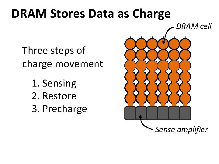
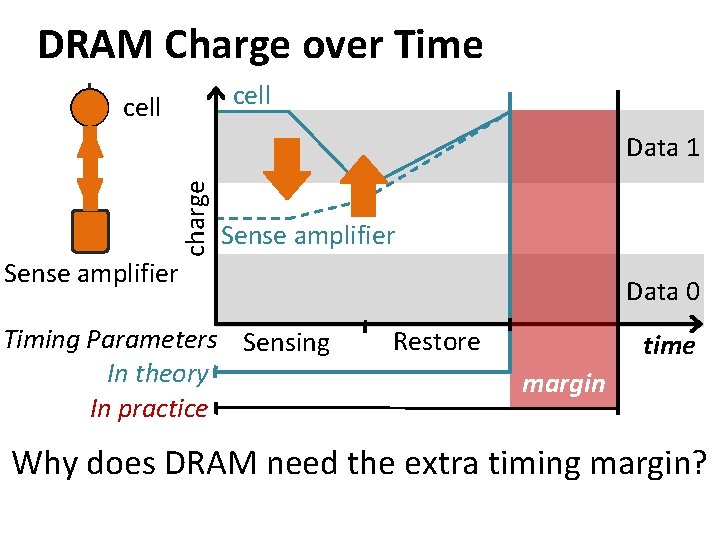
DRAM Stores Data as Charge DRAM cell Three steps of charge movement 1. Sensing 2. Restore 3. Precharge Sense amplifier

DRAM Charge over Time cell charge Data 1 Sense amplifier Timing Parameters Sensing In theory In practice Data 0 Restore time margin Why does DRAM need the extra timing margin?

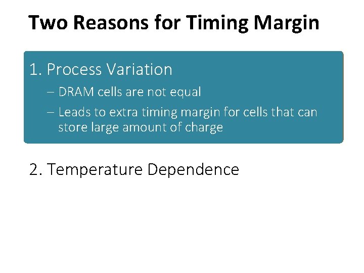
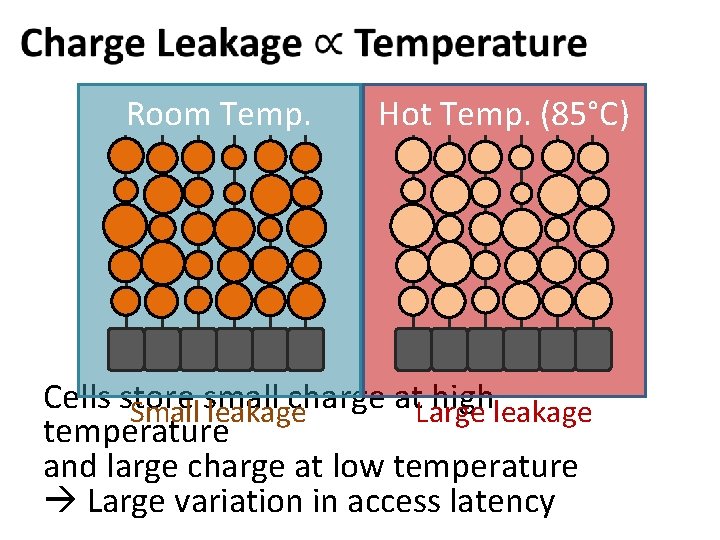
Two Reasons for Timing Margin 1. Process Variation – DRAM cells are not equal – Leads to extra timing margin for cells cell thatcan store large small amount of of charge; 2. Temperature Dependence – DRAM leaks more charge at higher temperature – Leads to extra timing margin when operating at low temperature

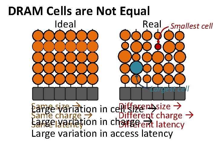
DRAM Cells are Not Equal Ideal Real Smallest cell Largest cell Same size Different size Large variation in cell size Same charge Different charge Large variation in charge Same latency Different latency Large variation in access latency

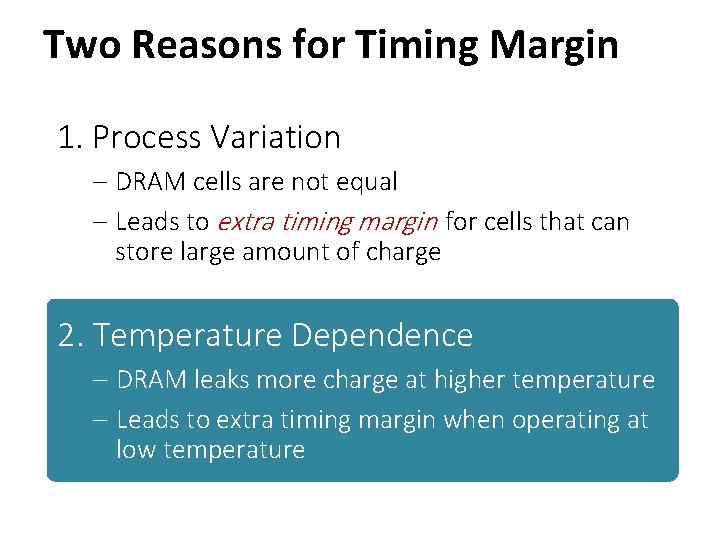
Two Reasons for Timing Margin 1. Process Variation – DRAM cells are not equal – Leads to extra timing margin for cells that can store large amount of charge 2. Temperature Dependence – DRAM leaks more charge at higher temperature – Leads to extra timing margin when operating at low temperature

Room Temp. Hot Temp. (85°C) Cells store small charge at high Small leakage Large leakage temperature and large charge at low temperature Large variation in access latency

DRAM Timing Parameters • DRAM timing parameters are dictated by the worst case – The smallest cell with the smallest charge in all DRAM products – Operating at the highest temperature • Large timing margin for the common case Can lower latency for the common case

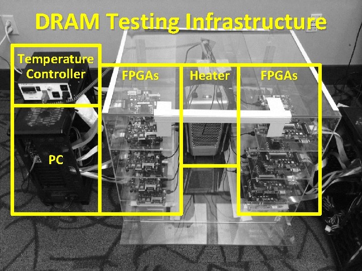
DRAM Testing Infrastructure Temperature Controller PC FPGAs Heater FPGAs

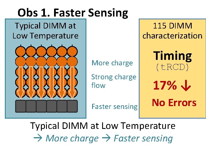
Obs 1. Faster Sensing Typical DIMM at Low Temperature 115 DIMM characterization More charge Timing (t. RCD) Strong charge flow 17% ↓ Faster sensing No Errors Typical DIMM at Low Temperature More charge Faster sensing

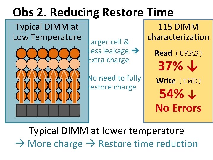
Obs 2. Reducing Restore Time Typical DIMM at Low Temperature Larger cell & 115 DIMM characterization Less leakage Extra charge Read (t. RAS) No need to fully restore charge Write (t. WR) 37% ↓ 54% ↓ No Errors Typical DIMM at lower temperature More charge Restore time reduction

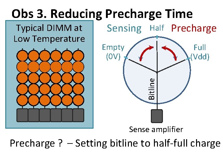
Obs 3. Reducing Precharge Time Sensing Half Precharge Empty (0 V) Full (Vdd) Bitline Typical DIMM at Low Temperature Sense amplifier Precharge ? – Setting bitline to half-full charge

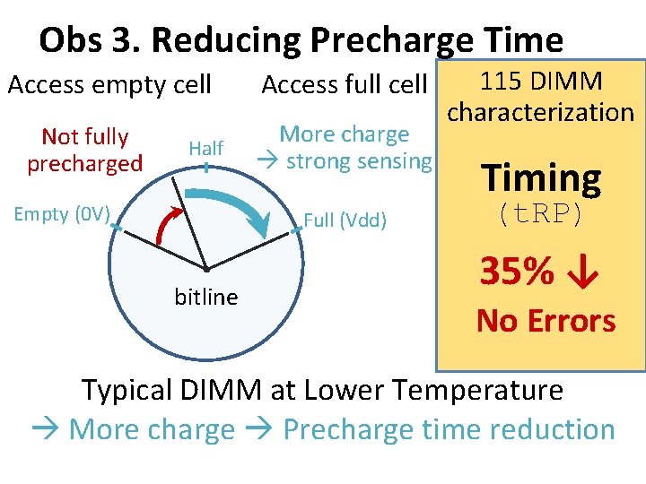
Obs 3. Reducing Precharge Time Access empty cell Not fully precharged Half Empty (0 V) Access full cell More charge strong sensing Full (Vdd) bitline 115 DIMM characterization Timing (t. RP) 35% ↓ No Errors Typical DIMM at Lower Temperature More charge Precharge time reduction

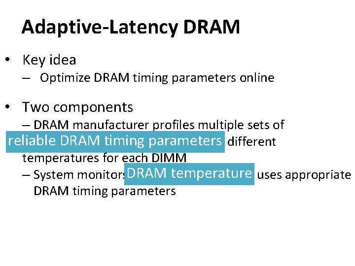
Adaptive-Latency DRAM • Key idea – Optimize DRAM timing parameters online • Two components – DRAM manufacturer profiles multiple sets of reliable DRAM timing parameters at different temperatures for each DIMM DRAM temperature – System monitors DRAM temperature & uses appropriate DRAM timing parameters

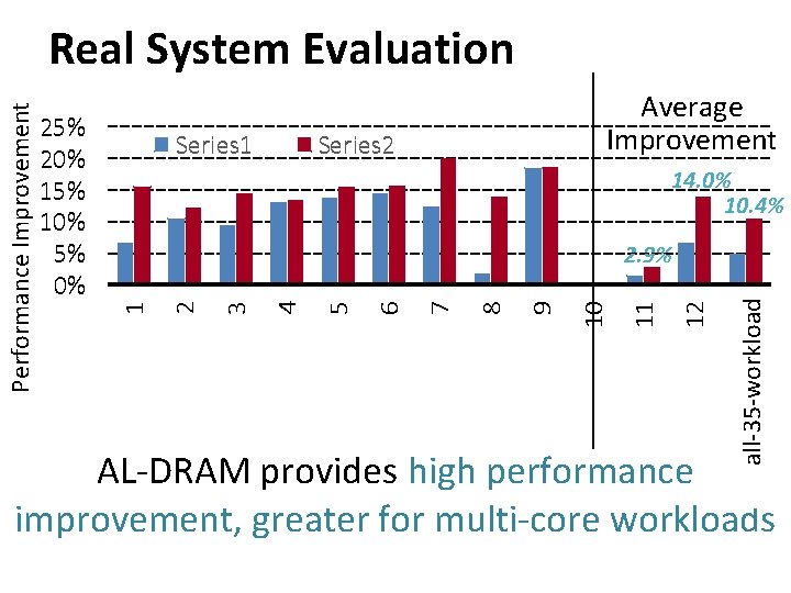
Series 1 Average Improvement Series 2 14. 0% 10. 4% 13 all-35 -workload 12 11 10 9 8 7 6 5 4 3 2. 9% 2 25% 20% 15% 10% 5% 0% 1 Performance Improvement Real System Evaluation AL-DRAM provides high performance improvement, greater for multi-core workloads

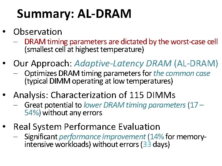
Summary: AL-DRAM • Observation – DRAM timing parameters are dictated by the worst-case cell (smallest cell at highest temperature) • Our Approach: Adaptive-Latency DRAM (AL-DRAM) – Optimizes DRAM timing parameters for the common case (typical DIMM operating at low temperatures) • Analysis: Characterization of 115 DIMMs – Great potential to lower DRAM timing parameters (17 – 54%) without any errors • Real System Performance Evaluation – Significant performance improvement (14% for memoryintensive workloads) without errors (33 days)

Adaptive-Latency DRAM: Optimizing DRAM Timing for the Common-Case Donghyuk Lee, Yoongu Kim, Gennady Pekhimenko, Samira Khan, Vivek Seshadri, Kevin Chang, and Onur Mutlu Published in the proceedings of 21 st International Symposium on High Performance Computer Architecture 2015 69

Outline 1. What is DRAM? 2. DRAM Internal Organization 3. Problems and Solutions – Latency (Tiered-Latency DRAM, HPCA 2013; Adaptive-Latency DRAM, HPCA 2015) – Parallelism (Subarray-level Parallelism, ISCA 2012) 70

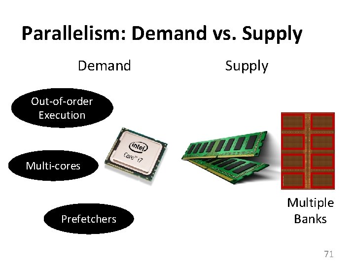
Parallelism: Demand vs. Supply Demand Supply Out-of-order Execution Multi-cores Prefetchers Multiple Banks 71

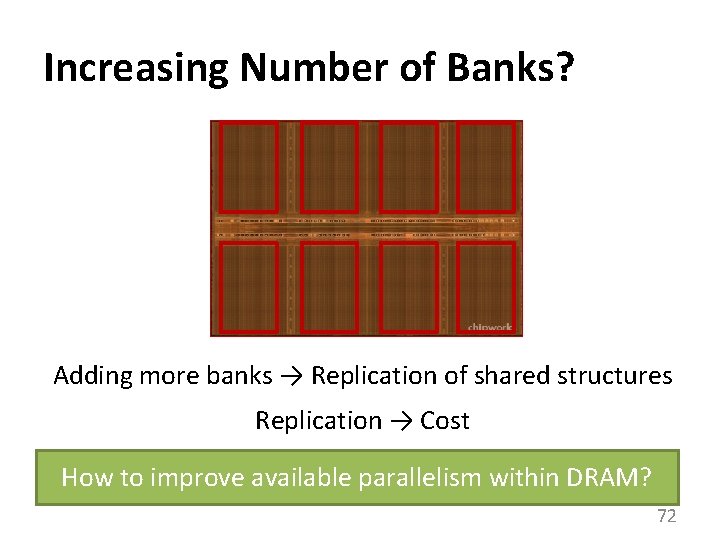
Increasing Number of Banks? Adding more banks → Replication of shared structures Replication → Cost How to improve available parallelism within DRAM? 72

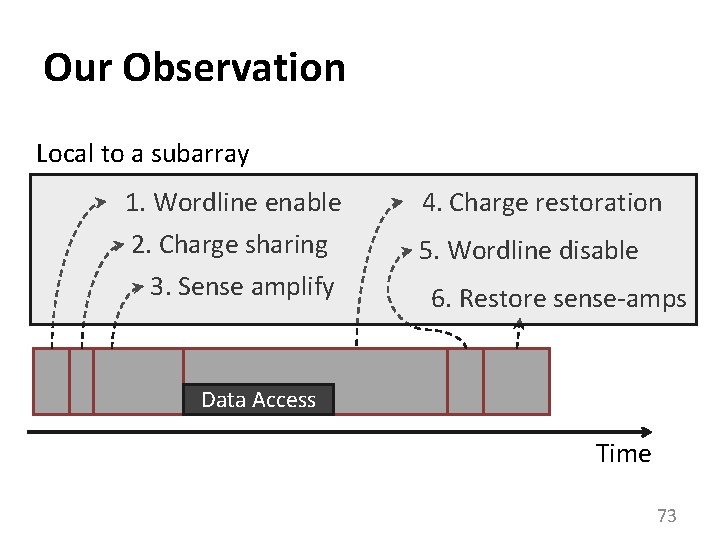
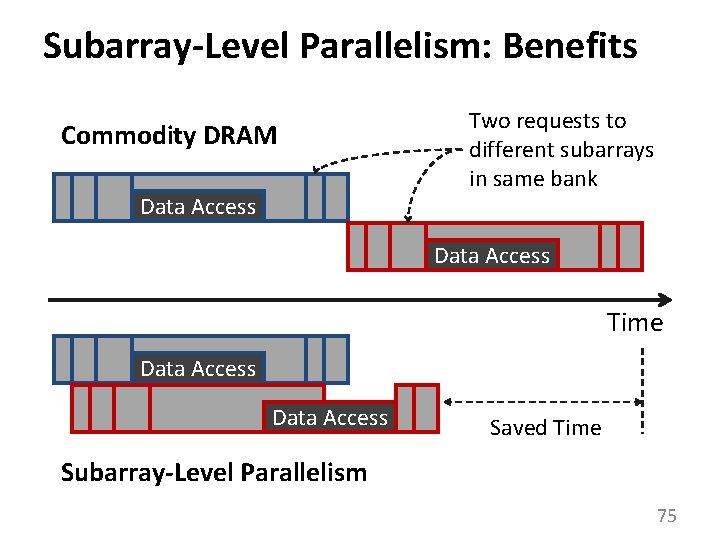
Our Observation Local to a subarray 1. Wordline enable 4. Charge restoration 2. Charge sharing 3. Sense amplify 5. Wordline disable 6. Restore sense-amps Data Access Time 73

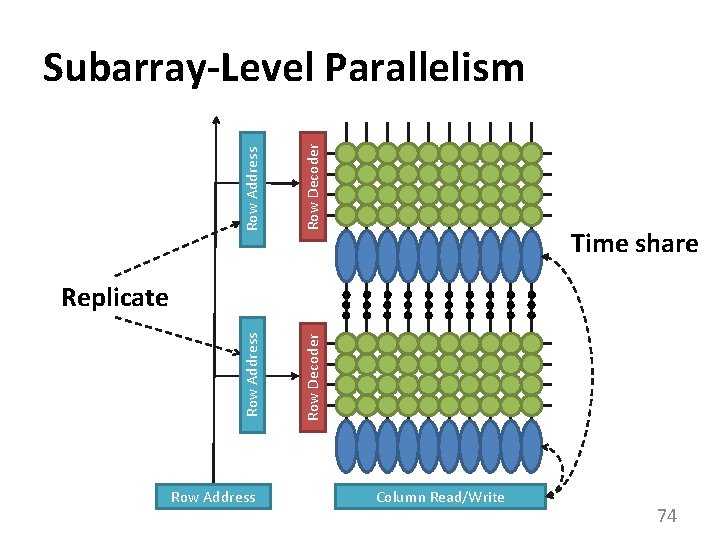
Row Address Row Decoder Subarray-Level Parallelism 1 0 0 1 Time share Replicate Row Address Column Read/Write 74

Subarray-Level Parallelism: Benefits Commodity DRAM Data Access Two requests to different subarrays in same bank Data Access Time Data Access Saved Time Subarray-Level Parallelism 75

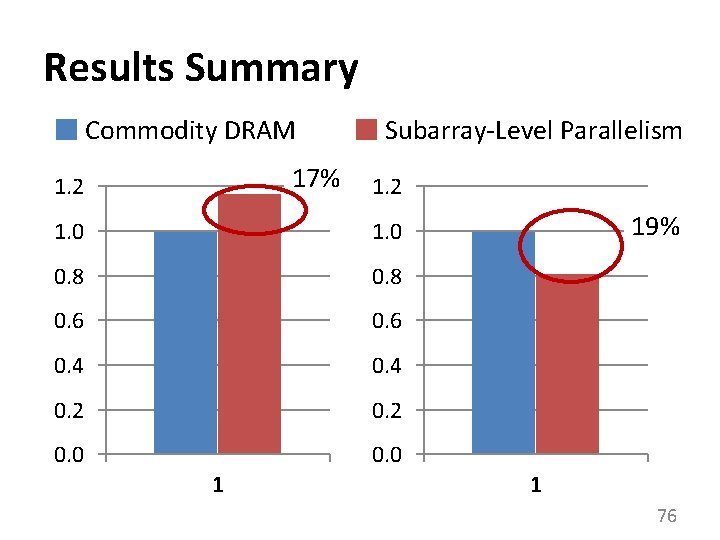
Results Summary Commodity DRAM 17% 1. 2 Subarray-Level Parallelism 1. 2 1. 0 0. 8 0. 6 0. 4 0. 2 0. 0 1 19% 1 76

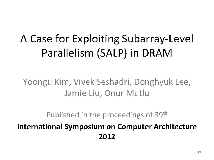
A Case for Exploiting Subarray-Level Parallelism (SALP) in DRAM Yoongu Kim, Vivek Seshadri, Donghyuk Lee, Jamie Liu, Onur Mutlu Published in the proceedings of 39 th International Symposium on Computer Architecture 2012 77

Review #5 • Row. Clone: Fast and Energy-Efficient In -DRAM Bulk Data Copy and Initialization Vivek Seshadri et al. , MICRO 2013 78

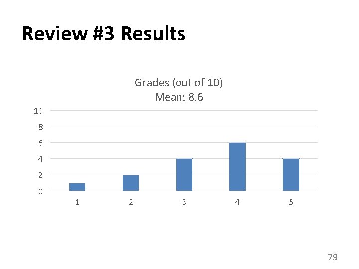
Review #3 Results Grades (out of 10) Mean: 8. 6 10 8 6 4 2 0 1 2 3 4 5 79

CSC 2231: Parallel Computer Architecture and Programming Main Memory Fundamentals Prof. Gennady Pekhimenko University of Toronto Fall 2017 The content of this lecture is adapted from the slides of Vivek Seshadri, Donghyuk Lee, Yoongu Kim, and lectures of Onur Mutlu @ ETH and CMU