CMS HCAL upgrade and its electronics Tullio Grassi
- Slides: 36

CMS HCAL upgrade and its electronics Tullio Grassi for the CMS HCAL collaboration PH/ESE group seminar CERN, 5 April 2011

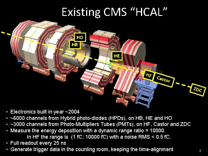
Existing CMS “HCAL” HO HB HE HF Cast or ZDC • • Electronics built in year ~2004 ~6000 channels from Hybrid photo-diodes (HPDs), on HB, HE and HO ~3000 channels from Photo-Multipliers Tubes (PMTs), on HF, Castor and ZDC Measure the energy deposition with a dynamic range ratio = 10000. In HF the range is (1 f. C; 10000 f. C) with a noise RMS < 0. 5 f. C. • Full readout every 25 ns • Generate trigger data in the counting room, keeping the time-alignment 2

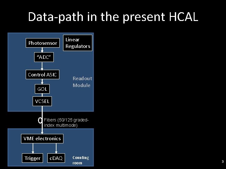
Data-path in the present HCAL Photosensor Linear Regulators “ADC” Control ASIC GOL Readout Module VCSEL Fibers (50/125 gradedindex multimode) VME electronics Trigger c. DAQ Counting room 3

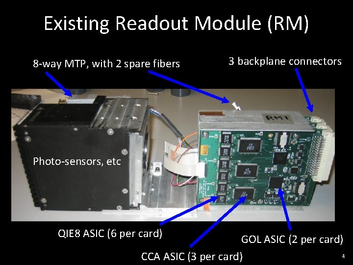
Existing Readout Module (RM) 8 -way MTP, with 2 spare fibers 3 backplane connectors Photo-sensors, etc QIE 8 ASIC (6 per card) GOL ASIC (2 per card) 4 CCA ASIC (3 per card)

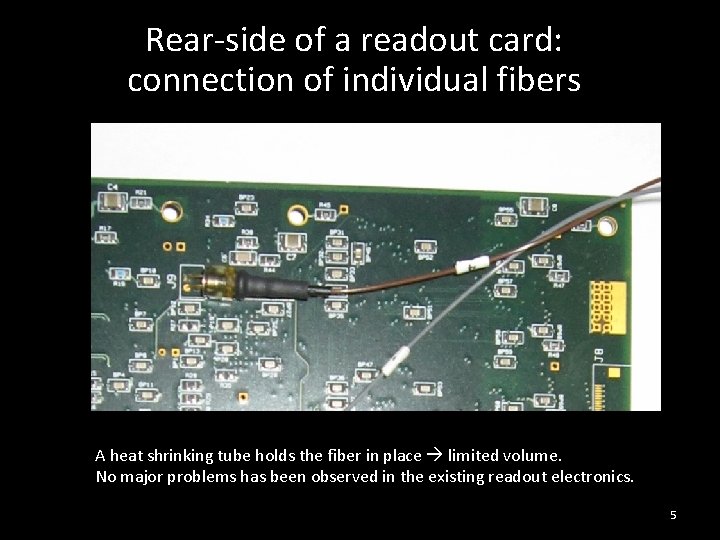
Rear-side of a readout card: connection of individual fibers A heat shrinking tube holds the fiber in place limited volume. No major problems has been observed in the existing readout electronics. 5

Upgrade: Motivations Physics: not covered in this presentation. Problems of the existing system: • • Obsolescence of electronics built in 2004 HPD: discharge; ion-feedback burst noise PMT: hit on the glass window; hit on fibers (input of PMTs) burst noise Occasional problems in the control path Improvements: • • Replace HPDs with Si. PMs Replace PMTs with multi-anode, “thin-glass” PMTs Separate readout of anodes of PMT HB, HE have 16 depths, processed together separate readout Extend the dynamic range of the analog-to-digital conversion Add TDC capabilities, in order to separate burst noise from physics signal Faster, more reliable control path 6

Upgrade: Overview Requirements: • support new photo-sensors • increase the dynamic range by a factor of 10 • increase the number of channels by a factor of 3 or 4 • add timing information (TDC) Installation and commissioning of Front-End electronics: • HB and HE: during a long shutdown after 2015 • HF: during a ~3 months technical stop Environment: • Total radiation dose = 10 krad = 100 Gy • Neutron fluence = 1013/cm 2 • Charged hadron fluence = 2 x 10¹⁰/cm 2 • Magnetic field = 4 Tesla on HB, HE. Lower field for the other partitions. Infrastructure: very limited possibilities to change power cables, optical fibers, cooling pipes, on-detector mini-crates (“Readout Boxes” a. k. a. RBX). Disclaimer : funding for the full project has not been approved yet (so far funding is allocated on a yearly basis). 7

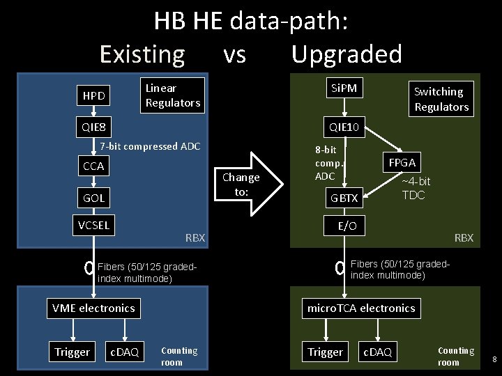
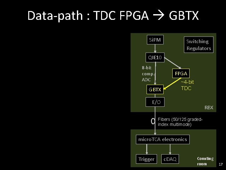
HB HE data-path: Existing vs Upgraded Linear Regulators HPD Si. PM QIE 8 QIE 10 7 -bit compressed ADC CCA Change to: GOL VCSEL RBX 8 -bit comp. ADC VME electronics c. DAQ FPGA ~4 -bit TDC GBTX E/O RBX Fibers (50/125 gradedindex multimode) Trigger Switching Regulators micro. TCA electronics Counting room Trigger c. DAQ Counting room 8

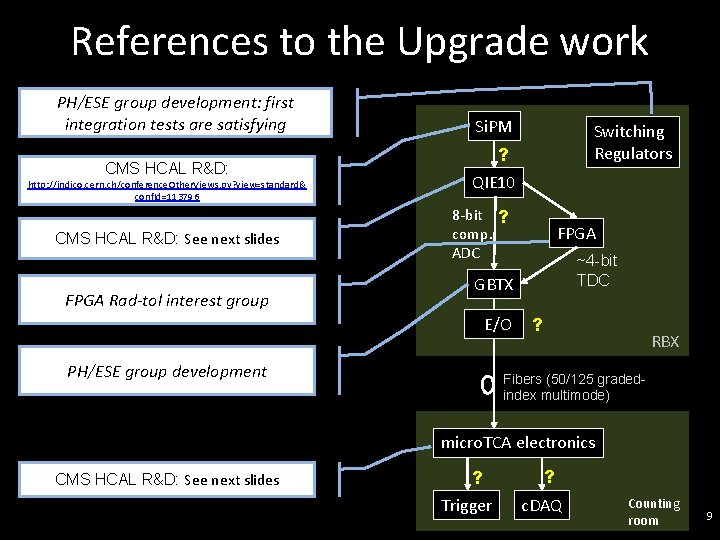
References to the Upgrade work PH/ESE group development: first integration tests are satisfying CMS HCAL R&D: http: //indico. cern. ch/conference. Other. Views. py? view=standard& conf. Id=113796 CMS HCAL R&D: See next slides FPGA Rad-tol interest group Si. PM Switching Regulators ? QIE 10 8 -bit ? comp. ADC FPGA ~4 -bit TDC GBTX E/O PH/ESE group development ? RBX Fibers (50/125 gradedindex multimode) micro. TCA electronics CMS HCAL R&D: See next slides ? Trigger ? c. DAQ Counting room 9

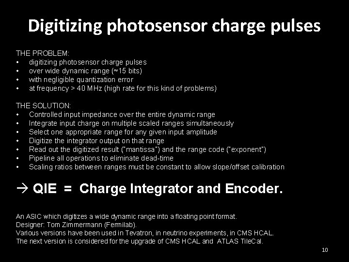
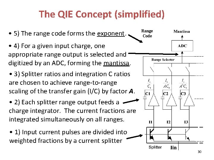
Digitizing photosensor charge pulses THE PROBLEM: • digitizing photosensor charge pulses • over wide dynamic range (≈15 bits) • with negligible quantization error • at frequency > 40 MHz (high rate for this kind of problems) THE SOLUTION: • Controlled input impedance over the entire dynamic range • Integrate input charge on multiple scaled ranges simultaneously • Select one appropriate range for any given input amplitude • Digitize the integrator output on that range • Read out the digitized result (“mantissa”) and the range code (“exponent”) • Pipeline all operations to eliminate dead-time • Scaling ratios between ranges must be constant to allow slope/offset calibration QIE = Charge Integrator and Encoder. An ASIC which digitizes a wide dynamic range into a floating point format. Designer: Tom Zimmermann (Fermilab). Various versions have been used in Tevatron, in neutrino experiments, in CMS HCAL. The next version is considered for the upgrade of CMS HCAL and ATLAS Tile. Cal. 10

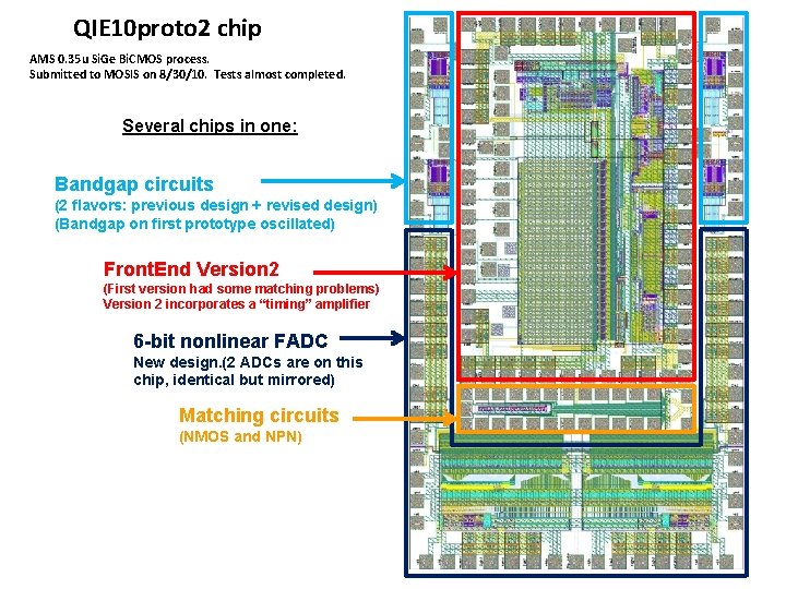
QIE 10 proto 2 chip AMS 0. 35 u Si. Ge Bi. CMOS process. Submitted to MOSIS on 8/30/10. Tests almost completed. Several chips in one: Bandgap circuits (2 flavors: previous design + revised design) (Bandgap on first prototype oscillated) Front. End Version 2 (First version had some matching problems) Version 2 incorporates a “timing” amplifier 6 -bit nonlinear FADC New design. (2 ADCs are on this chip, identical but mirrored) Matching circuits (NMOS and NPN) 11

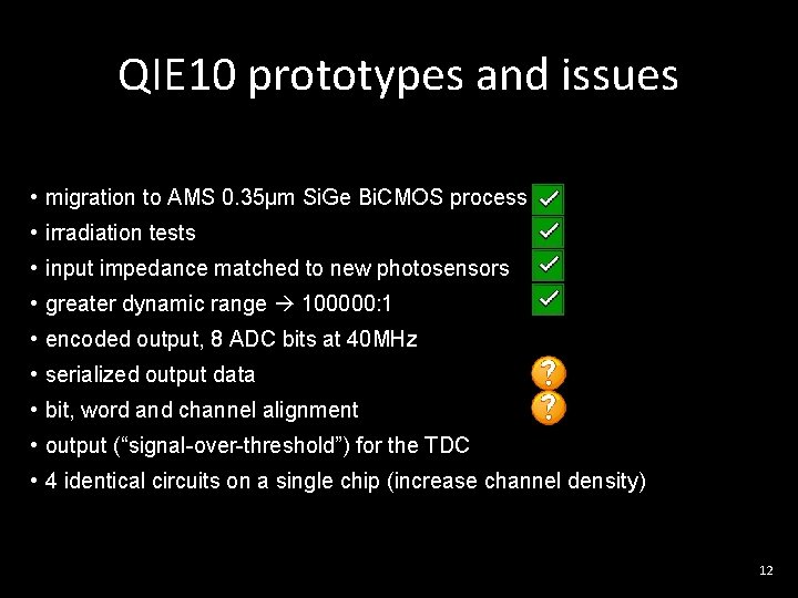
QIE 10 prototypes and issues • migration to AMS 0. 35µm Si. Ge Bi. CMOS process • irradiation tests • input impedance matched to new photosensors • greater dynamic range 100000: 1 • encoded output, 8 ADC bits at 40 MHz • serialized output data • bit, word and channel alignment • output (“signal-over-threshold”) for the TDC • 4 identical circuits on a single chip (increase channel density) 12

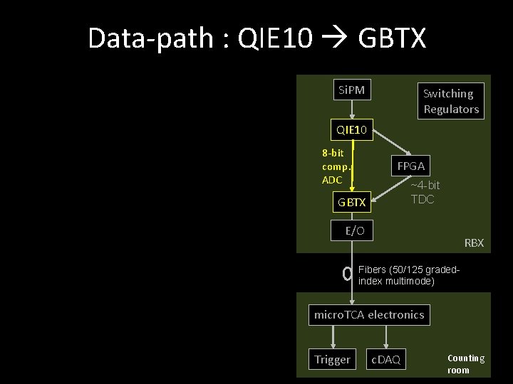
Data-path : QIE 10 GBTX Si. PM Switching Regulators QIE 10 8 -bit comp. ADC FPGA ~4 -bit TDC GBTX E/O RBX Fibers (50/125 gradedindex multimode) micro. TCA electronics Trigger c. DAQ Counting room 13

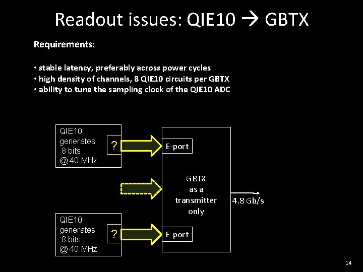
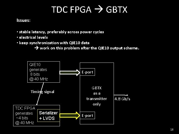
Readout issues: QIE 10 GBTX Requirements: • stable latency, preferably across power cycles • high density of channels, 8 QIE 10 circuits per GBTX • ability to tune the sampling clock of the QIE 10 ADC QIE 10 generates 8 bits @ 40 MHz ? E-port GBTX as a transmitter only ? 4. 8 Gb/s E-port 14

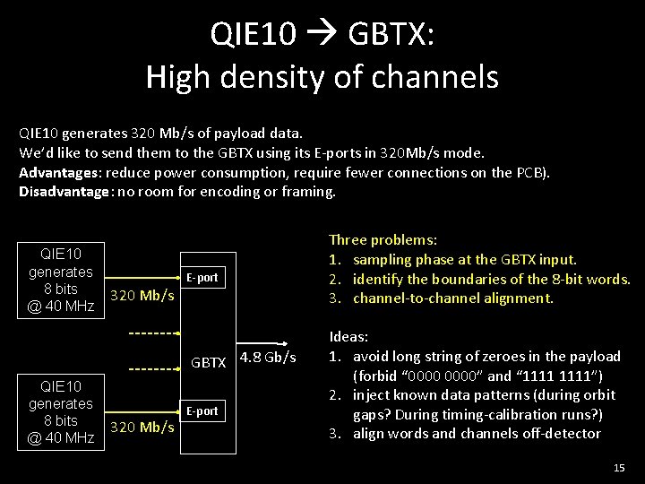
QIE 10 GBTX: High density of channels QIE 10 generates 320 Mb/s of payload data. We’d like to send them to the GBTX using its E-ports in 320 Mb/s mode. Advantages: reduce power consumption, require fewer connections on the PCB). Disadvantage: no room for encoding or framing. QIE 10 generates 8 bits @ 40 MHz 320 Mb/s E-port GBTX 4. 8 Gb/s QIE 10 generates 8 bits @ 40 MHz 320 Mb/s E-port Three problems: 1. sampling phase at the GBTX input. 2. identify the boundaries of the 8 -bit words. 3. channel-to-channel alignment. Ideas: 1. avoid long string of zeroes in the payload (forbid “ 0000” and “ 1111”) 2. inject known data patterns (during orbit gaps? During timing-calibration runs? ) 3. align words and channels off-detector 15

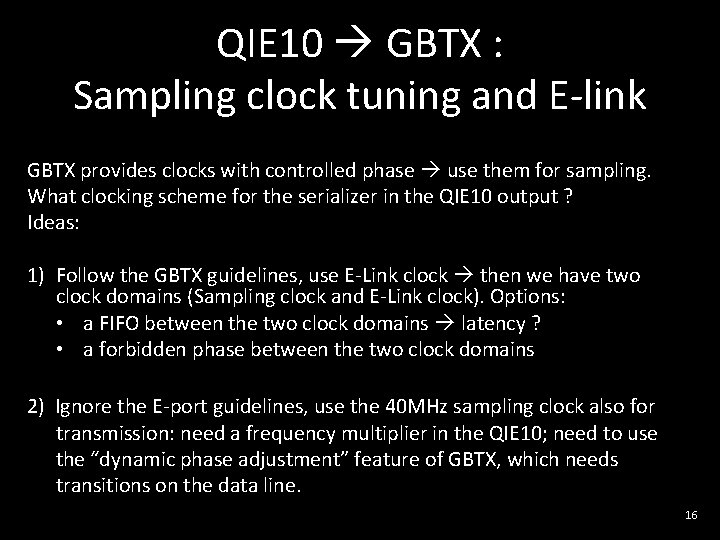
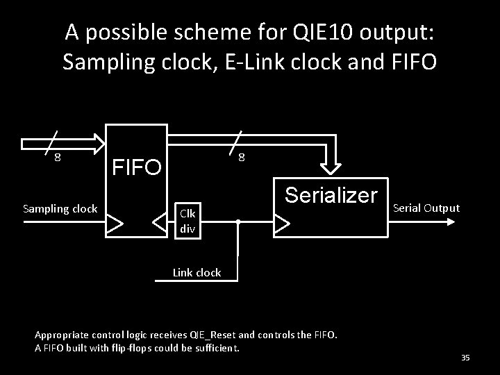
QIE 10 GBTX : Sampling clock tuning and E-link GBTX provides clocks with controlled phase use them for sampling. What clocking scheme for the serializer in the QIE 10 output ? Ideas: 1) Follow the GBTX guidelines, use E-Link clock then we have two clock domains (Sampling clock and E-Link clock). Options: • a FIFO between the two clock domains latency ? • a forbidden phase between the two clock domains 2) Ignore the E-port guidelines, use the 40 MHz sampling clock also for transmission: need a frequency multiplier in the QIE 10; need to use the “dynamic phase adjustment” feature of GBTX, which needs transitions on the data line. 16

Data-path : TDC FPGA GBTX Si. PM Switching Regulators QIE 10 8 -bit comp. ADC FPGA ~4 -bit TDC GBTX E/O RBX Fibers (50/125 gradedindex multimode) micro. TCA electronics Trigger c. DAQ Counting room 17 17

TDC FPGA GBTX Issues: • stable latency, preferably across power cycles • electrical levels • keep synchronization with QIE 10 data work on this problem after the QIE 10 output scheme. QIE 10 generates 8 bits @ 40 MHz Timing signal TDC FPGA Serializer generates ~4 bits + LVDS @ 40 MHz E-port GBTX as a transmitter only 4. 8 Gb/s E-port 18

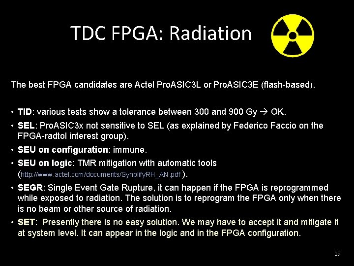
TDC FPGA: Radiation The best FPGA candidates are Actel Pro. ASIC 3 L or Pro. ASIC 3 E (flash-based). • TID: various tests show a tolerance between 300 and 900 Gy OK. • SEL: Pro. ASIC 3 x not sensitive to SEL (as explained by Federico Faccio on the FPGA-radtol interest group). • SEU on configuration: immune. • SEU on logic: TMR mitigation with automatic tools (http: //www. actel. com/documents/Synplify. RH_AN. pdf ). • SEGR: Single Event Gate Rupture, it can happen if the FPGA is reprogrammed while exposed to radiation. The solution is to reprogram the FPGA only when there is no beam or other source of radiation. • SET: Presently there is no easy solution. We may have to accept it and mitigate it at system level. It can appear in the logic and in the FPGA configuration. 19

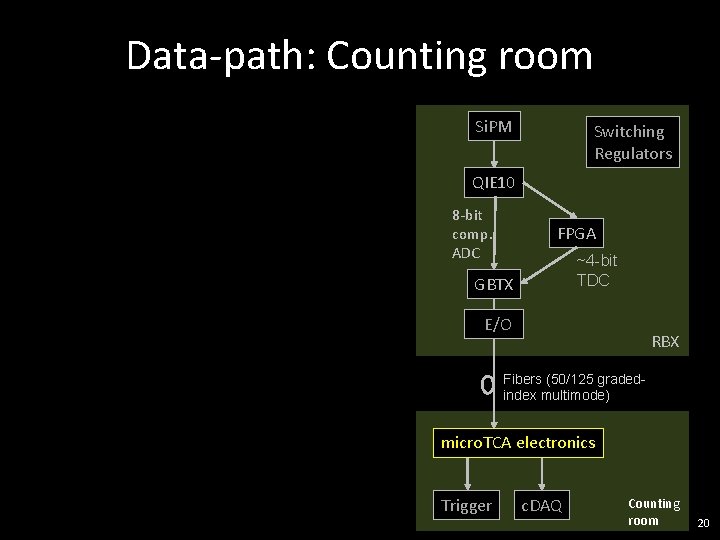
Data-path: Counting room Si. PM Switching Regulators QIE 10 8 -bit comp. ADC FPGA ~4 -bit TDC GBTX E/O RBX Fibers (50/125 gradedindex multimode) micro. TCA electronics Trigger c. DAQ Counting room 20 20

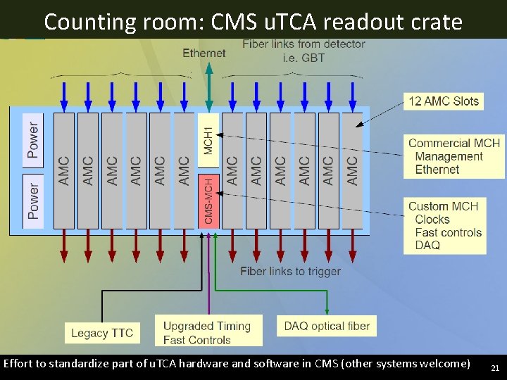
Counting room: CMS u. TCA readout crate Effort to standardize part of u. TCA hardware and software in CMS (other systems welcome) 21

Control system 22

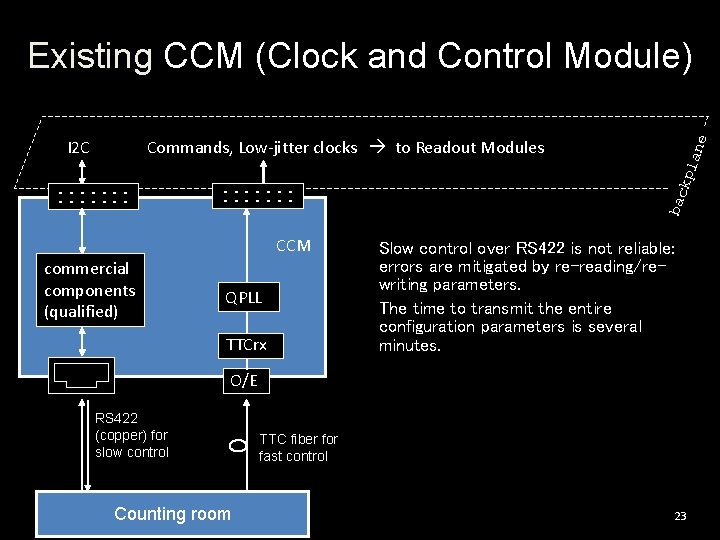
Existing CCM (Clock and Control Module) . . . CCM commercial components (qualified) QPLL TTCrx kpl . . . ane Commands, Low-jitter clocks to Readout Modules bac I 2 C Slow control over RS 422 is not reliable: errors are mitigated by re-reading/rewriting parameters. The time to transmit the entire configuration parameters is several minutes. O/E RS 422 (copper) for slow control Counting room TTC fiber for fast control 23

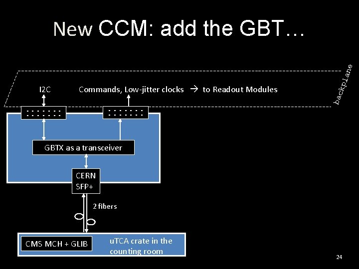
Commands, Low-jitter clocks to Readout Modules. . . . bac I 2 C kpl ane New CCM: add the GBT… GBTX as a transceiver CERN SFP+ 2 fibers CMS MCH + GLIB u. TCA crate in the counting room 24

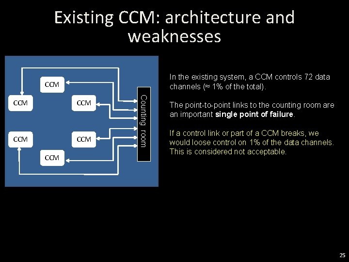
Existing CCM: architecture and weaknesses In the existing system, a CCM controls 72 data channels (≈ 1% of the total). CCM CCM CCM Counting room CCM The point-to-point links to the counting room are an important single point of failure. If a control link or part of a CCM breaks, we would loose control on 1% of the data channels. This is considered not acceptable. 25

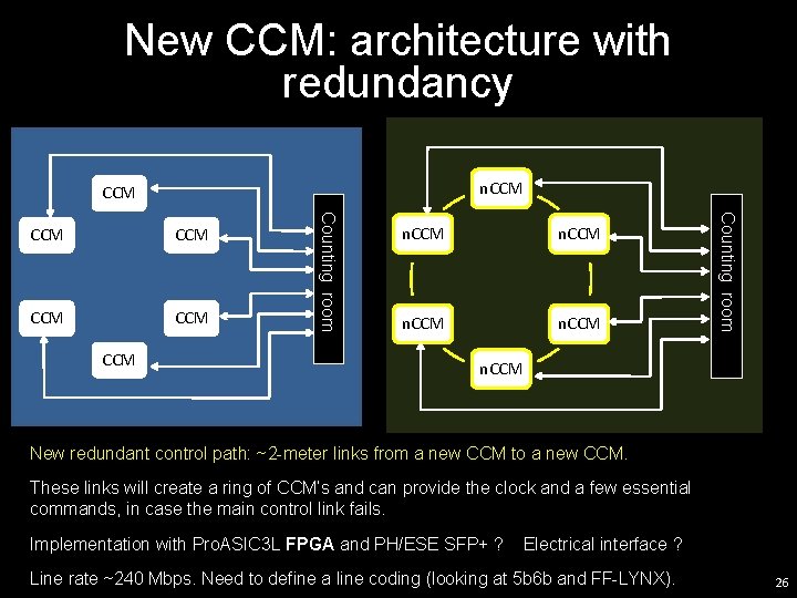
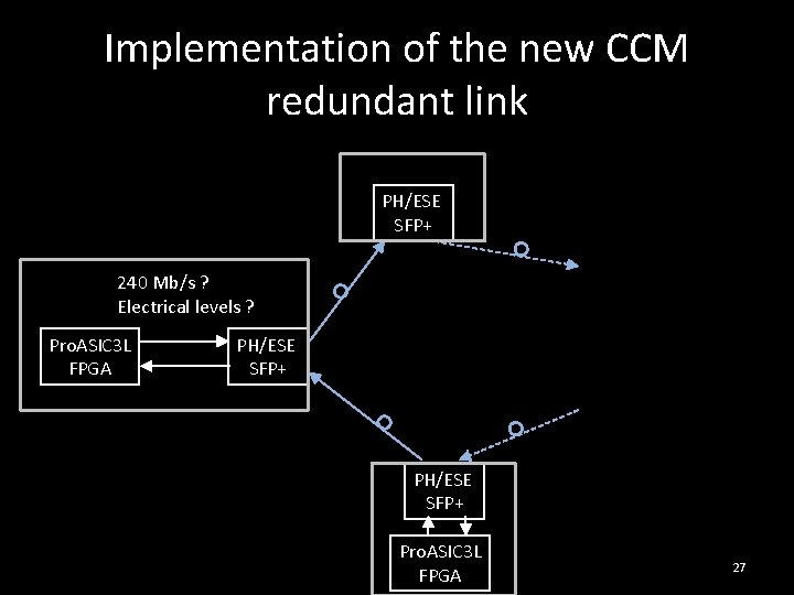
New CCM: architecture with redundancy n. CCM CCM CCM n. CCM Counting room CCM n. CCM New redundant control path: ~2 -meter links from a new CCM to a new CCM. These links will create a ring of CCM’s and can provide the clock and a few essential commands, in case the main control link fails. Implementation with Pro. ASIC 3 L FPGA and PH/ESE SFP+ ? Electrical interface ? Line rate ~240 Mbps. Need to define a line coding (looking at 5 b 6 b and FF-LYNX). 26

Implementation of the new CCM redundant link PH/ESE SFP+ 240 Mb/s ? Electrical levels ? Pro. ASIC 3 L FPGA PH/ESE SFP+ Pro. ASIC 3 L FPGA 27

Questions ? 28

Backup slides 29

The QIE Concept (simplified) • 5) The range code forms the exponent. Range Code • 4) For a given input charge, one appropriate range output is selected and digitized by an ADC, forming the mantissa. • 3) Splitter ratios and integration C ratios are chosen to achieve range-to-range scaling of the transfer gain (I/C) by factor A. • 2) Each splitter range output feeds a charge integrator. The current fractions are integrated simultaneously on all ranges. • 1) Input current pulses are divided into weighted fractions by a current splitter 30

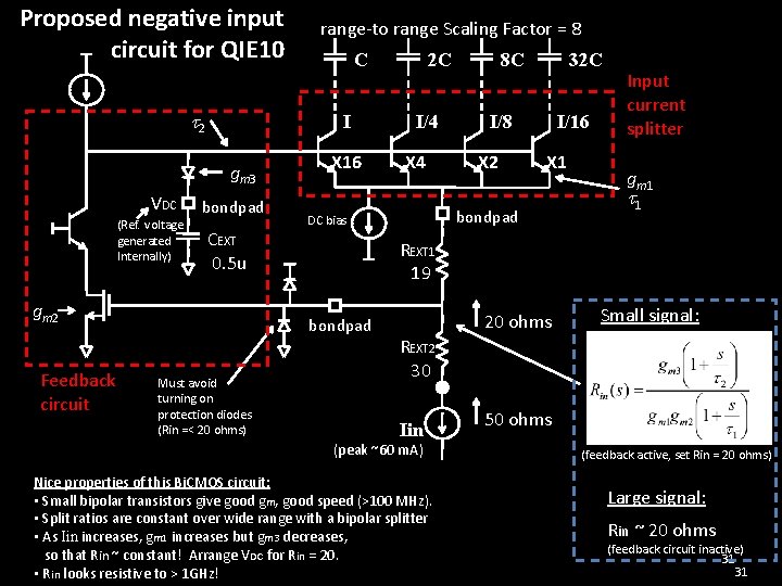
Proposed negative input circuit for QIE 10 2 (Ref. voltage generated Internally) bondpad CEXT 0. 5 u gm 2 Feedback circuit C I gm 3 VDC range-to range Scaling Factor = 8 X 16 I/4 X 4 8 C 32 C I/8 X 2 I/16 X 1 bondpad DC bias Input current splitter gm 1 1 REXT 1 19 bondpad Must avoid turning on protection diodes (Rin =< 20 ohms) 2 C 20 ohms Small signal: REXT 2 30 Iin (peak ~60 m. A) Nice properties of this Bi. CMOS circuit: • Small bipolar transistors give good gm, good speed (>100 MHz). • Split ratios are constant over wide range with a bipolar splitter • As Iin increases, gm 1 increases but gm 3 decreases, so that Rin ~ constant! Arrange VDC for Rin = 20. • Rin looks resistive to > 1 GHz! 50 ohms (feedback active, set Rin = 20 ohms) Large signal: Rin ~ 20 ohms (feedback circuit inactive) 31 31

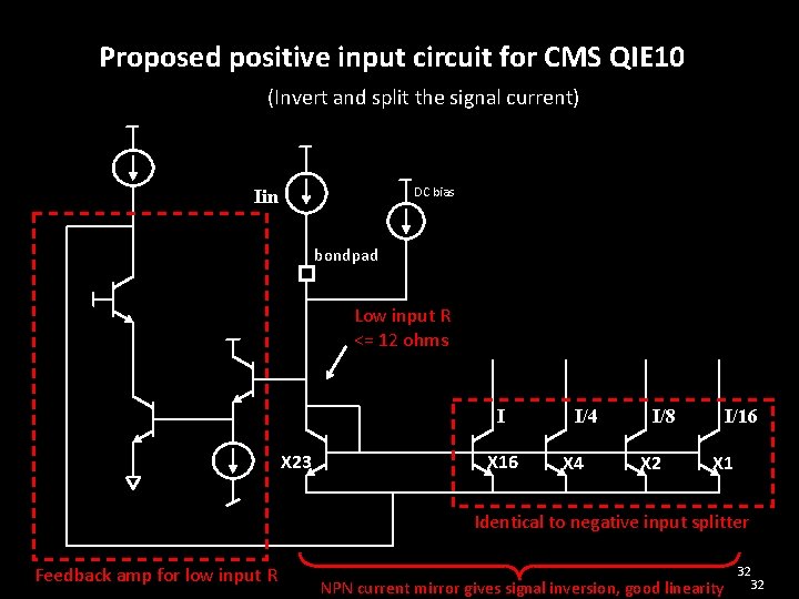
Proposed positive input circuit for CMS QIE 10 (Invert and split the signal current) DC bias Iin bondpad Low input R <= 12 ohms I X 23 X 16 I/4 X 4 I/8 X 2 I/16 X 1 Identical to negative input splitter Feedback amp for low input R NPN current mirror gives signal inversion, good linearity 32 32

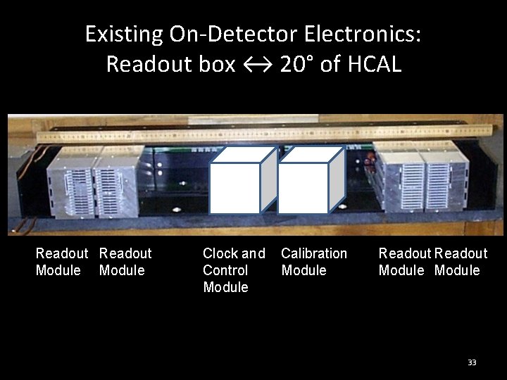
Existing On-Detector Electronics: Readout box ↔ 20° of HCAL Readout Module Clock and Control Module Calibration Module Readout Module 33

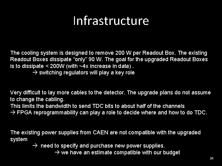
Infrastructure The cooling system is designed to remove 200 W per Readout Box. The existing Readout Boxes dissipate “only” 90 W. The goal for the upgraded Readout Boxes is to dissipate < 200 W (with ~4 x increase in data). switching regulators will play a key role Very difficult to lay more cables to the detector. The upgrade plans do not assume to change the cabling. This limits the bandwidth to send TDC bits to about half of the channels FPGA reprogrammability can play a role to decide where and how to do TDC. The existing power supplies from CAEN are not compatible with the upgraded system need to specify and purchase new power supplies. we have an estimate compatible with our budget 34

A possible scheme for QIE 10 output: Sampling clock, E-Link clock and FIFO 8 Sampling clock 8 FIFO Clk div Serializer Serial Output Link clock Appropriate control logic receives QIE_Reset and controls the FIFO. A FIFO built with flip-flops could be sufficient. 35

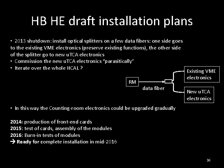
HB HE draft installation plans • 2013 shutdown: install optical splitters on a few data fibers: one side goes to the existing VME electronics (preserve existing functions), the other side of the splitter go to new u. TCA electronics • Commission the new u. TCA electronics “parasitically” • Iterate over the whole HCAL ? RM data fiber Existing VME electronics New u. TCA electronics • In this way the Counting-room electronics could be upgraded gradually 2014: production of front-end cards 2015: test of cards, assembly of the modules 2016: Burn-in tests of modules Ready for complete installation in mid-2016 36