The Trigger System Marco Grassi INFN Pisa Apr
- Slides: 33

The Trigger System Marco Grassi INFN - Pisa - Apr. 28 th, 2003 1

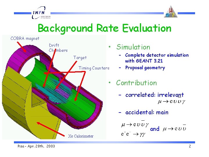
Background Rate Evaluation COBRA magnet • Simulation Drift Chambers Target Timing Counters – Complete detector simulation with GEANT 3. 21 – Proposal geometry • Contribution – correlated: irrelevant – accidental: main and Xe Calorimeter Pisa - Apr. 28 th, 2003 2

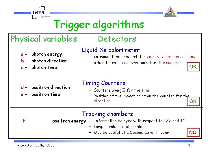
Trigger algorithms Physical variables a - photon energy b - photon direction c - photon time d - positron direction e - positron time f- Detectors Liquid Xe calorimeter – entrance face : needed for energy, direction and time – other faces : relevant only for the energy OK Timing Counters – Counters along Z for the time – Position of the impact point on the counter for the direction OK Tracking chambers positron energy – Information delayed with respect to LXe and TC Pisa - Apr. 28 th, 2003 – Large number of channels – May be useful at a Second Level trigger NO 3

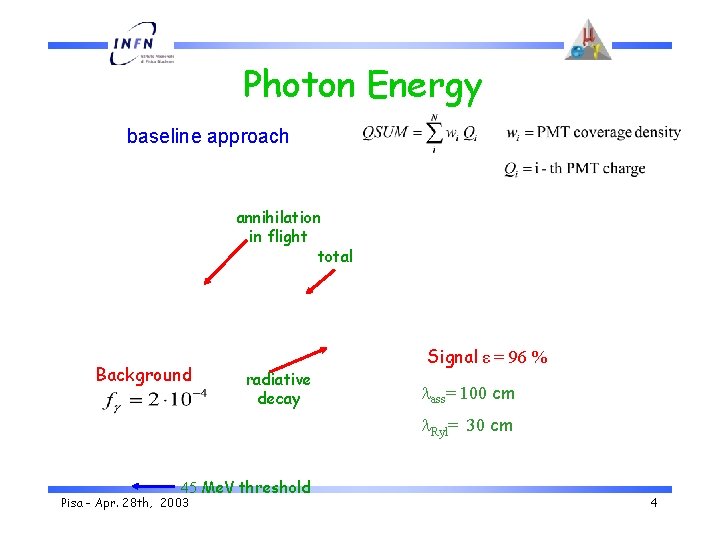
Photon Energy baseline approach annihilation in flight total Background radiative decay Signal ε = 96 % ass= 100 cm Ryl= 30 cm 45 Me. V threshold Pisa - Apr. 28 th, 2003 4

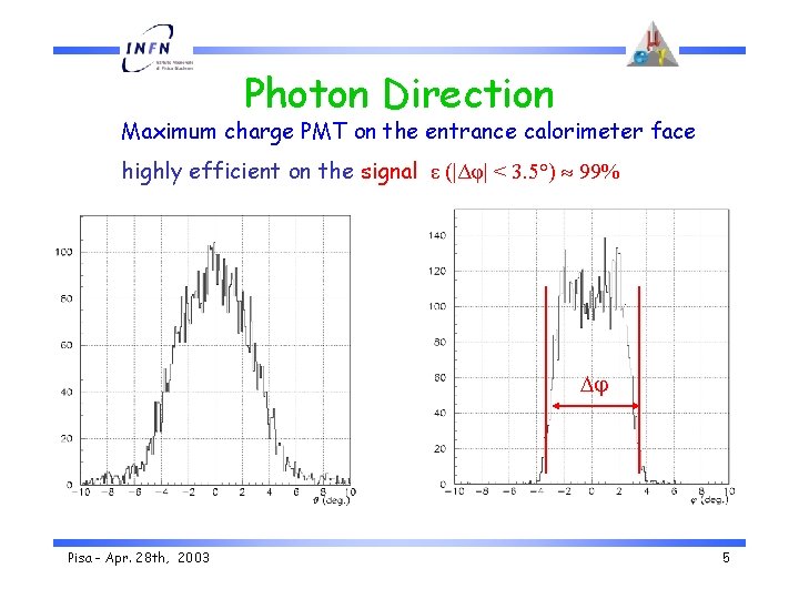
Photon Direction Maximum charge PMT on the entrance calorimeter face highly efficient on the signal ε (|Δφ| < 3. 5°) 99% Pisa - Apr. 28 th, 2003 5

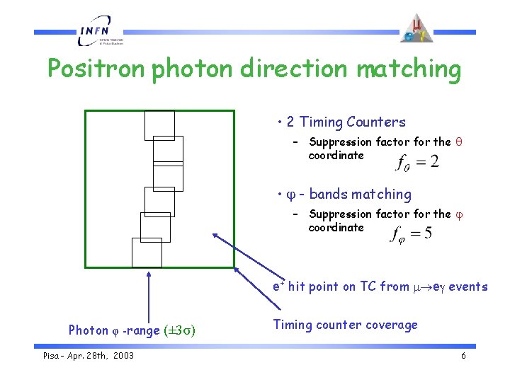
Positron photon direction matching • 2 Timing Counters – Suppression factor for the coordinate • - bands matching – Suppression factor for the coordinate e+ hit point on TC from e events Photon φ -range (± 3σ) Pisa - Apr. 28 th, 2003 Timing counter coverage 6

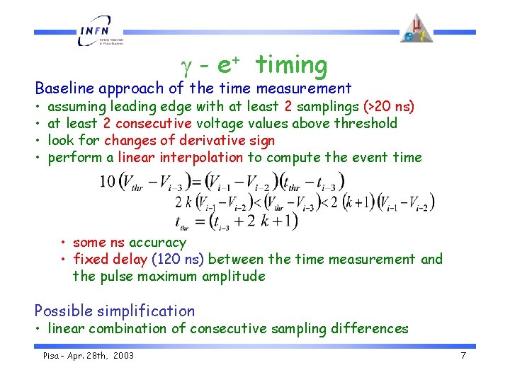
- e+ timing Baseline approach of the time measurement • • assuming leading edge with at least 2 samplings (>20 ns) at least 2 consecutive voltage values above threshold look for changes of derivative sign perform a linear interpolation to compute the event time • some ns accuracy • fixed delay (120 ns) between the time measurement and the pulse maximum amplitude Possible simplification • linear combination of consecutive sampling differences Pisa - Apr. 28 th, 2003 7

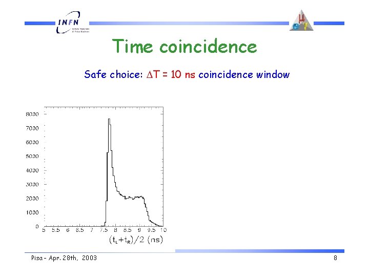
Time coincidence Safe choice: T = 10 ns coincidence window Pisa - Apr. 28 th, 2003 8

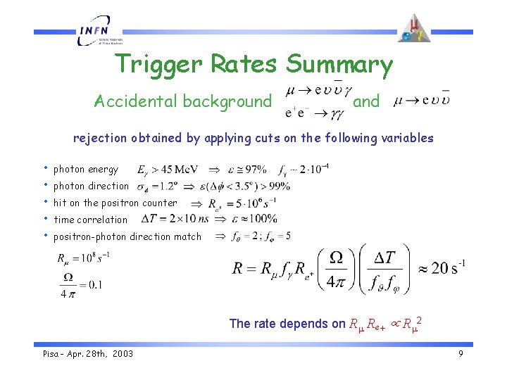
Trigger Rates Summary Accidental background and rejection obtained by applying cuts on the following variables • • • photon energy photon direction hit on the positron counter time correlation positron-photon direction match The rate depends on R Re+ R 2 Pisa - Apr. 28 th, 2003 9

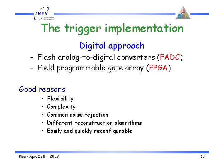
The trigger implementation Digital approach – Flash analog-to-digital converters (FADC) – Field programmable gate array (FPGA) Good reasons • • • Flexibility Complexity Common noise rejection Different reconstruction algorithms Easily and quickly reconfigurable Pisa - Apr. 28 th, 2003 10

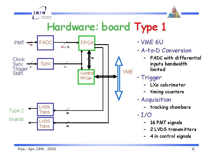
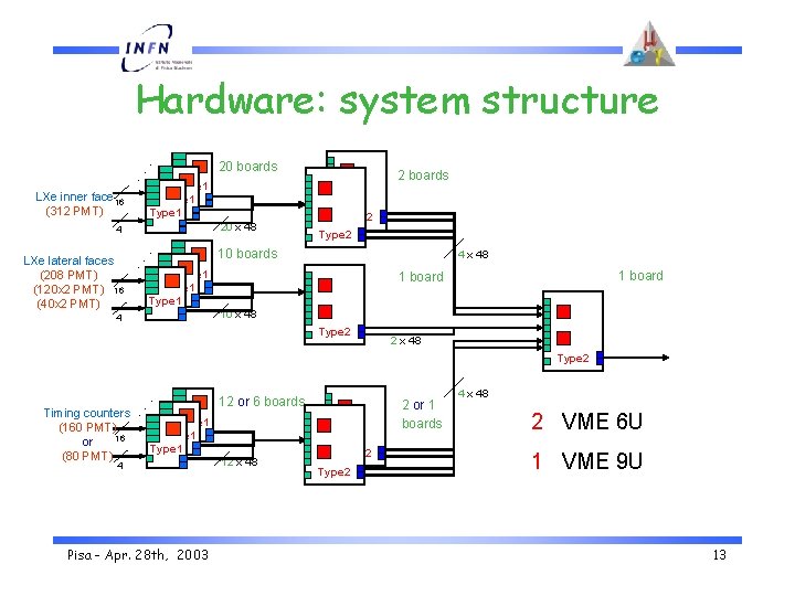
Hardware: board Type 1 PMT Clock Sync Trigger Start 16 FADC • VME 6 U • A-to-D Conversion FPGA 16 x 10 48 4 Sync 4 Control FPGA VME – FADC with differential inputs bandwidth limited • Trigger – LXe calorimeter – timing counters • Acquisition Type 2 boards – tracking chambers LVDS Trans 48 Pisa - Apr. 28 th, 2003 • I/O – 16 PMT signals – 2 LVDS transmitters – 4 in control signals 11

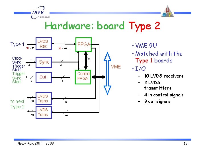
Hardware: board Type 2 Type 1 Clock Sync Trigger Start Trigger Sync Start to next Type 2 10 x 18 LVDS Rec Sync 4 3 Out 18 LVDS Trans Pisa - Apr. 28 th, 2003 FPGA 10 x 48 48 4 VME Control FPGA 3 48 • VME 9 U • Matched with the Type 1 boards • I/O – 10 LVDS receivers – 2 LVDS transmitters – 4 in control signals – 3 out signals 48 12

. . . Hardware: system structure LXe inner face 16 (312 PMT) Type 1 20 x 48 . . . 4 LXe lateral faces (208 PMT) (120 x 2 PMT) 16 (40 x 2 PMT) 20 boards 2 boards Type 2 10 boards 4 x 48 Type 1 1 board 10 x 48 4 Type 2 2 x 48 . Type 2 . . Timing counters (160 PMT) 16 or (80 PMT) 12 or 6 boards Type 1 4 Pisa - Apr. 28 th, 2003 12 x 48 2 or 1 boards Type 2 4 x 48 2 VME 6 U 1 VME 9 U 13

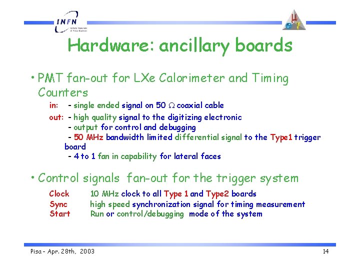
Hardware: ancillary boards • PMT fan-out for LXe Calorimeter and Timing Counters in: - single ended signal on 50 coaxial cable out: - high quality signal to the digitizing electronic - output for control and debugging - 50 MHz bandwidth limited differential signal to the Type 1 trigger board - 4 to 1 fan in capability for lateral faces • Control signals fan-out for the trigger system Clock Sync Start 10 MHz clock to all Type 1 and Type 2 boards high speed synchronization signal for timing measurement Run or control/debugging mode of the system Pisa - Apr. 28 th, 2003 14

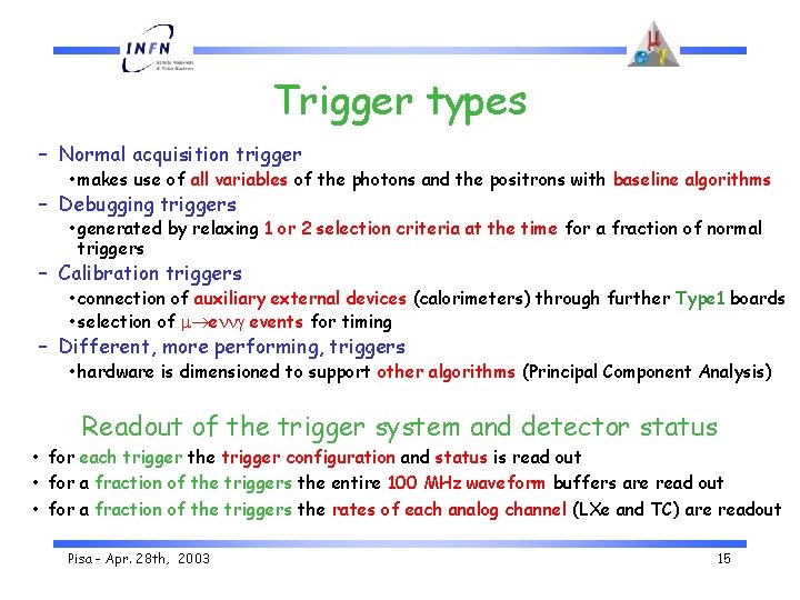
Trigger types – Normal acquisition trigger • makes use of all variables of the photons and the positrons with baseline algorithms – Debugging triggers • generated by relaxing 1 or 2 selection criteria at the time for a fraction of normal triggers – Calibration triggers • connection of auxiliary external devices (calorimeters) through further Type 1 boards • selection of e events for timing – Different, more performing, triggers • hardware is dimensioned to support other algorithms (Principal Component Analysis) Readout of the trigger system and detector status • for each trigger the trigger configuration and status is read out • for a fraction of the triggers the entire 100 MHz waveform buffers are read out • for a fraction of the triggers the rates of each analog channel (LXe and TC) are readout Pisa - Apr. 28 th, 2003 15

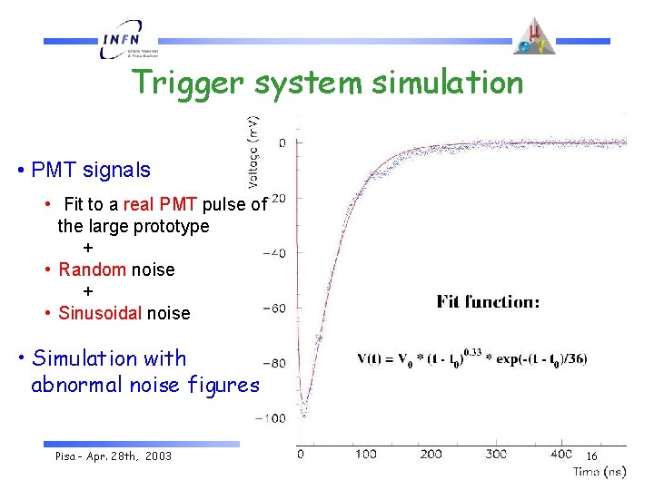
Trigger system simulation • PMT signals • Fit to a real PMT pulse of the large prototype + • Random noise + • Sinusoidal noise • Simulation with abnormal noise figures Pisa - Apr. 28 th, 2003 16

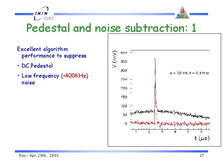
Pedestal and noise subtraction: 1 Excellent algorithm performance to suppress • DC Pedestal • Low frequency (<400 KHz) noise Pisa - Apr. 28 th, 2003 17

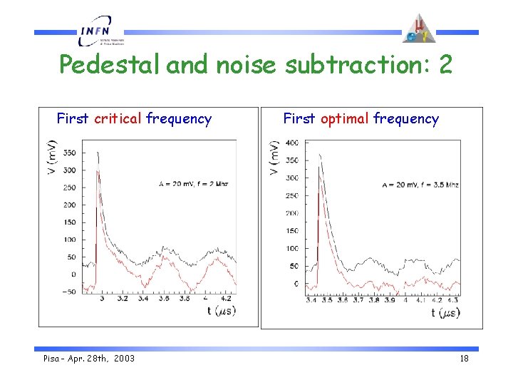
Pedestal and noise subtraction: 2 First critical frequency Pisa - Apr. 28 th, 2003 First optimal frequency 18

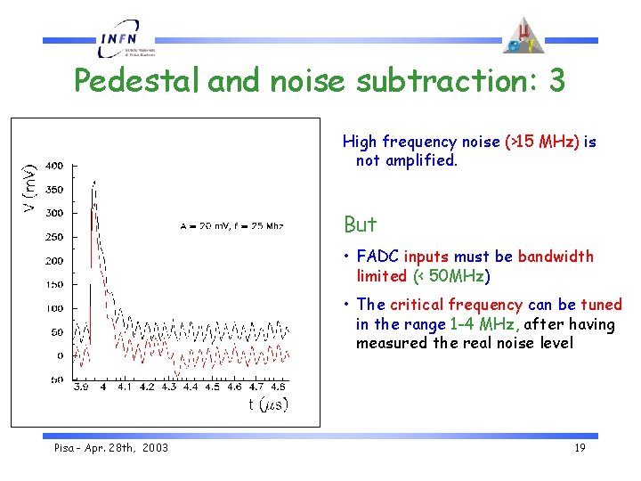
Pedestal and noise subtraction: 3 High frequency noise (>15 MHz) is not amplified. But • FADC inputs must be bandwidth limited (< 50 MHz) • The critical frequency can be tuned in the range 1 -4 MHz, after having measured the real noise level Pisa - Apr. 28 th, 2003 19

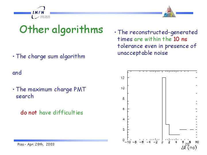
Other algorithms • The charge sum algorithm • The reconstructed-generated times are within the 10 ns tolerance even in presence of unacceptable noise and • The maximum charge PMT search do not have difficulties Pisa - Apr. 28 th, 2003 20

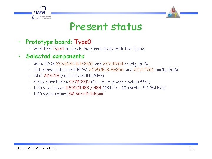
Present status • Prototype board: Type 0 – Modified Type 1 to check the connectivity with the Type 2 • Selected components – – – Main FPGA XCV 812 E-8 -FG 900 and XCV 18 V 04 config. ROM Interface and control FPGA XCV 50 E-8 -FG 256 and XCV 17 V 01 config. ROM ADC AD 9218 (dual 10 bits 100 MHz) Clock distribution CY 7 B 993 V (DLL multi-phase clock buffer) LVDS serializer DS 90 CR 483 / 484 (48 bits - 100 MHz - 5. 1 Gbits/s) LVDS connectors 3 M Mini-D-Ribbon Pisa - Apr. 28 th, 2003 21

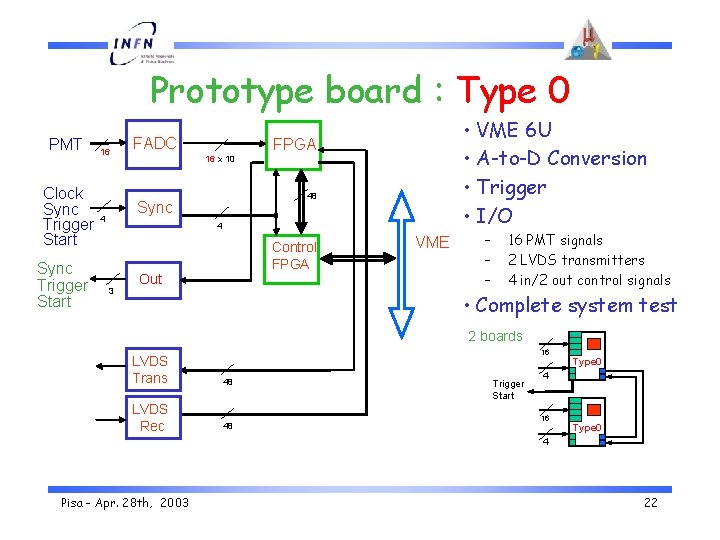
Prototype board : Type 0 PMT Clock Sync Trigger Start 16 FADC 16 x 10 48 Sync 4 • VME 6 U • A-to-D Conversion • Trigger • I/O FPGA 4 3 Control FPGA Out VME – – – 16 PMT signals 2 LVDS transmitters 4 in/2 out control signals • Complete system test 2 boards 16 LVDS Trans 48 LVDS Rec 48 Trigger Start Type 0 4 16 Type 0 4 Pisa - Apr. 28 th, 2003 22

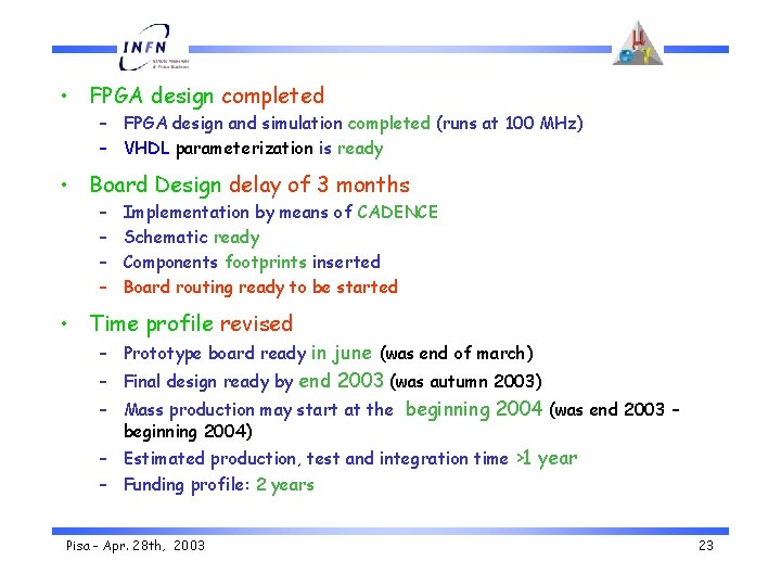
• FPGA design completed – FPGA design and simulation completed (runs at 100 MHz) – VHDL parameterization is ready • Board Design delay of 3 months – – Implementation by means of CADENCE Schematic ready Components footprints inserted Board routing ready to be started • Time profile revised – Prototype board ready in june (was end of march) – Final design ready by end 2003 (was autumn 2003) – Mass production may start at the beginning 2004 (was end 2003 – beginning 2004) – Estimated production, test and integration time >1 year – Funding profile: 2 years Pisa - Apr. 28 th, 2003 23

Detailed functional description Pisa - Apr. 28 th, 2003 24

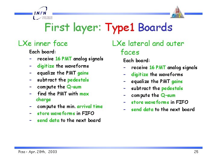
First layer: Type 1 Boards LXe inner face Each board: – receive 16 PMT analog signals – digitize the waveforms – equalize the PMT gains – subtract the pedestals – compute the Q-sum – find the PMT with max charge – compute the min. arrival time – store waveforms in FIFO – send data to the next board Pisa - Apr. 28 th, 2003 LXe lateral and outer faces Each board: – receive 16 PMT analog signals – digitize the waveforms – equalize the PMT gains – subtract the pedestals – compute the Q-sum – store waveforms in FIFO – send data to the next board 25

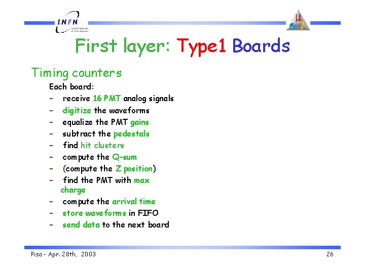
First layer: Type 1 Boards Timing counters Each board: – receive 16 PMT analog signals – digitize the waveforms – equalize the PMT gains – subtract the pedestals – find hit clusters – compute the Q-sum – (compute the Z position) – find the PMT with max charge – compute the arrival time – store waveforms in FIFO – send data to the next board Pisa - Apr. 28 th, 2003 26

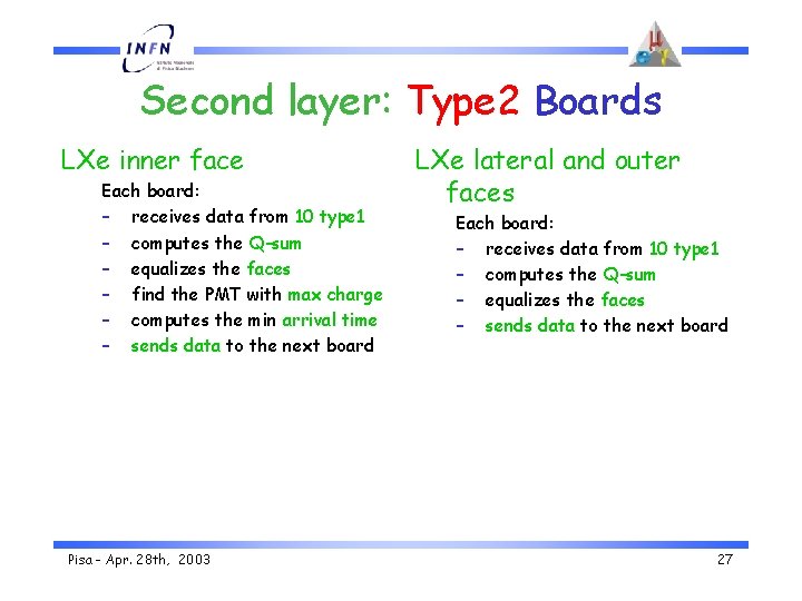
Second layer: Type 2 Boards LXe inner face Each board: – receives data from 10 type 1 – computes the Q-sum – equalizes the faces – find the PMT with max charge – computes the min arrival time – sends data to the next board Pisa - Apr. 28 th, 2003 LXe lateral and outer faces Each board: – receives data from 10 type 1 – computes the Q-sum – equalizes the faces – sends data to the next board 27

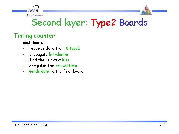
Second layer: Type 2 Boards Timing counter Each board: – receives data from 6 type 1 – propagate hit-cluster – find the relevant hits – computes the arrival time – sends data to the final board Pisa - Apr. 28 th, 2003 28

Final layer : Type 2 Board The board – – – receives data from type-2 boards computes E , Q and F computes the arrival time computes Q and F for the positron computes the Positron arrival time generates triggers – Normal acquisition trigger • makes use of all variables of the photons and the positrons with baseline algorithms – Debugging triggers • generated by relaxing 1 or 2 selection criteria at the time for a fraction of normal triggers – Calibration triggers • connection of auxiliary external devices (calorimeters) through further Type 1 boards • selection of e events for timing Pisa - Apr. 28 th, 2003 29

– Different, more performing, triggers • hardware is dimensioned to support other algorithms (Principal Component Analysis) Readout of the trigger system and detector status • for each trigger the trigger configuration and status is read out • for a fraction of the triggers the entire 100 MHz waveform buffers are read out • for a fraction of the triggers the rates of each analog channel (LXe and TC) are read out Pisa - Apr. 28 th, 2003 30

Details of the Trigger System • Flexibility – – the present trigger algorithms could not be the final ones LXe and Timing Counters have different algorithms – – – limited data flow through the bus standard commercially exploitable front panel space and reduced number of stages – – compromise between accuracy & cost many other electronic components can run at 100 MHz – 10 bit FADC are available and adequate • Standard (VME 6 U and 9 U) • FADC Frequency (100 MHz) • Dynamic Range – Pisa - Apr. 28 th, 2003 31

• Board synchronization – – events are uniformly distributed in time the event time is a basic trigger variable synchronous operation of the trigger system • external clock distribution and PLL components • synchronization signal after each L 2 trigger • Interconnections – – LVDS up to 5 Gbits/s on 9 differential couples are available • reduced front panel space • reduced amount of cables large latency : tran. (1. 5*T+4. 9) rec. (3. 5*T+4. 4) cable (10) = Tot (7*T) • Minimal different types of boards (2 Types) – Type 1 : analog to digital conversion – – Type 2 : pure digital arranged in a tree structure • Possible other uses – acquisition board for the tracking chambers Pisa - Apr. 28 th, 2003 32

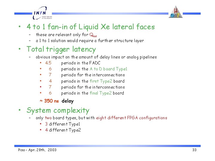
• 4 to 1 fan-in of Liquid Xe lateral faces – – these are relevant only for Qtot a 1 to 1 solution would require a further structure layer • Total trigger latency – obvious impact on the amount of delay lines or analog pipelines • 4. 5 periods in the FADC • 6 periods in the A to D board Type 1 • 7 periods for the interconnections • 4 periods in the first Type 2 board • 7 periods for the interconnections • 6 periods in the final Type 2 board ~ 350 ns delay • System complexity – only two board types, but with eight different FPGA configurations • 3 different Type 1 • 4 different Type 2 Pisa - Apr. 28 th, 2003 33