Unit 1 JFET Contents Introduction to JFET Types
- Slides: 61

Unit 1: JFET

Contents • Introduction to JFET, Types, Construction, Operation. • Static Characteristics, Pinch off voltage. • FET Volt-Ampere characteristics. • FET Configurations (CS/CD/CG) and their Comparison. • Biasing of FET (Self). FET as an amplifier and its analysis (CS) and its frequency response. • Small signal model, FET as High Impedance circuits.

JFET (Junction Field Effect Transistor) • Unipolar device (one polarity of charge carrier) • Voltage controlled (gate voltage controls drain current) • High input impedance ( 109 -1012 ) • No minority carrier storage • Source and drain are interchangeable in most low-frequency applications

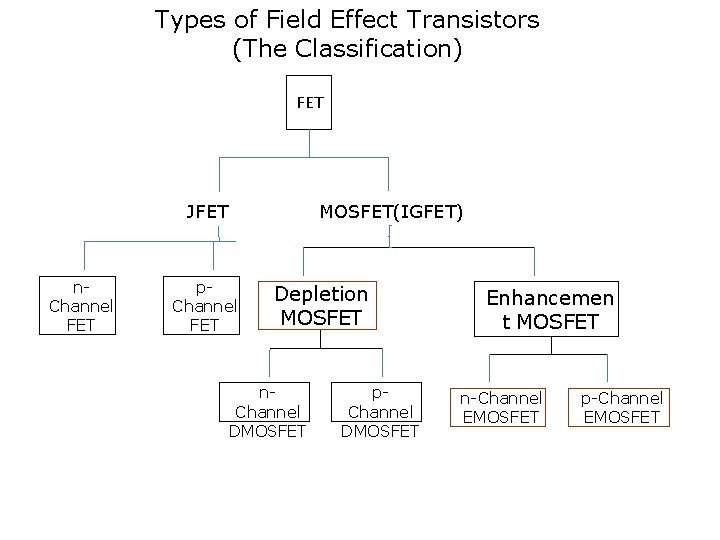
Types of Field Effect Transistors (The Classification) FET JFET n. Channel FET MOSFET(IGFET) p. Channel FET Depletion MOSFET n. Channel DMOSFET p. Channel DMOSFET Enhancemen t MOSFET n-Channel EMOSFET p-Channel EMOSFET

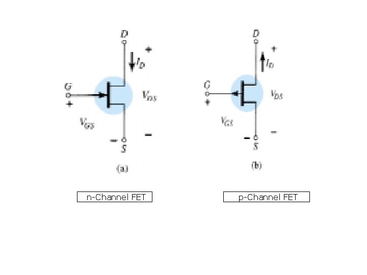
n-Channel FET p-Channel FET

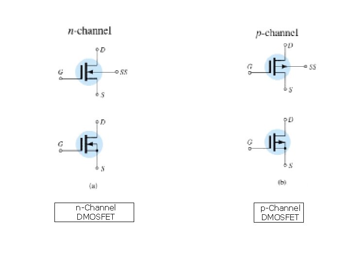
n-Channel DMOSFET p-Channel DMOSFET

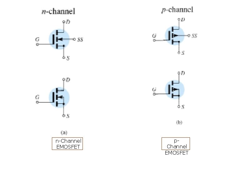
n-Channel EMOSFET p. Channel EMOSFET

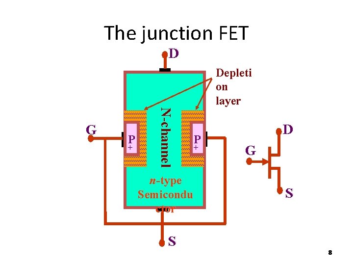
The junction FET D Depleti on layer P + N-channel G P + n-type Semicondu ctor S D G S 8

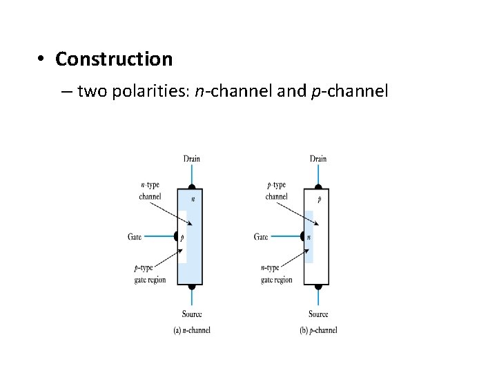
• Construction – two polarities: n-channel and p-channel

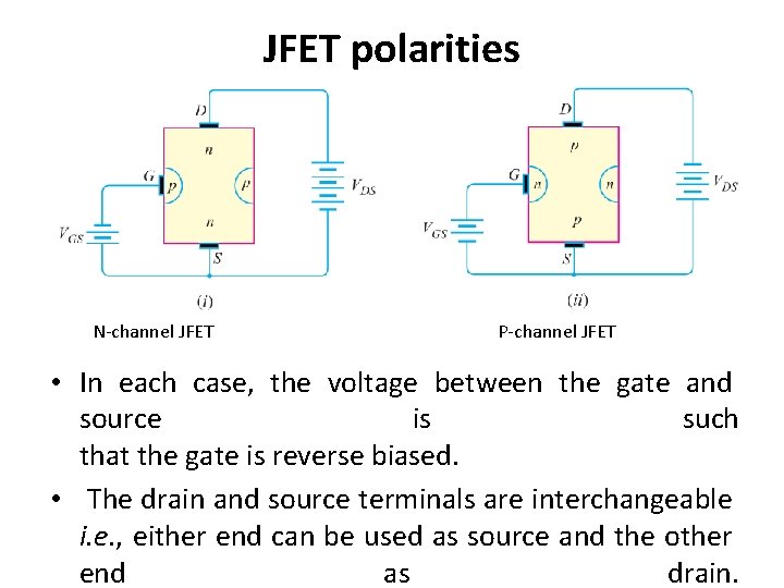
JFET polarities N-channel JFET P-channel JFET • In each case, the voltage between the gate and source is such that the gate is reverse biased. • The drain and source terminals are interchangeable i. e. , either end can be used as source and the other end as drain.

Points to be Noted • The input circuit (i. e. gate to source) of a JFET is reverse biased. This means that the device has high input impedance. • The drain is so biased w. r. t. source that drain current ID flows from the source to drain. • In all JFETs, source current IS is equal to the drain current i. e. IS = ID

Principle • JFET operates on the principle that width and hence resistance of the conducting channel can be varied by changing the reverse voltage VGS. • In other words, the magnitude of drain current (ID) can be changed by altering VGS

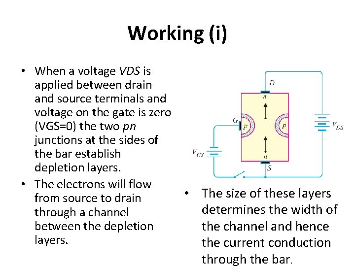
Working (i) • When a voltage VDS is applied between drain and source terminals and voltage on the gate is zero (VGS=0) the two pn junctions at the sides of the bar establish depletion layers. • The electrons will flow • The size of these layers from source to drain determines the width of through a channel between the depletion the channel and hence layers. the current conduction through the bar.

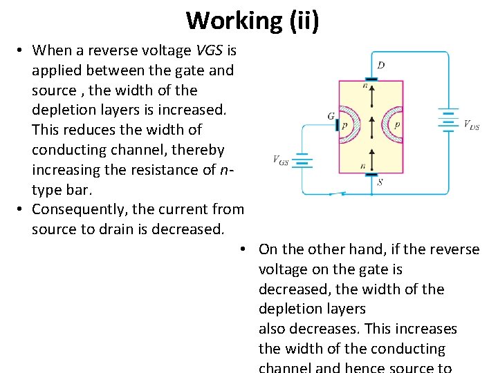
Working (ii) • When a reverse voltage VGS is applied between the gate and source , the width of the depletion layers is increased. This reduces the width of conducting channel, thereby increasing the resistance of ntype bar. • Consequently, the current from source to drain is decreased. • On the other hand, if the reverse voltage on the gate is decreased, the width of the depletion layers also decreases. This increases the width of the conducting

Notes • Current from source to drain can be controlled by the application of potential (i. e. electric field) on the gate. For this reason, the device is called field effect transistor. A • p-channel JFET operates in the same manner as an n -channel JFET except that channel current carriers will be the holes instead of electrons and the polarities of VGS and V DS are reversed.

• If the reverse voltage VGS on the gate is continuously increased, a state is reached when the two depletion layers touch each other and the channel is cut off. Under such conditions, the channel becomes a nonconductor.

Output Characteristics of JFET • The curve between drain current (ID) and drain-source voltage (VDS ) of a JFET at constant gate source voltage (VGS) is known as output characteristics of JFET.

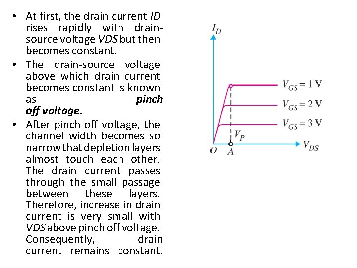
• At first, the drain current ID rises rapidly with drainsource voltage VDS but then becomes constant. • The drain-source voltage above which drain current becomes constant is known as pinch off voltage. • After pinch off voltage, the channel width becomes so narrow that depletion layers almost touch each other. The drain current passes through the small passage between these layers. Therefore, increase in drain current is very small with VDS above pinch off voltage. Consequently, drain current remains constant.

It is the drain current with source short-circuited to gate (i. e. VGS = 0) and drain voltage (VDS) equal to pinch off voltage. It is sometimes called zero-bias current.

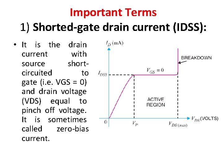
Important Terms 1) Shorted-gate drain current (IDSS): • It is the drain current with source shortcircuited to gate (i. e. VGS = 0) and drain voltage (VDS) equal to pinch off voltage. It is sometimes called zero-bias current.

• Since IDSS is measured under shorted gate conditions, it is the maximum drain current that you can get with normal operation of JFET. • There is a maximum drain voltage [VDS (max)] that can be applied to a JFET. If the drain voltage exceeds VDS (max), JFET would breakdown. • The region between VP and VDS (max) (breakdown voltage) is called constant-current region or active region. • As long as VDS is kept within this range, ID will remain constant for a constant value of VGS. • In other words, in the active region, JFET behaves as a constant–current device. For proper working of JFET, it must be operated in the active region.

2) Pinch off Voltage (VP): It is the minimum drain-source voltage at which the drain current essentially becomes constant. 3) Gate-source cut off voltage VGS (off) : It is the gate-source voltage where the channel is completely cut off and the drain current becomes zero.

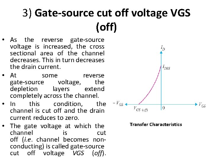
3) Gate-source cut off voltage VGS (off) • As the reverse gate-source voltage is increased, the cross sectional area of the channel decreases. This in turn decreases the drain current. • At some reverse gate-source voltage, the depletion layers extend completely across the channel. • In this condition, the channel is cut off and the drain current reduces to zero. • The gate voltage at which the channel is cut off (i. e. channel becomes nonconducting) is called gate-source cut off voltage VGS (off). Transfer Characteristics

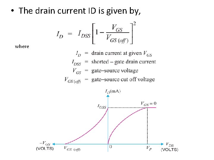
Expression for Drain Current (ID) • We know that gate-source cut off voltage [i. e. VGS (off)] on the transfer characteristic is equal to pinch off voltage VP on the drain characteristic i. e. VP = |VGS (off)| For example, If a JFET has VGS (off) = − 4 V, then VP = 4 V

• The drain current ID is given by, where

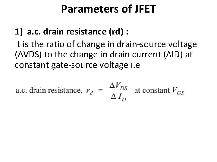
Parameters of JFET 1) a. c. drain resistance (rd) : It is the ratio of change in drain-source voltage (ΔVDS) to the change in drain current (ΔID) at constant gate-source voltage i. e

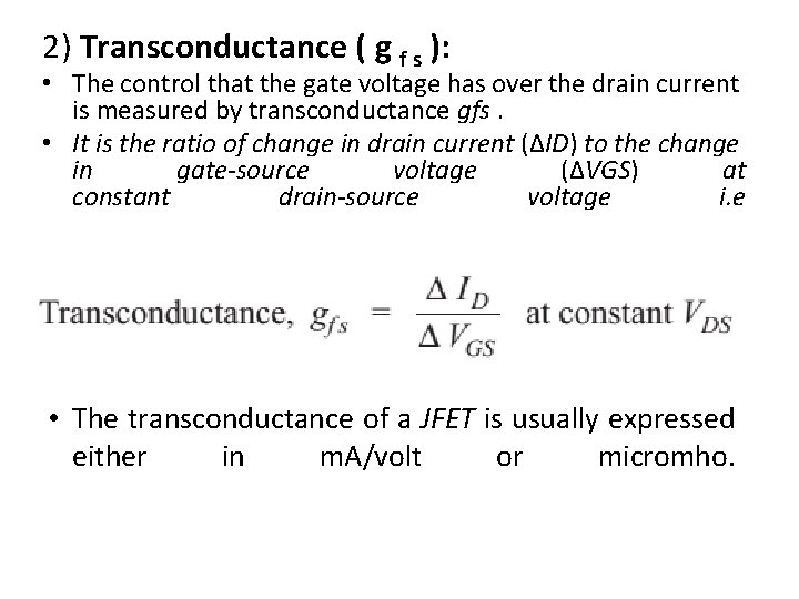
2) Transconductance ( g f s ): • The control that the gate voltage has over the drain current is measured by transconductance gfs. • It is the ratio of change in drain current (ΔID) to the change in gate-source voltage (ΔVGS) at constant drain-source voltage i. e • The transconductance of a JFET is usually expressed either in m. A/volt or micromho.

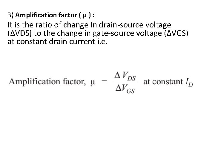
3) Amplification factor ( µ ) : It is the ratio of change in drain-source voltage (ΔVDS) to the change in gate-source voltage (ΔVGS) at constant drain current i. e.

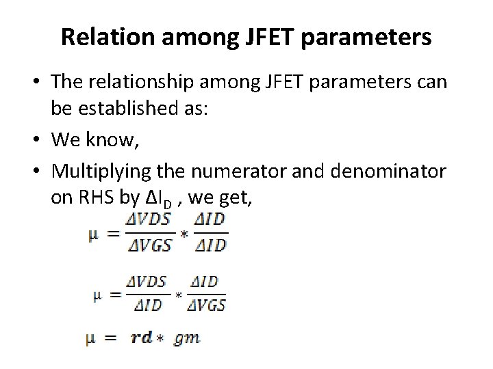
Relation among JFET parameters • The relationship among JFET parameters can be established as: • We know, • Multiplying the numerator and denominator on RHS by ΔID , we get,

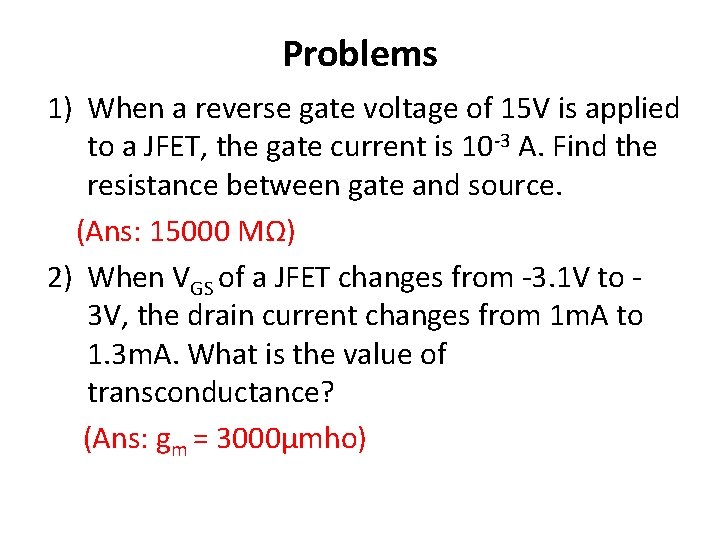
Problems 1) When a reverse gate voltage of 15 V is applied to a JFET, the gate current is 10 -3 A. Find the resistance between gate and source. (Ans: 15000 MΩ) 2) When VGS of a JFET changes from -3. 1 V to 3 V, the drain current changes from 1 m. A to 1. 3 m. A. What is the value of transconductance? (Ans: gm = 3000µmho)

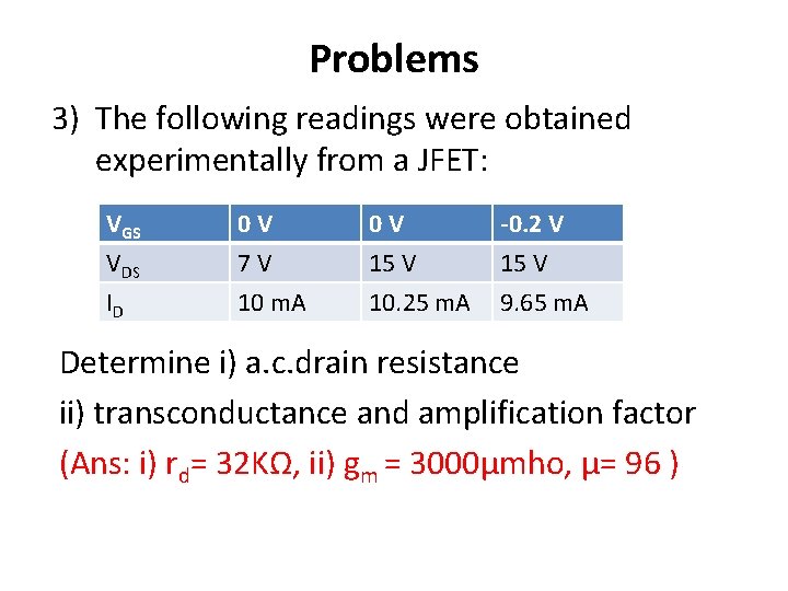
Problems 3) The following readings were obtained experimentally from a JFET: VGS VDS ID 0 V 7 V 10 m. A 0 V 15 V 10. 25 m. A -0. 2 V 15 V 9. 65 m. A Determine i) a. c. drain resistance ii) transconductance and amplification factor (Ans: i) rd= 32 KΩ, ii) gm = 3000µmho, µ= 96 )

JFET Biasing • For the properation of n-channel JFET, gate must be negative w. r. t. source. • This can be achieved either by inserting a battery in the gate circuit or by a circuit known as biasing circuit. • The latter method is preferred because batteries are costly and require frequent replacement.

1. Bias battery : In this method, JFET is biased by a bias battery VGG. This battery ensures that gate is always negative w. r. t. source during all parts of the signal. 2. Biasing circuit : The biasing circuit uses supply voltage VDD to provide the necessary bias. Two most commonly used methods are (i) selfbias (ii) potential divider method.

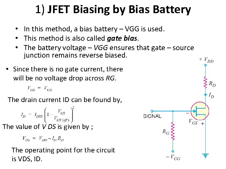
1) JFET Biasing by Bias Battery • In this method, a bias battery – VGG is used. • This method is also called gate bias. • The battery voltage – VGG ensures that gate – source junction remains reverse biased. • Since there is no gate current, there will be no voltage drop across RG. The drain current ID can be found by, The value of V DS is given by ; The operating point for the circuit is VDS, ID.

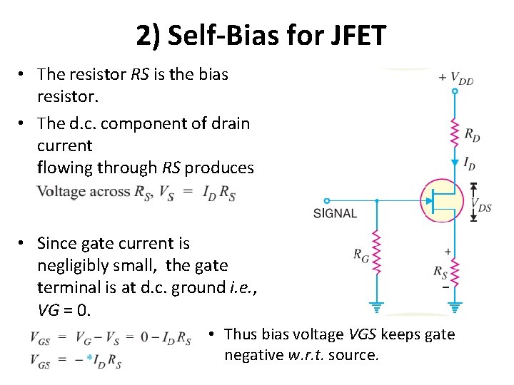
2) Self-Bias for JFET • The resistor RS is the bias resistor. • The d. c. component of drain current flowing through RS produces the desired bias voltage. • Since gate current is negligibly small, the gate terminal is at d. c. ground i. e. , VG = 0. • Thus bias voltage VGS keeps gate negative w. r. t. source.

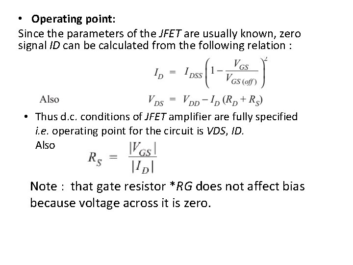
• Operating point: Since the parameters of the JFET are usually known, zero signal ID can be calculated from the following relation : • Thus d. c. conditions of JFET amplifier are fully specified i. e. operating point for the circuit is VDS, ID. Also Note : that gate resistor *RG does not affect bias because voltage across it is zero.

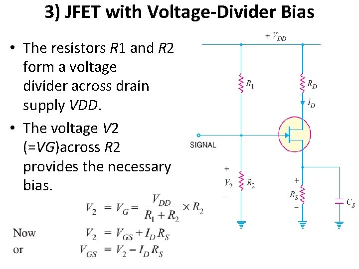
3) JFET with Voltage-Divider Bias • The resistors R 1 and R 2 form a voltage divider across drain supply VDD. • The voltage V 2 (=VG)across R 2 provides the necessary bias. •

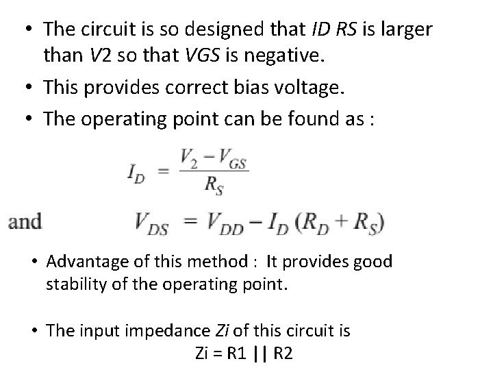
• The circuit is so designed that ID RS is larger than V 2 so that VGS is negative. • This provides correct bias voltage. • The operating point can be found as : • Advantage of this method : It provides good stability of the operating point. • The input impedance Zi of this circuit is Zi = R 1 || R 2

JFET Connections • A JFET can be connected in a circuit in the following three ways : (i) Common source connection (ii) Common gate connection (iii) Common drain connection • The common source connection is the most widely used arrangement. It is because this connection provides high input impedance, good voltage gain and a moderate output impedance. However, the circuit produces a phase reversal i. e. , output signal is 180° out of phase with the input signal.

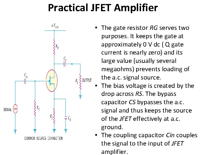
Practical JFET Amplifier • The gate resistor RG serves two purposes. It keeps the gate at approximately 0 V dc ( Q gate current is nearly zero) and its large value (usually several megaohms) prevents loading of the a. c. signal source. • The bias voltage is created by the drop across RS. The bypass capacitor CS bypasses the a. c. signal and thus keeps the source of the JFET effectively at a. c. ground. • The coupling capacitor Cin couples the signal to the input of JFET amplifier.

D. C. and A. C. Equivalent Circuits of JFET • Both d. c. and a. c. conditions prevail in a JFET amplifier. • The d. c. sources set up d. c. currents and voltages whereas the a. c. source (i. e. signal) produces fluctuations in the JFET currents and voltages. • Therefore, a simple way to analyze the action of a JFET amplifier is to split the circuit into two parts viz. d. c. equivalent circuit and a. c. equivalent circuit. • The d. c. equivalent circuit will determine the operating point (d. c. bias levels) for the circuit • a. c. equivalent circuit determines the output voltage and hence voltage gain of the circuit.

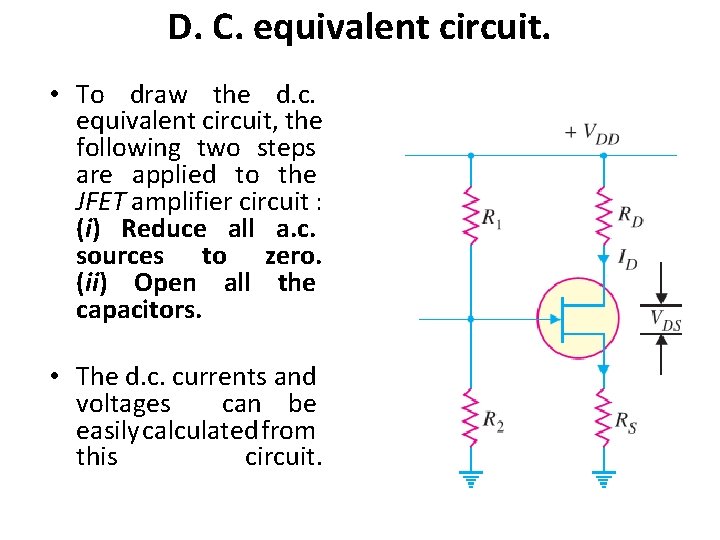
D. C. equivalent circuit. • To draw the d. c. equivalent circuit, the following two steps are applied to the JFET amplifier circuit : (i) Reduce all a. c. sources to zero. (ii) Open all the capacitors. • The d. c. currents and voltages can be easily calculated from this circuit.

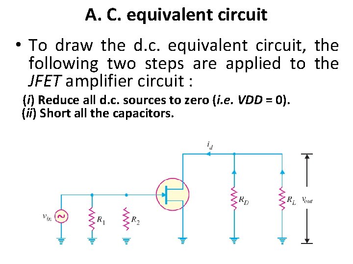
A. C. equivalent circuit • To draw the d. c. equivalent circuit, the following two steps are applied to the JFET amplifier circuit : (i) Reduce all d. c. sources to zero (i. e. VDD = 0). (ii) Short all the capacitors.

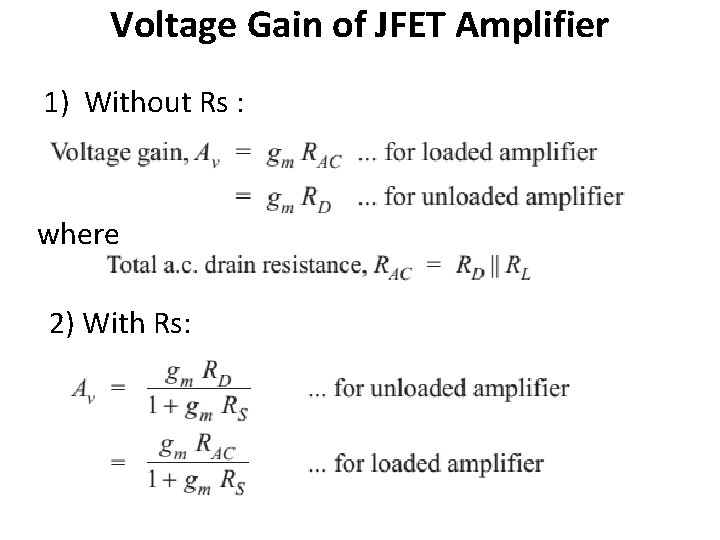
Voltage Gain of JFET Amplifier 1) Without Rs : where 2) With Rs:

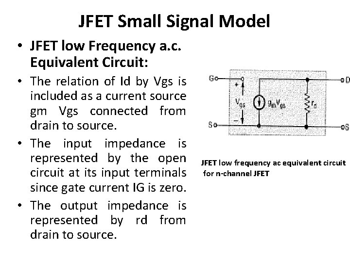
JFET Small Signal Model • JFET low Frequency a. c. Equivalent Circuit: • The relation of Id by Vgs is included as a current source gm Vgs connected from drain to source. • The input impedance is represented by the open circuit at its input terminals since gate current IG is zero. • The output impedance is represented by rd from drain to source. JFET low frequency ac equivalent circuit for n-channel JFET

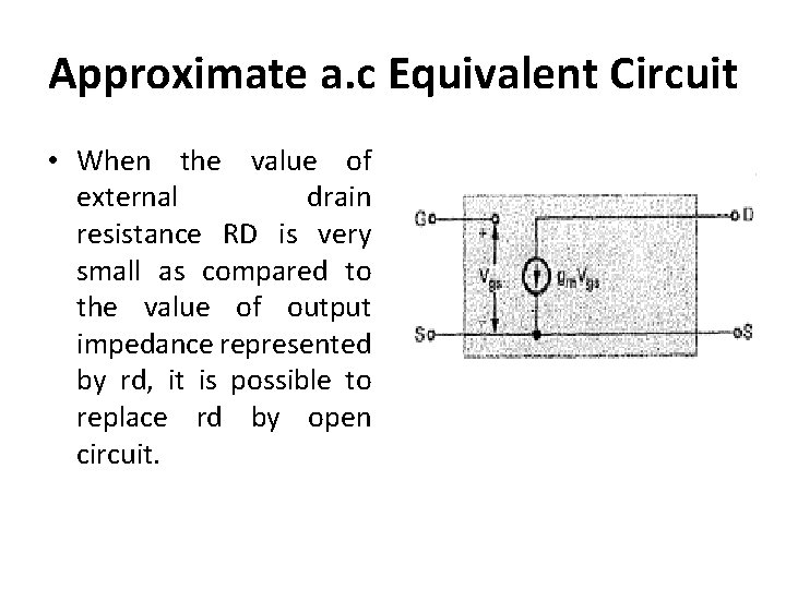
Approximate a. c Equivalent Circuit • When the value of external drain resistance RD is very small as compared to the value of output impedance represented by rd, it is possible to replace rd by open circuit.

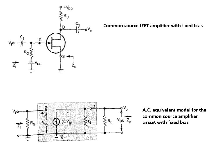
Common source JFET amplifier with fixed bias A. C. equivalent model for the common source amplifier circuit with fixed bias

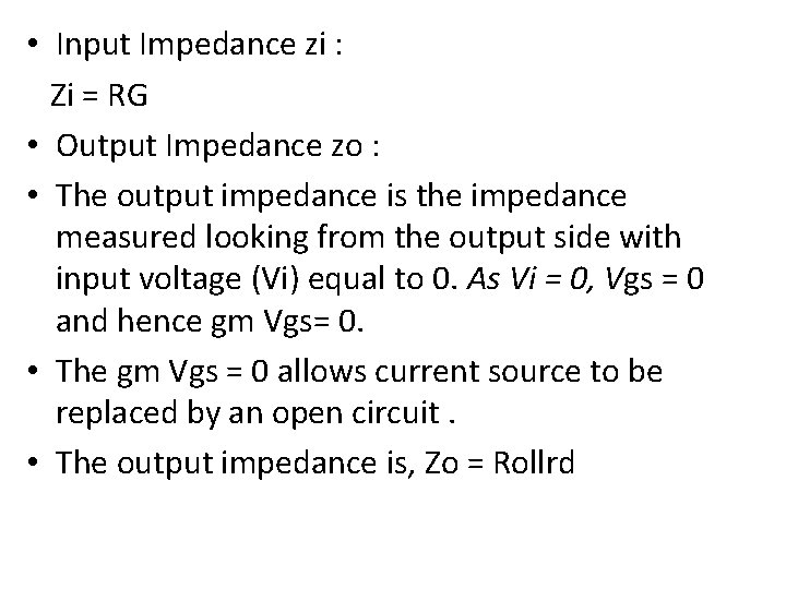
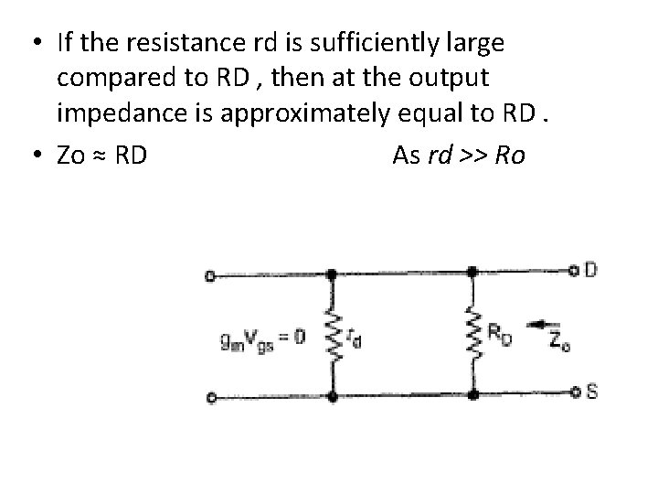
• Input Impedance zi : Zi = RG • Output Impedance zo : • The output impedance is the impedance measured looking from the output side with input voltage (Vi) equal to 0. As Vi = 0, Vgs = 0 and hence gm Vgs= 0. • The gm Vgs = 0 allows current source to be replaced by an open circuit. • The output impedance is, Zo = Rollrd

• If the resistance rd is sufficiently large compared to RD , then at the output impedance is approximately equal to RD. • Zo ≈ RD As rd >> Ro

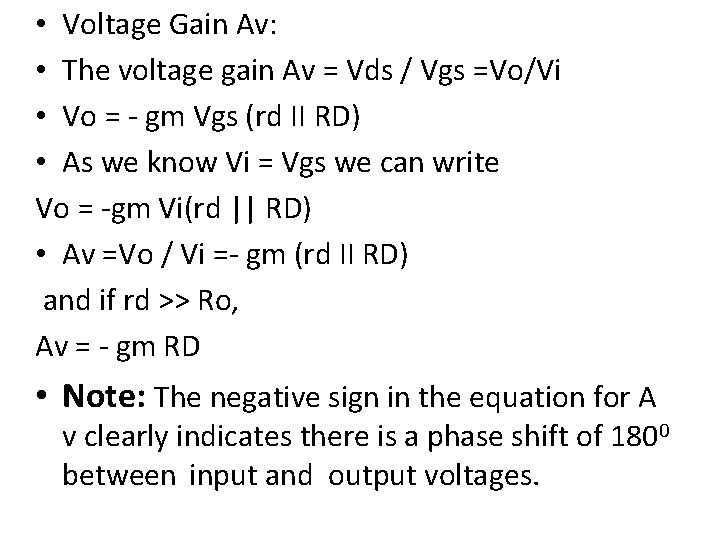
• Voltage Gain Av: • The voltage gain Av = Vds / Vgs =Vo/Vi • Vo = - gm Vgs (rd II RD) • As we know Vi = Vgs we can write Vo = -gm Vi(rd || RD) • Av =Vo / Vi =- gm (rd II RD) and if rd >> Ro, Av = - gm RD • Note: The negative sign in the equation for A v clearly indicates there is a phase shift of 1800 between input and output voltages.

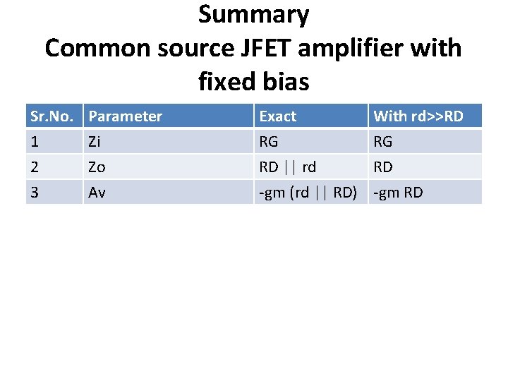
Summary Common source JFET amplifier with fixed bias Sr. No. 1 2 3 Parameter Zi Zo Av Exact RG RD || rd -gm (rd || RD) With rd>>RD RG RD -gm RD

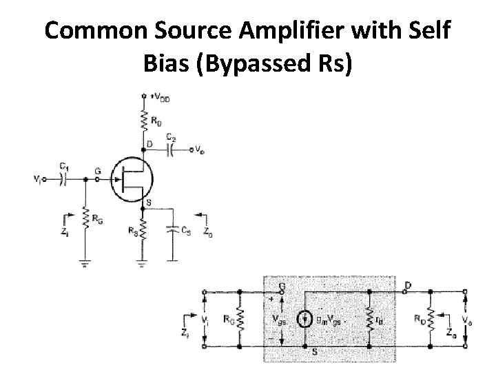
Common Source Amplifier with Self Bias (Bypassed Rs)

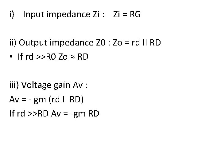
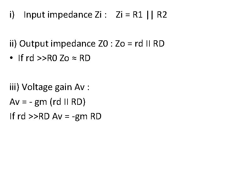
i) Input impedance Zi : Zi = RG ii) Output impedance Z 0 : Zo = rd II RD • If rd >>R 0 Zo ≈ RD iii) Voltage gain Av : Av = - gm (rd II RD) If rd >>RD Av = -gm RD

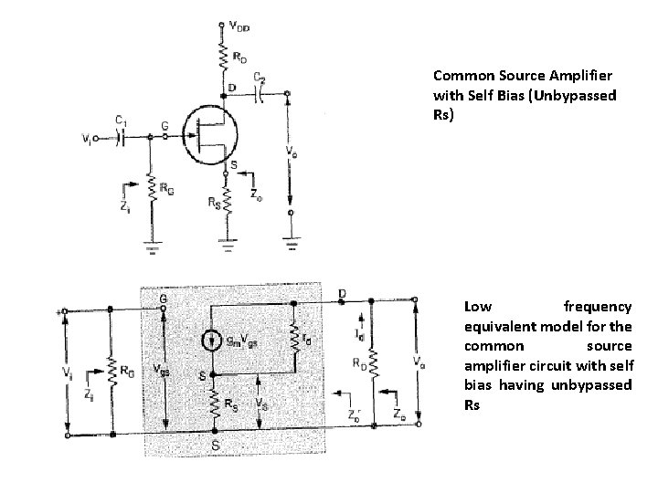
Common Source Amplifier with Self Bias (Unbypassed Rs) Low frequency equivalent model for the common source amplifier circuit with self bias having unbypassed Rs

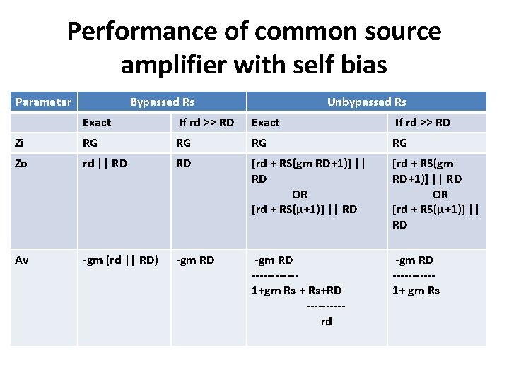
Performance of common source amplifier with self bias Parameter Bypassed Rs Unbypassed Rs Exact If rd >> RD Zi RG RG Zo rd || RD RD [rd + RS(gm RD+1)] || RD OR [rd + RS(µ+1)] || RD Av -gm (rd || RD) -gm RD ------1+gm Rs + Rs+RD -----rd -gm RD -----1+ gm Rs

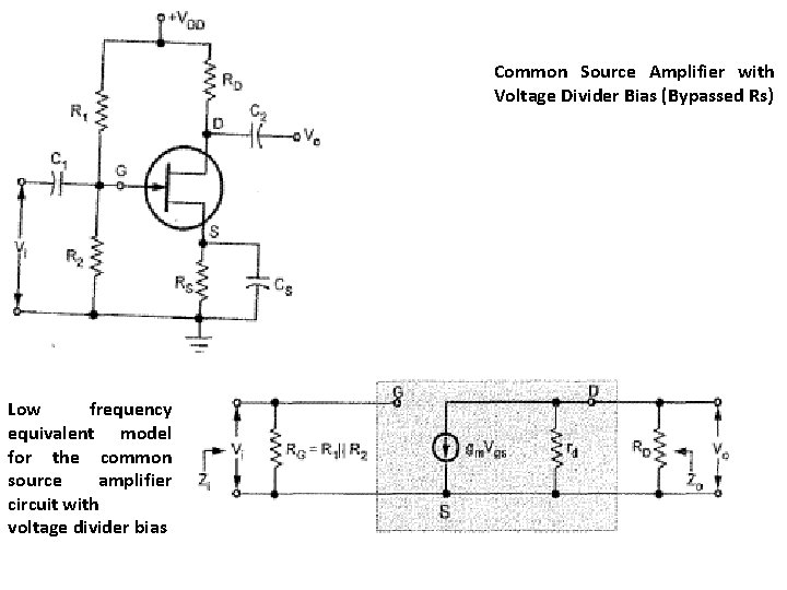
Common Source Amplifier with Voltage Divider Bias (Bypassed Rs) Low frequency equivalent model for the common source amplifier circuit with voltage divider bias

i) Input impedance Zi : Zi = R 1 || R 2 ii) Output impedance Z 0 : Zo = rd II RD • If rd >>R 0 Zo ≈ RD iii) Voltage gain Av : Av = - gm (rd II RD) If rd >>RD Av = -gm RD

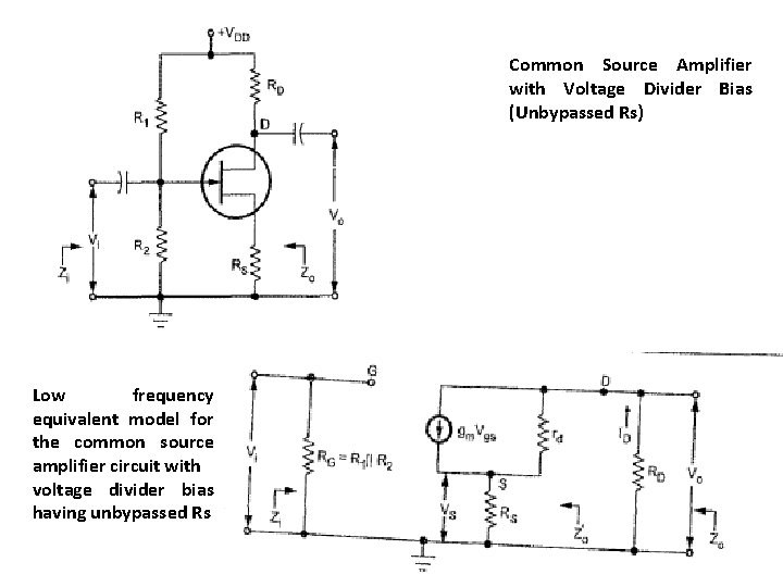
Common Source Amplifier with Voltage Divider Bias (Unbypassed Rs) Low frequency equivalent model for the common source amplifier circuit with voltage divider bias having unbypassed Rs

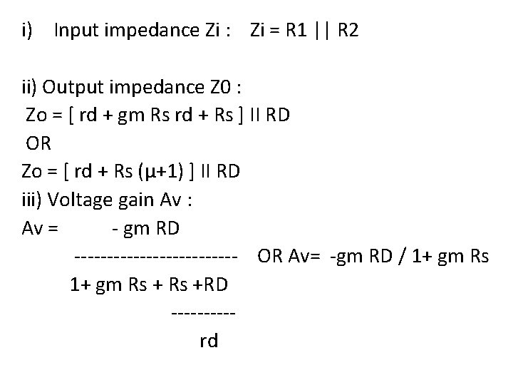
i) Input impedance Zi : Zi = R 1 || R 2 ii) Output impedance Z 0 : Zo = [ rd + gm Rs rd + Rs ] II RD OR Zo = [ rd + Rs (µ+1) ] II RD iii) Voltage gain Av : Av = - gm RD ------------- OR Av= -gm RD / 1+ gm Rs +RD -----rd

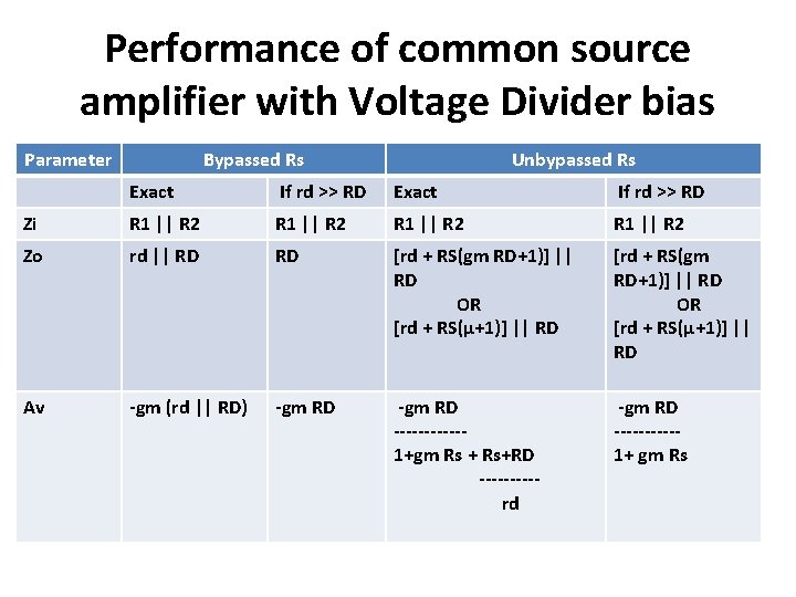
Performance of common source amplifier with Voltage Divider bias Parameter Bypassed Rs Unbypassed Rs Exact If rd >> RD Zi R 1 || R 2 Zo rd || RD RD [rd + RS(gm RD+1)] || RD OR [rd + RS(µ+1)] || RD Av -gm (rd || RD) -gm RD ------1+gm Rs + Rs+RD -----rd -gm RD -----1+ gm Rs

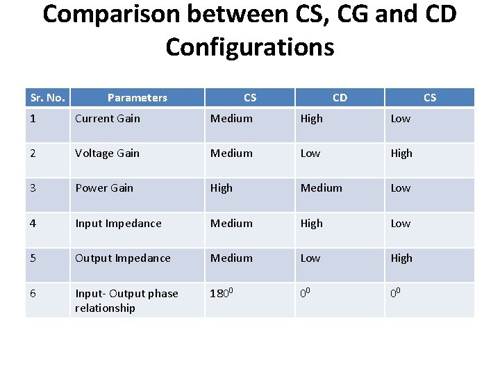
Comparison between CS, CG and CD Configurations Sr. No. Parameters CS CD CS 1 Current Gain Medium High Low 2 Voltage Gain Medium Low High 3 Power Gain High Medium Low 4 Input Impedance Medium High Low 5 Output Impedance Medium Low High 6 Input- Output phase relationship 1800 00 00