Flash Memory and a tour through FETs Conceptual






- Slides: 23

Flash Memory …and a tour through FETs

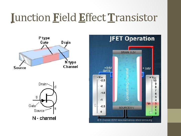
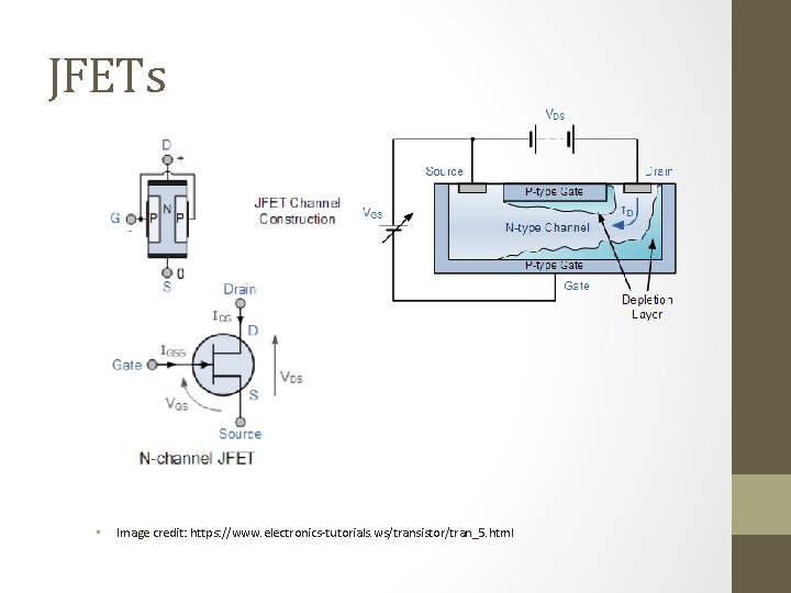
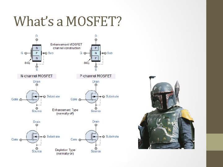
Conceptual Roadmap PN junction Connect a drain (D), Source (S), Gate(G) JFET Insert thin oxide layer between gate contact and doped substrate MOSFET Add a floating gate Flash Cell Put a bunch together in NAND or NOR configuration Flash Blocks Out pops an SD card or MCU flash memory! Modern Devices

Junction Field Effect Transistor

JFETs • Image credit: https: //www. electronics-tutorials. ws/transistor/tran_5. html

What’s a MOSFET?

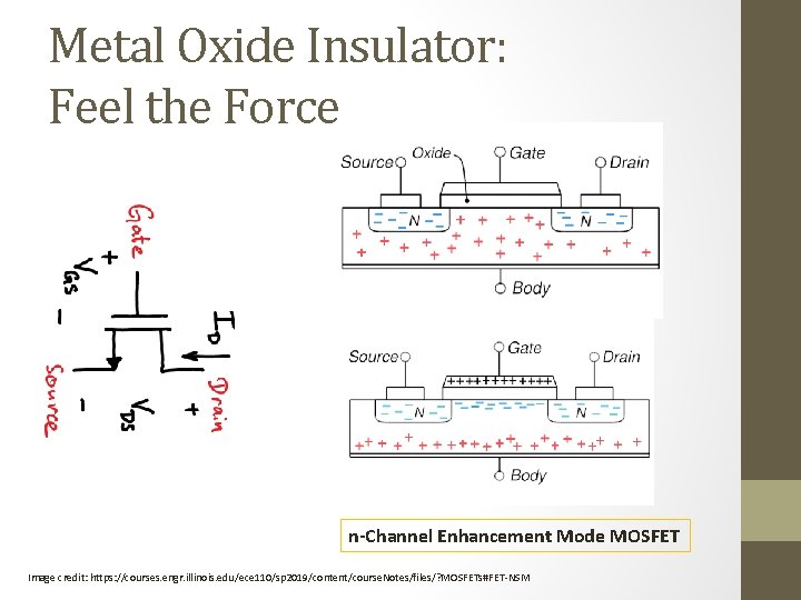
Metal Oxide Insulator: Feel the Force n-Channel Enhancement Mode MOSFET Image credit: https: //courses. engr. illinois. edu/ece 110/sp 2019/content/course. Notes/files/? MOSFETs#FET-NSM

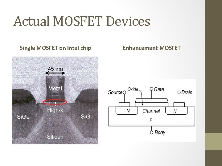
Actual MOSFET Devices Single MOSFET on Intel chip Enhancement MOSFET

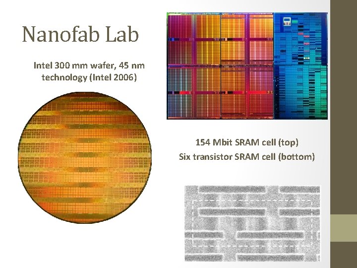
Nanofab Lab Intel 300 mm wafer, 45 nm technology (Intel 2006) 154 Mbit SRAM cell (top) Six transistor SRAM cell (bottom)

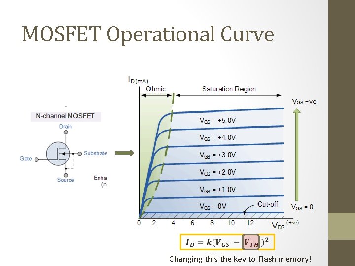
MOSFET Operational Curve Changing this the key to Flash memory!

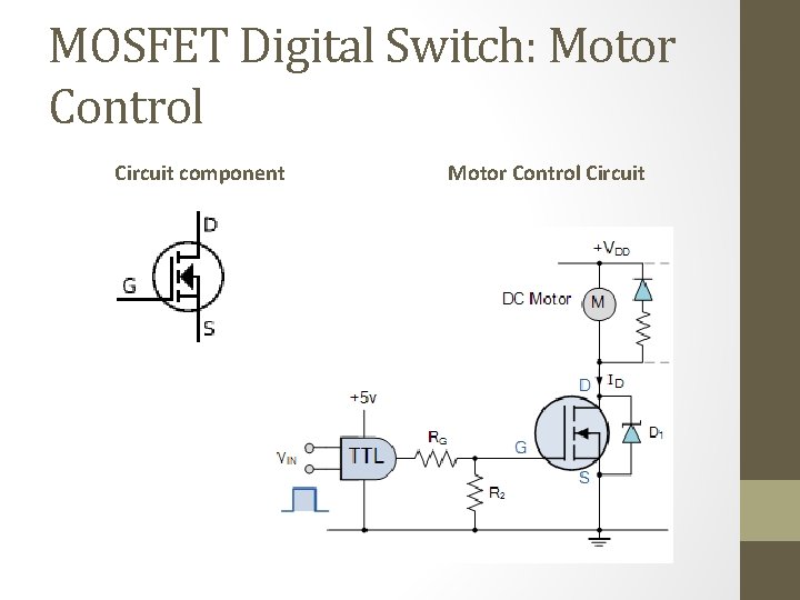
MOSFET Digital Switch: Motor Control Circuit component Motor Control Circuit

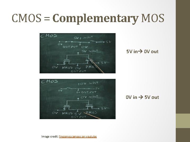
CMOS = Complementary MOS 5 V in 0 V out 0 V in 5 V out Image credit: fmgomezcampos on youtube

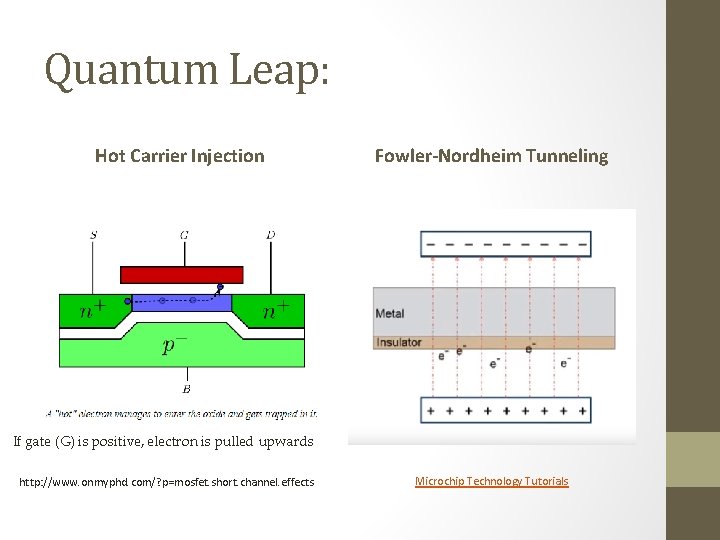
Quantum Leap: Hot Carrier Injection Fowler-Nordheim Tunneling If gate (G) is positive, electron is pulled upwards http: //www. onmyphd. com/? p=mosfet. short. channel. effects Microchip Technology Tutorials

Floating Gate MOSFET = Flash +++++ Assume: VDS =VD - VS =+7 V What happens if? : VGS =VG – VS= +10 V Then what happens? : to ‘jailed’ electrons if VGS is set to 0 V?

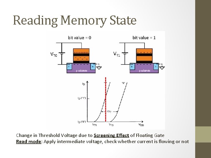
Reading Memory State Change in Threshold Voltage due to Screening Effect of Floating Gate Read mode: Apply intermediate voltage, check whether current is flowing or not

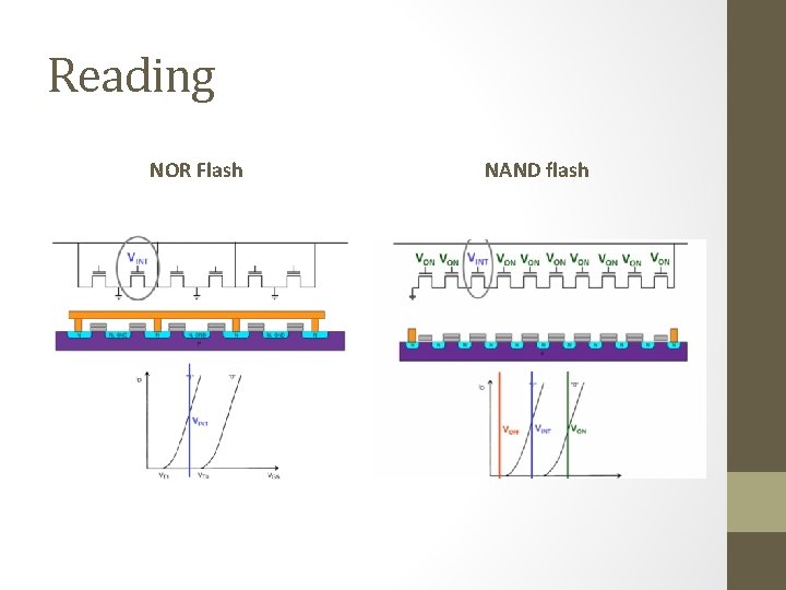
Reading NOR Flash NAND flash

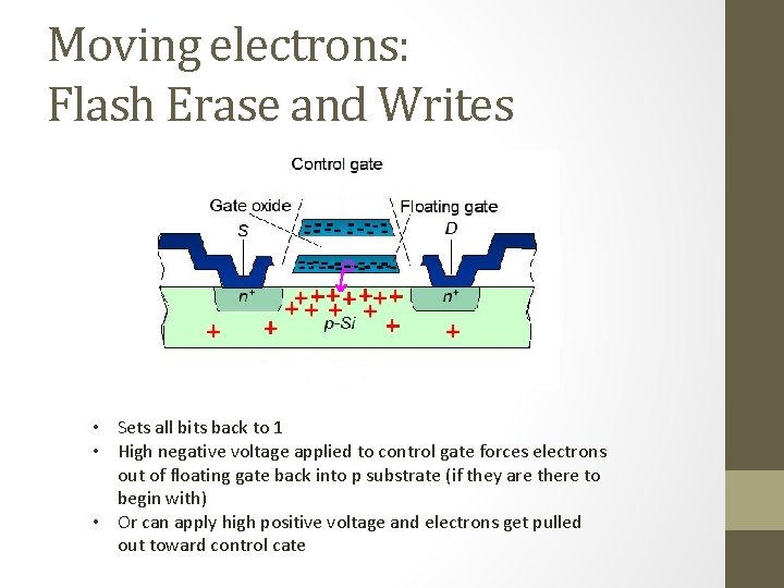
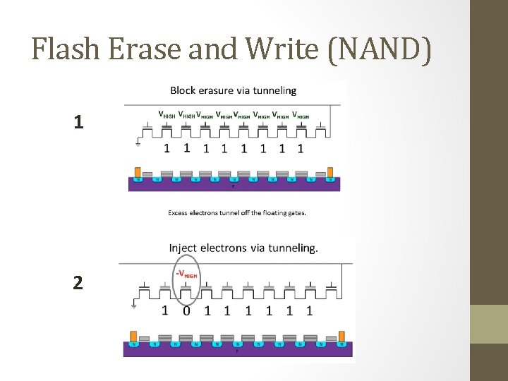
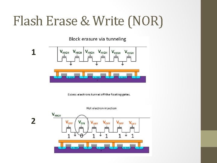
Moving electrons: Flash Erase and Writes • Sets all bits back to 1 • High negative voltage applied to control gate forces electrons out of floating gate back into p substrate (if they are there to begin with) • Or can apply high positive voltage and electrons get pulled out toward control cate

Flash Erase and Write (NAND) 1 2

Flash Erase & Write (NOR) 1 2

Voila – Non-volatile flash memory stick and SD card Limitations: Erase cycles are damaging to the MOSFET structures Partial solution: Wear leveling; newer devices use lower voltages

Microcontrollers & Memory Arduino Uno R 3 Teensy 3. 6 Arduino Uno Teensy 3. 6 Flash 32 k. B 1 MB = 1000 k. B RAM 2 k. B 256 k. B

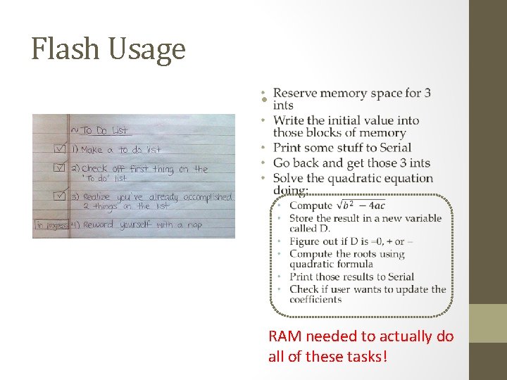
Flash Usage • RAM needed to actually do all of these tasks!

RAM usage • Stack: space for stuff the MCU knows is coming – defined in functions and interrupts • Heap: space for stuff that the MCU doesn’t know is coming (dynamic allocation) Figure 1. SRAM memory usage summary. Image credit: Adafruit. com

Citations/Image Sources • http: //www. learnabout-electronics. org/fet_01. php (JFETs) • https: //volga. eng. yale. edu/teaching-resources/flash-drives/methods -and-materials https: //www. electronics-tutorials. ws/transistor/tran_5. html • https: //www. electronics-tutorials. ws/transistor/tran_6. html (MOSFT operation) • http: //www. electronics-tutorials. ws/transistor/tran_7. html (MOSFET motor control) • http: //www. engadget. com/2011/10/31/engadget-primed-ssds-andyou/ • https: //www. youtube. com/watch? v=msi 5 GDz 9 JIw (hyperscience youtube channel – reading flash contents) • https: //www. youtube. com/watch? time_continue=854&v=s 7 JLXs 5 es 7 I (great summary of Flash memory construction and operation)