Field Effect Transistors FETs EMT 116 Electronic Devices
 EMT 116 Electronic Devices")


 is a type of FET that operates")


, gm, is defined as the change")


")

 a unipolar device (b) a voltage-controlled device (c) a")
 gate and drain (b)")
 the gate-to-source pn junction reverse-biased (b) the")
")
 cutoff and saturation (b)")
 the drain current with the source shorted (b) the drain")
 the gate-to-source bias voltage")
 at its widest point (b) completely")
")
 lower input impedance (B) higher")
 Current controlled device with high input resistance (B) Voltage")


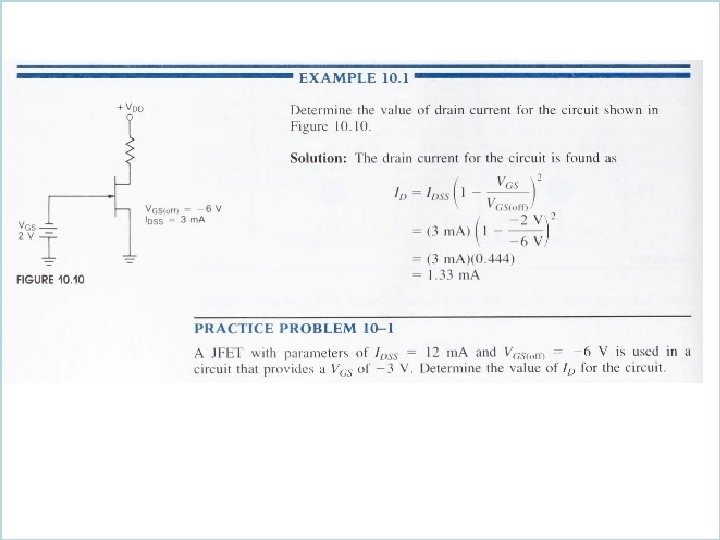
 Calculate VGS")

 (b) Figure 6 -14: (a) An n-channel JFET with voltagedivider")


- Slides: 58
Field Effect Transistors (FETs) EMT 116 Electronic Devices
Introduction BJT FET 3 terminals: Base, Collector, Emitter 3 terminals: Gate, Source, Drain Current-controlled device Voltage-controlled source device Input current flowing into the Base terminal to control the output Collector current of the transistor Input voltage between gate and source control the output drain current of the transistor Bipolar device- use both holes and electrons as current carrier Unipolar device-the current is made of either electron or hole carrier. Major advantage over BJT is high input resistance
1. The N-channel JFET's channel is doped with donor impurities meaning that the flow of current through the channel is in the form of electrons (hence the term Nchannel) 2. The P-channel JFET's channel is doped with acceptor impurities meaning that the flow of current through the channel is in the form of holes. (hence the term P-channel) 3. N-channel JFET's have a greater channel conductivity (lower resistance) than their equivalent P-channel JFET, since electrons have a higher mobility through a conductor compared to holes. 4. This makes the N-channel JFET's a more efficient conductor compared to their P-channel counterparts.
JFET symbols JFET has three terminals, which are GATE, DRAIN and SOURCE. GATE: use to control the flow of carrier from source to drain SOURCE: terminal that emits carrier DRAIN: terminal that receives carrier The schematic symbols for both n-channel and p-channel JFETs are shown in Figure below. The arrow on the gate points “in” for n-channel and “out” for p-channel.
JFET structure JFET (junction field effect transistor) is a type of FET that operates with a reverse-biased p-n junction to control current in a channel. Depending on their structure, JFETs fall into either of two categories, nchannel and p-channel, as shown in Figure below.
JFET basic operation Figure below shows dc bias voltage applied to an nchannel JFET. VGG sets the reverse-bias voltage between the gate and source and VDD provides a drain-to-source voltage and supplies current from drain to source.
The JFET is always operated with the gatesource p-n junction reverse-biased. Reverse-biasing of the gate-source junction with a negative gate voltage produces a depletion region along the p-n junction, which extends into the nchannel and thus increases its resistance by restricting the channel width.
Operation • The device operation is based on REVERSE-BIASING the pn junction between GATE and CHANNEL. • The depletion region is THIN when VGS=0, providing current path between SOURCE and DRAIN. • -ve voltage applied to GATE increases the thickness of the depletion region, hence n-channel becomes smaller and eventually no current can flow between S and D (i. e. PINCH OFF). The pinch-off voltage is denoted as Vp. • At VGS=0, the channel acts as a resistor when a small +ve VDS is applied. The linear behaviour breaks down as V DS increases, because the channel is PINCHED OFF at drain terminal. If VDS continues to increase, the flowing current becomes saturated.
JFET Characteristic & Parameters Ohmic Region • Between point A and B. • The region where voltage and current relationship follows ohm’s law • ID increase proportionally with VDS • Channel resistance is constant because the depletion region is not large enough to have a significant effect Fig. 6 -5: The drain characteristic curve of a JFET for VGS = 0
Constant-current Area • At point B, ID is maximum for VGS = 0 • The value of constant drain current at which VDS increases continuously above VP is Drain to Source current with gate Shorted, IDSS. • No increase of current as VDS is further increased • The reverse bias voltage from drain to gate produces large depletion region to offset the increase of VDS Pinch-Off Voltage For VGS = 0 V, the value of VDS at which ID becomes constant (point B on the curve) is the pinch-off voltage, VP. Breakdown occurs when ID begins to increase very rapidly with further increase in VDS. It can damage the device.
VGS Controls ID Figure below shows a bias voltage, VGG is connected to gate. Adjusting VGG, VGS can be set to increasingly more negative values and a family of drain characteristic curves is produced.
Notice that ID decreases as VGS is increased to larger negative values due to the narrowing of the channel. Also notice that, for each increase in VGS, the JFET reaches pinch-off (where constant current begins) at values of VDS less than VP.
Cutoff Voltage The value of VGS that makes ID approximately zero is the cutoff voltage, VGS(off), as shown in Figure. VGS(off) and Vp are always equal in magnitude but opposite in sign. This cutoff effect is caused by the widening of the depletion region to a point where it completely closes the channel. Thus, the JFET must be operated between VGS = 0 V and VGS(off). For this range, ID will vary from a maximum of IDSS to a minimum of almost zero.
The basic operation of a p-channel JFET is the same as for an n-channel device except that a p-channel JFET requires a negative VDD and a positive VGS, as illustrated in Figure 6 -9.
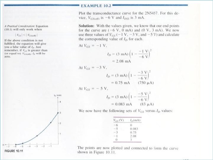
JFET Transfer Characteristic Figure 6 -10 is a general transfer characteristic curve that shows the relationship between VGS and ID known as a transconductance curve. This curve is developed from the drain characteristic curves by plotting values of ID for the values of VGS taken from the family of drain curves at pinch-off. If VGS(off) and IDSS are known, ID can be determined for any VGS. Fig. 6 -10: Example of the development of an n-channel JFET transfer characteristic curve (blue) from the JFET drain characteristic curves (green). (Equation 6. 1)
JFET Forward Transconductance The forward transconductance (transfer conductance), gm, is defined as the change of drain current (ΔID) for a given change in gate-to-source voltage (ΔVGS). It is expressed as (Equation 6. 2) * has the unit of siemens (S). gm is important in FET amplifiers as a major factor in determining the voltage gain.
From the curve, gm of the device is at maximum when VGS = 0. The value of gm at VGS = 0 is always given in the manufacturer data sheet of the device, which is denoted as gmo Fig. 6 -11: gm varies depending on the bias point (VGS).
If gm 0 is given, gm for a given VGS can be calculated by using equation 6. 3 (Equation 6. 3) Equation 6. 3 can be derived from Equation 6. 2 by differentiating ID with respect to VGS i. e. d. ID/d. VGS
Comparing Equation 6. 2 and Equation 6. 3, gmo shall be (Equation 6. 4) Thus, given the values of IDSS and VGS(off), the transconductance of the device at VGS = 0 can be determined. From Equation 6. 1 and Equation 6. 3, transconductance gm can be expressed as (Equation 6. 5)
Input Resistance and Capacitance Due to a JFET operates with its gate-source junction reverse-biased, the input resistance at the gate is very high. This high input resistance is one advantage of the JFET over the BJT. Input resistance can be determined using the following question:
1. The JFET is (a) a unipolar device (b) a voltage-controlled device (c) a current-controlled device (d) answers (a) and (c) (e) answers (a) and (b) Ans: e
2. The channel of a JFET is between the (a) gate and drain (b) drain and source (c) gate and source (d) input and output Ans: b
3. A JFET always operates with (a) the gate-to-source pn junction reverse-biased (b) the gate-to-source pn junction forward-biased (c) the drain connected to ground (d) the gate connected to the source Ans: a
4. For VGS 0 V, the drain current becomes constant when VDS exceeds (a) cutoff (b) VDD (c) VP (d) 0 V Ans: C
5. The constant-current region of a FET lies between (a) cutoff and saturation (b) cutoff and pinch-off (c) 0 and IDSS (d) pinch-off and breakdown Ans: d
6. IDSS is (a) the drain current with the source shorted (b) the drain current at cutoff (c) the maximum possible drain current (d) the midpoint drain current Ans: C
7. Drain current in the constant-current region increases when (a) the gate-to-source bias voltage decreases (b) the gate-to-source bias voltage increases (c) the drain-to-source voltage increases (d) the drain-to-source voltage decreases Ans: a
8. At cutoff, the JFET channel is (a) at its widest point (b) completely closed by the depletion region (c) extremely narrow (d) reverse-biased Ans: b
9. Pinch-off voltage VP for an FET is the drain voltage at which (A) significant drain current starts flowing (B) drain current becomes zero (C) all free charges get removed from the channel (D) avalanche break down takes place Ans: C
10. Compared to bipolar transistor, a JFET has (A) lower input impedance (B) higher voltage gain (C) higher input impedance and high voltage gain (D) higher input impedance and low voltage gain Ans: D
11. JFET is a (A) Current controlled device with high input resistance (B) Voltage controlled device with high input resistance (C) Current Controlled Current Source (CCCS) (D) Voltage Controlled Voltage Source (VCVS) Ans: B
TRUE / FALSE QUIZ 1. The JFET always operates with a reverse-biased gate-to-source pn junction. 2. The channel resistance of a JFET is a constant. 3. The gate-to-source voltage of an n-channel JFET must be negative. 4. ID becomes zero at the pinch-off voltage. 5. VGS has no effect on ID. 6. VGS(off) and Vp are always equal in magnitude but opposite in polarity. 7. Forward transconductance is the change in drain voltage for a given change in gate voltage.
8. The relationship between gm and VGS in an FET is linear 9. An n-channel enhancement mode MOSFET (EMOSFET) has a negative threshold voltage (VT) 10. A JFET and a MOSFET can be used as a resistor whose resistance is controlled by the VGS, when VGS-VP > VDS 11. If we have an application that requires very high input impedance, then we most probably use a JFET transistor 12. A BJT is a current-controlled device whereas JFETs are voltage-controlled devices.
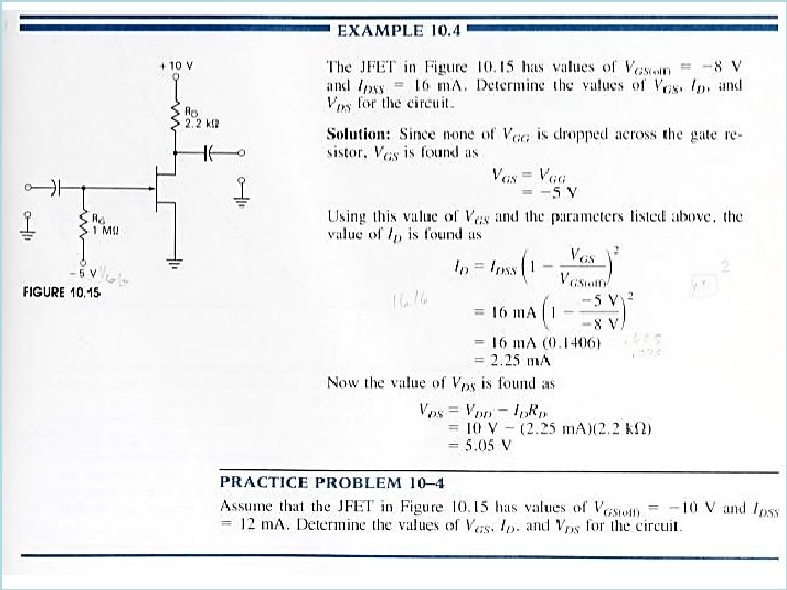
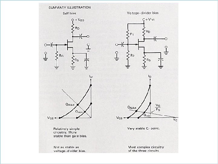
JFET Biasing Just as with BJT, the purpose of JFET biasing is to select the proper dc gate-to-source voltage to establish a desired value of drain current and thus, a proper Q-point. Three types of bias are self-bias, voltagedivider bias, and current-source bias. v Self-Bias Using the self bias arrangements shown in Figure 6 -12, JFET can be operated with the gate-source junction is reverse-biased. The gate resistor, RG, does not affect the bias because it has essentially no voltage drop across it; and therefore the gate remains at 0 V. RG is necessary only to force the gate to be at 0 V and to isolate an ac signal from ground in amplifier applications. Fig. 6 -12: Self-biased JFETs (IS = ID in all FETs).
For n-channel JFET requiring a negative VGS, the gate-to-source voltage is 6 -7 Since VG = 0 and IS = ID, then V S = I D R S. For p-channel JFET requiring a positive VGS, the gate-to-source voltage is 6 -8
Keeping in mind that analysis of p-channel JFET is the same with that of n-channel JFET except for opposite-polarity voltages, drain voltage with respect to ground is determined as follows: 6 -9 Since VS = IDRS, the drain-to-source voltage is 6 -10
Example 1 Find VDS and VGS for the circuit in this figure.
For VDS: For VGS:
Determine VDS and VGS when ID = 8 m. A. Ans: VS = 3. 12 V VD = 5. 12 V VDS = 2 V VGS = -3. 12 V
Graphical Analysis of a Self-Biased JFET The transfer characteristic curve of a JFET and certain parameters can be used to determine the Q-point (ID and VGS) of a self-biased circuit. Fig. 6 -20: Self-biased JFETs and its transfer characteristic curve
To determine Q point of the circuit in Fig 6 -20, 1) Calculate VGS when ID=0 2) Calculate VGS when ID=IDSS 3) Draw load line with these two points to find Q point = (-2. 3, 5. 07) ID = 5. 07 m. A, VGS = -2. 3 V
Example 2 Determine the Q-point for the JFET circuit in figure below.
v Voltage-Divider Bias (a) (b) Figure 6 -14: (a) An n-channel JFET with voltagedivider bias and (b) dc load line (red) for the JFET. The gate to source voltage is 6 -12 The gate voltage is calculated using the voltage-divider formula: 6 -13
The source voltage is determined using the following formula: 6 -14 Since in this case IS = ID. Meanwhile the drain current can be expressed as 6 -15 The other expression for the drain current is 6 -16
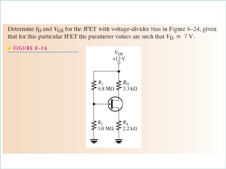
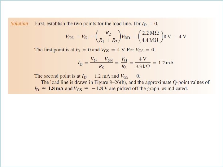
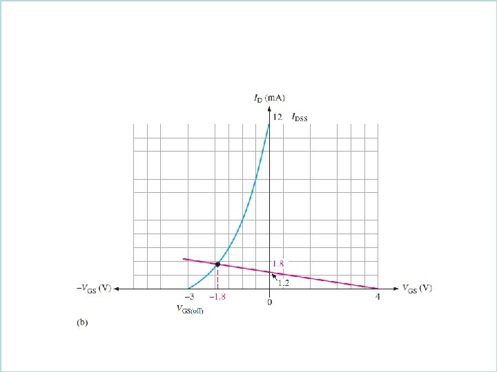
Given VD = 7 V For ID: For VGS:
Given that VD = 6 V, determine the Q point. Ans: ID = 2. 353 m. A VGS = -4. 29 V
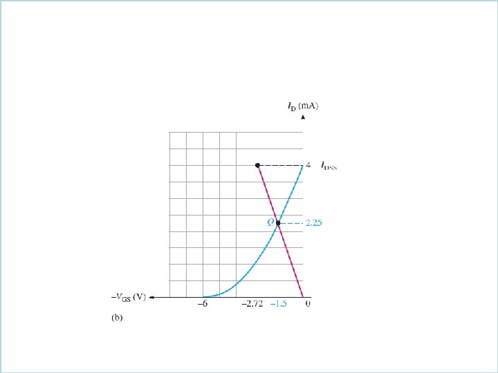
Graphical Analysis of a JFET with Voltage-Divider Bias The transfer characteristic curve of a JFET and certain parameters can be used to determine the Q-point (ID and VGS) of a voltage-divider-biased circuit. Fig. 6 -26: Voltage divider-biased JFETs and its transfer characteristic curve
Q-Point Stability Figure 6 -15 illustrates Q-point stability for a self-biased JFET and for a JFET with voltage divider bias. With voltage-divider bias, the change in ID between minimum and maximum Q-points is reduced because the slop of load line is less than for self-bias. Figure 6 -15.