JFET Junction Field Effect Transistor Introduction FET o

 o Field-effect transistor (FET) are important devices such as BJTs o Also")


 § FET JFET n-Channel JFET p-Channel JFET")
 o High input impedance (M ) (Linear")


 between")

 between")


.")

")


 and ID (output")


")
")

")
")

- Slides: 37
JFET Junction Field Effect Transistor
Introduction (FET) o Field-effect transistor (FET) are important devices such as BJTs o Also used as amplifier and logic switches o What is the difference between JFET and BJT?
BJT is Current-controlled
FET is Voltage-controlled
Types of Field Effect Transistors (The Classification) § FET JFET n-Channel JFET p-Channel JFET MOSFET (IGFET) Enhancement MOSFET n-Channel EMOSFET p-Channel EMOSFET Depletion MOSFET n-Channel DMOSFET p-Channel DMOSFET
Introduction. . (Advantages of FET over BJT) o High input impedance (M ) (Linear AC amplifier system) o Temperature stable than BJT o Smaller than BJT o Can be fabricated with fewer processing o BJT is bipolar – conduction both hole and electron o FET is unipolar – uses only one type of current carrier o Less noise compare to BJT o Usually use as an Amplifier and logic switch
Disadvantages of FET o Easy to damage compare to BJT
Junction field-effect transistor. . o There are 2 types of JFET n n-channel JFET n p-channel JFET o Three Terminal n Drain – D n Gate -G n Source – S
SYMBOLS Drain Gate Source n-channel JFET Source p-channel JFET
N-channel JFET o N channel JFET: n Major structure is n-type material (channel) between embedded p-type material to form 2 pn junction. n In the normal operation of an n-channel device, the Drain (D) is positive with respect to the Source (S). Current flows into the Drain (D), through the channel, and out of the Source (S) n Because the resistance of the channel depends on the gate-to-source voltage (VGS), the drain current (ID) is controlled by that voltage
N-channel JFET. .
P-channel JFET o P channel JFET: n Major structure is p-type material (channel) between embedded n-type material to form 2 p-n junction. n Current flow : from Source (S) to Drain (D) n Holes injected to Source (S) through ptype channel and flowed to Drain (D)
P-channel JFET. .
Water analogy for the JFET control mechanism
JFET Characteristic for VGS = 0 V and 0<VDS<|Vp| o To start, suppose VGS=0 o Then, when VDS is increased, ID increases. Therefore, ID is proportional to VDS for small values of VDS o For larger value of VDS, as VDS increases, the depletion layer become wider, causing the resistance of channel increases. o After the pinch-off voltage (Vp) is reached, the ID becomes nearly constant (called as ID maximum, IDSS-Drain to Source current with Gate Shorted)
JFET for VGS = 0 V and 0<VDS<|Vp| Channel becomes narrower as VDS is increased
Pinch-off (VGS = 0 V, VDS = VP).
ID versus VDS for VGS = 0 V and 0<VDS<|Vp| JFET Characteristic Curve
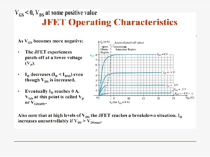
JFET for (Application of a negative voltage to the gate of a JFET )
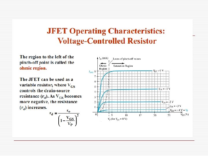
JFET Characteristic Curve. . o For negative values of VGS, the gate-to-channel junction is reverse biased even with VDS=0 o Thus, the initial channel resistance of channel is higher. o The resistance value is under the control of VGS o If VGS = pinch-off voltage(VP) The device is in cutoff (VGS=VGS(off) = VP) o The region where ID constant – The saturation/pinchoff region o The region where ID depends on VDS is called the linear/ohmic region
p-Channel JFET
p-Channel JFET characteristics with IDSS = 6 m. A and VP = +6 V.
Characteristics for n-channel JFET
Characteristics for p-channel JFET + + + P
Transfer Characteristics The input-output transfer characteristic of the JFET is not as straight forward as it is for the BJT. In BJT: I C= I B which is defined as the relationship between IB (input current) and IC (output current).
Transfer Characteristics. . In JFET, the relationship between VGS (input voltage) and ID (output current) is used to define the transfer characteristics. It is called as Shockley’s Equation: VP=VGS (OFF) The relationship is more complicated (and not linear) As a result, FET’s are often referred to a square law devices
Transfer Characteristics… o Defined by Shockley’s equation: o Relationship between ID and VGS. o Obtaining transfer characteristic curve axis point from Shockley: n When VGS = 0 V, ID = IDSS n When VGS = VGS(off) or Vp, ID = 0 m. A
Transfer Characteristics JFET Transfer Characteristic Curve JFET Characteristic Curve
Exercise 1 Sketch the transfer defined by IDSS = 12 m. A dan VGS(off) = - 6 VGS 0 0. 3 Vp 0. 5 Vp Vp ID IDSS/2 IDSS/4 0 m. A
Exercise 1 Sketch the transfer defined by IDSS = 12 m. A dan VGS(off) = Vp= - 6 IDSS VGS =0. 3 VP VGS =0. 5 VP IDSS/2 IDSS/4
Answer 1
Exercise 2 Sketch the transfer defined by IDSS = 4 m. A dan VGS(off) = 3 V VGS 0 0. 3 Vp 0. 5 Vp Vp ID IDSS/2 IDSS/4 0 m. A
Exercise 2 Sketch the transfer defined by IDSS = 4 m. A dan VGS(off) = 3 V IDSS/2 IDSS/4 VGS =0. 3 VP VP VGS =0. 5 VP
Answer 2