ChapterIV Field Effect Transistor FET Contents Junction Field

- Slides: 37

Chapter-IV Field Effect Transistor (FET)

Contents �Junction Field Effect Transistors: Structure, principle of operation, characteristics, comparison with BJT. �MOSFET: Structure, principle of operation of Enhancement type MOSFET, Current voltage characteristics, Depletion type MOSFET. �Principle UJT, SCR. of operation of Photo transistor,

Field Effect Transistor (FET) �Field Effect Transistor (FET) is a three terminal semiconductor device in which the output current is controlled by an electric field (voltage). There fore it is called voltage controlled device. The conduction of current in the device is only by majority carriers (either holes or electrons) and hence it is said to be a unipolar device.

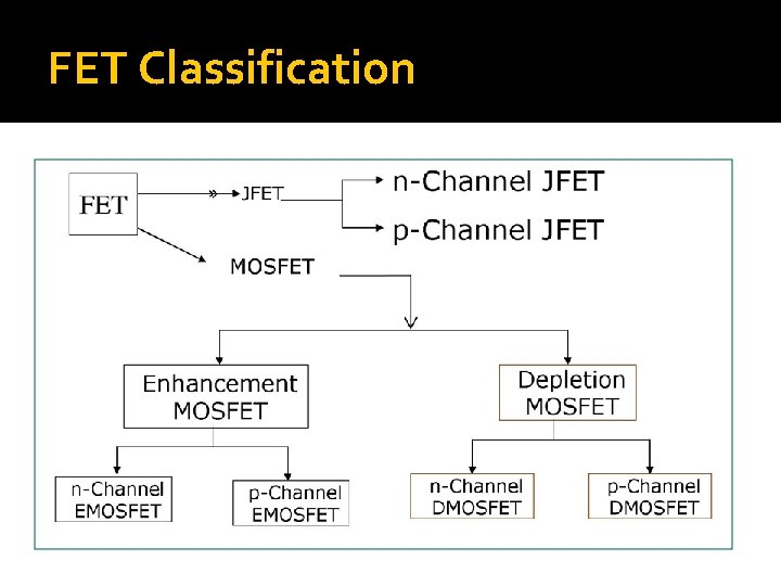
FET Classification

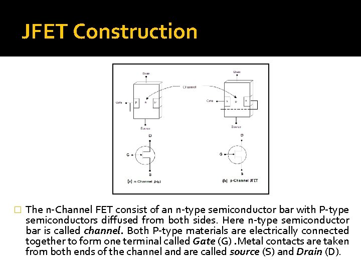
JFET Construction � The n Channel FET consist of an n type semiconductor bar with P type semiconductors diffused from both sides. Here n type semiconductor bar is called channel. Both P type materials are electrically connected together to form one terminal called Gate (G). Metal contacts are taken from both ends of the channel and are called source (S) and Drain (D).

JFET Operation

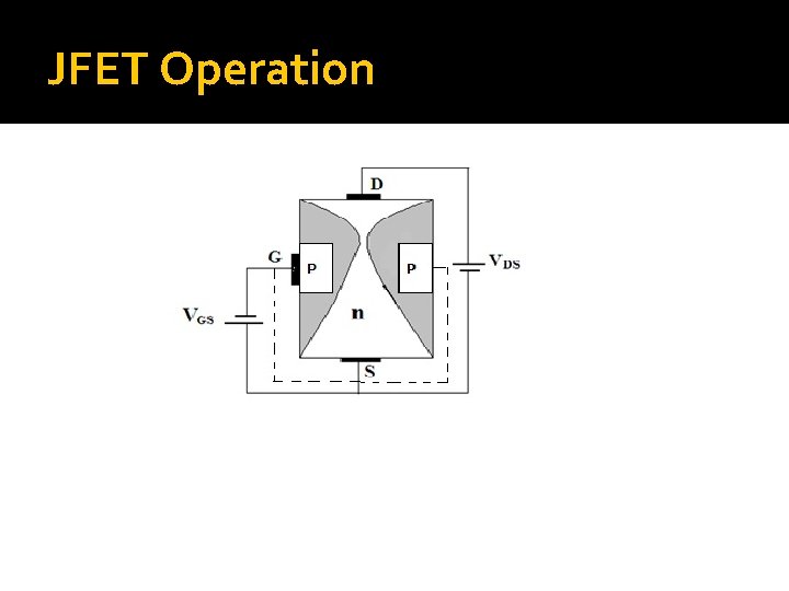
JFET Operation � Operation with gate to source voltage = 0 � If an n channel JFET , the gate to source voltage is kept zero, due to the positive drain to source voltage electrons will start flowing from source to drain. This current is called as drain current. � As the channel has some finite resistance it will cause some voltage drop across the channel. Hence the depletion region of the p n junction starts increasing and penetrates more into the n type material as it is lightly doped. Due to this the width of the channel available for conduction is reduced. The penetration of the depletion region into the n type region depends on the reverse bias voltage. Maximum drain current ID(MAX) will flow through the device when the channel is widest i. e. when VGS is zero.

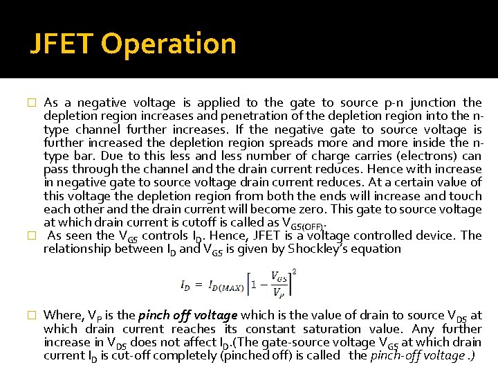
JFET Operation As a negative voltage is applied to the gate to source p n junction the depletion region increases and penetration of the depletion region into the n type channel further increases. If the negative gate to source voltage is further increased the depletion region spreads more and more inside the n type bar. Due to this less and less number of charge carries (electrons) can pass through the channel and the drain current reduces. Hence with increase in negative gate to source voltage drain current reduces. At a certain value of this voltage the depletion region from both the ends will increase and touch each other and the drain current will become zero. This gate to source voltage at which drain current is cutoff is called as VGS(OFF). � As seen the VGS controls ID. Hence, JFET is a voltage controlled device. The relationship between ID and VGS is given by Shockley’s equation � � Where, VP is the pinch off voltage which is the value of drain to source VDS at which drain current reaches its constant saturation value. Any further increase in VDS does not affect ID. (The gate source voltage VGS at which drain current ID is cut off completely (pinched off) is called the pinch-off voltage. )

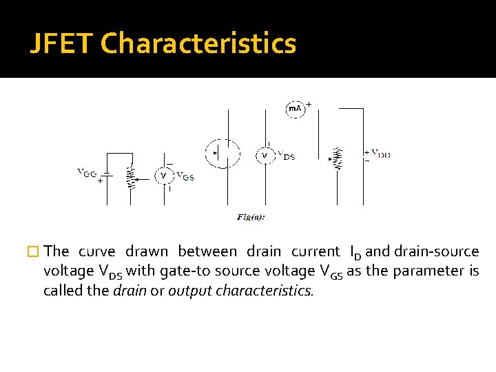
JFET Characteristics � The curve drawn between drain current ID and drain source voltage VDS with gate to source voltage VGS as the parameter is called the drain or output characteristics.

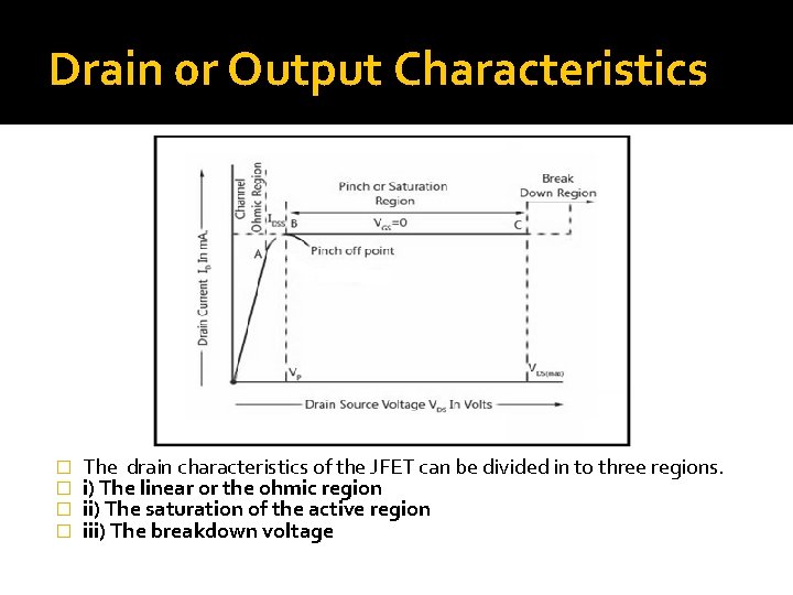
Drain 0 r Output Characteristics � � The drain characteristics of the JFET can be divided in to three regions. i) The linear or the ohmic region ii) The saturation of the active region iii) The breakdown voltage

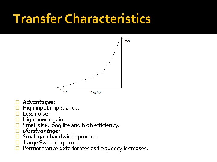
Transfer Characteristics � � � � � Advantages: High input impedance. Less noise. High power gain. Small size, long life and high efficiency. Disadvantage: Small gain bandwidth product. Large Switching time. Permormance deteriorates as frequency increases.

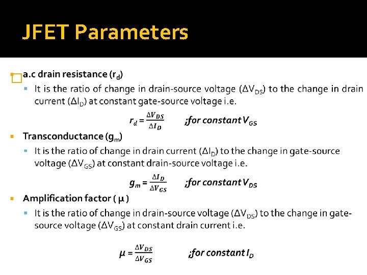
JFET Parameters �

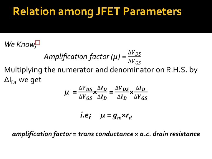
Relation among JFET Parameters �

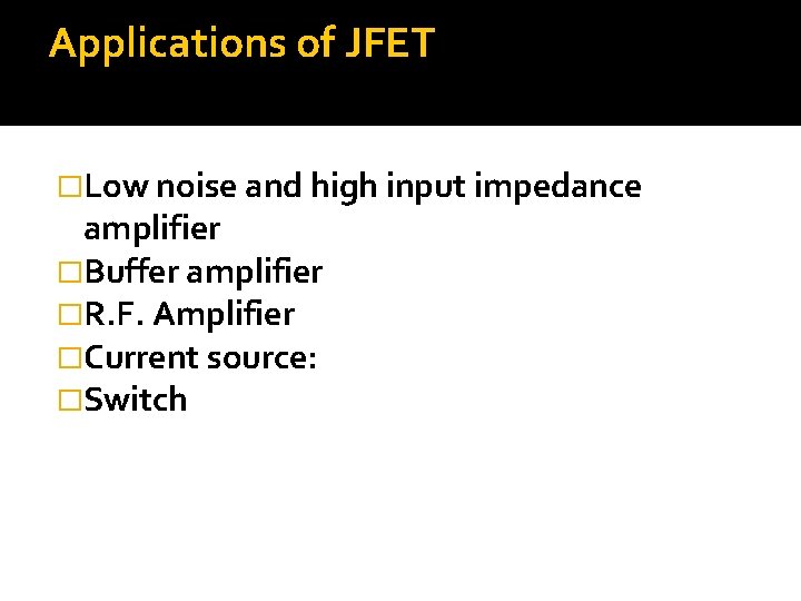
Applications of JFET �Low noise and high input impedance amplifier �Buffer amplifier �R. F. Amplifier �Current source: �Switch

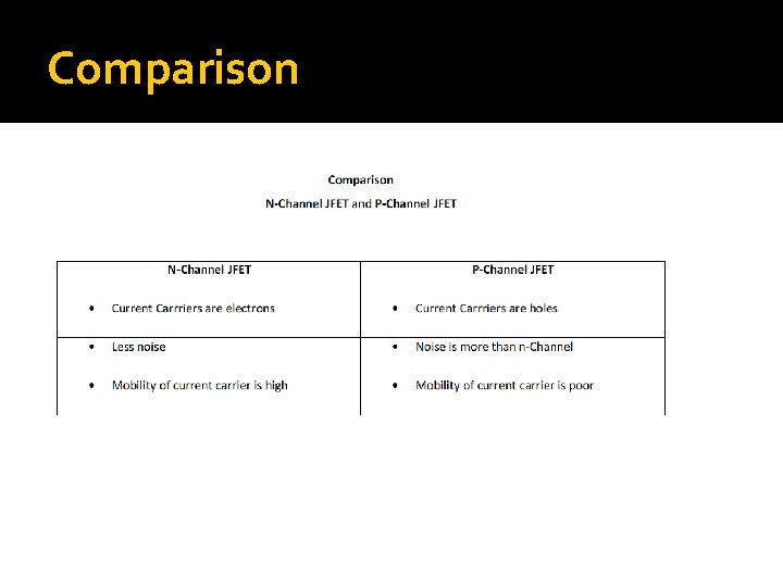
Comparison

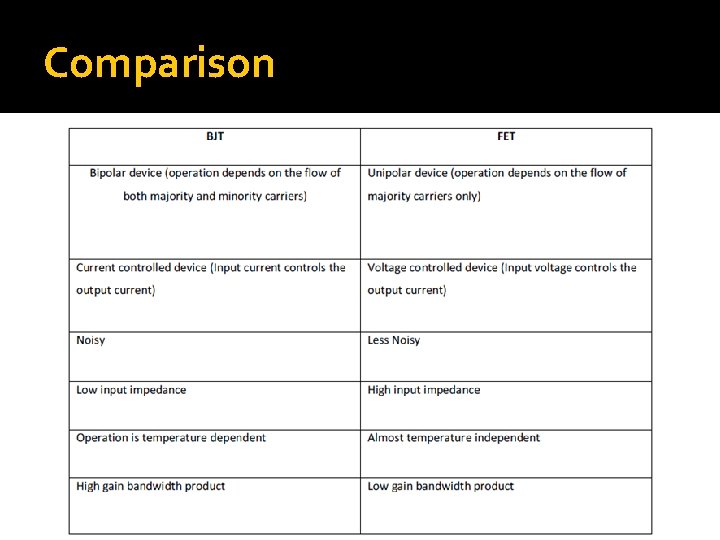
Comparison

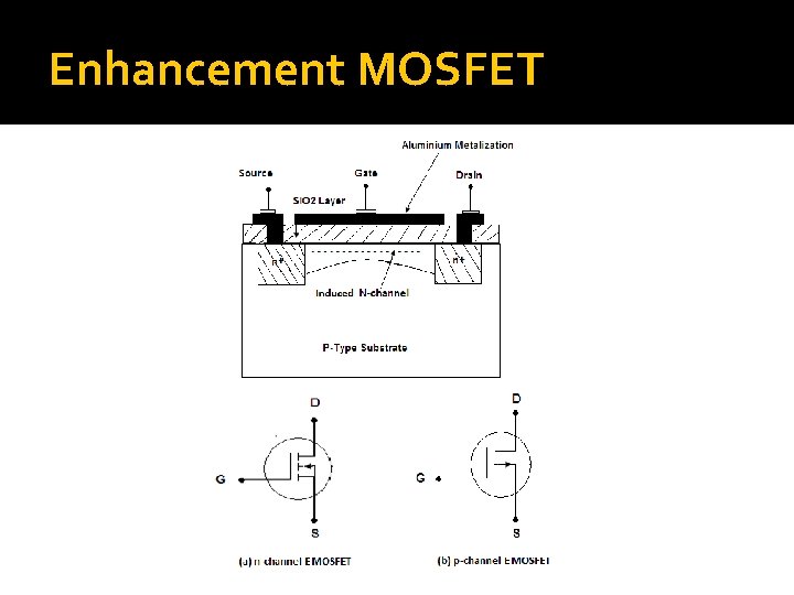
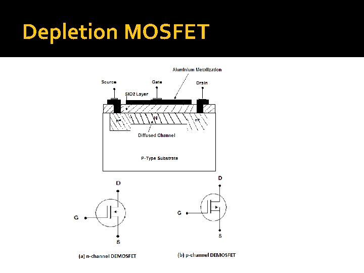
MOSFET �There are two basic forms of MOSFET. Enhancement MOSFET. Depletion MOSFET.

Enhancement MOSFET

Depletion MOSFET

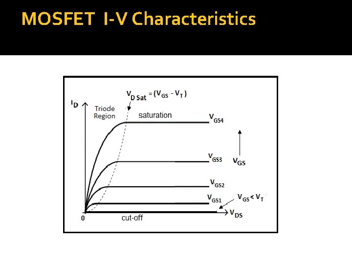
MOSFET I-V Characteristics

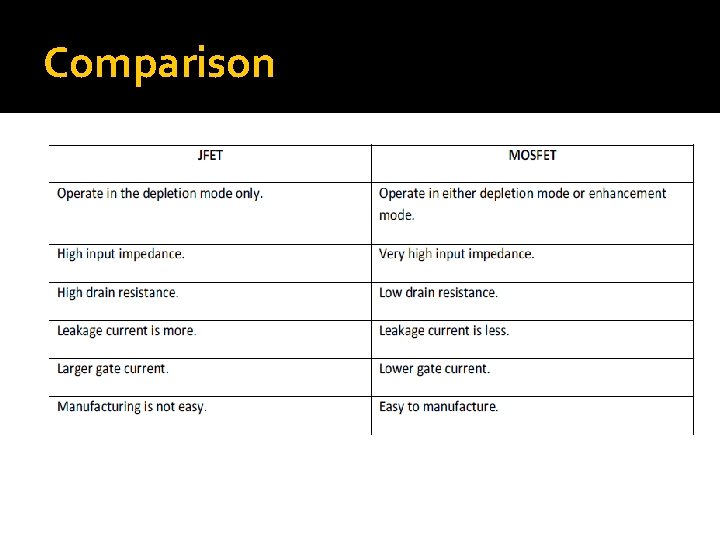
Comparison

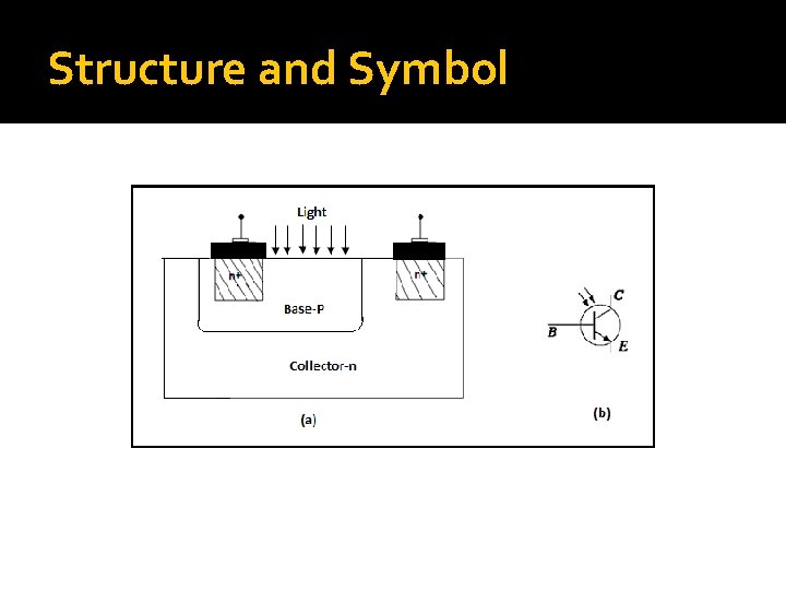
Photo transistor �Photo transistor is nothing but an ordinary bi poplar transistor in which the base region is exposed to the illumination. �It is available in both the P N P and N P N types having different configurations like common emitter, common collector and common base. Common emitter configuration is generally used.

Structure and Symbol

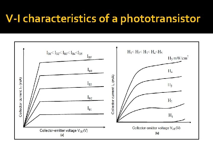
V-I characteristics of a phototransistor

Advantages, Disadvantages and Applications Advantages of Photo transistors: Phototransistors produce a higher current than photo diodes. Phototransistors are relatively inexpensive, simple, and small enough to fit several of them onto a single integrated computer chip. � Phototransistors are very fast and are capable of providing nearly instantaneous output. � � � Disadvantages of Photo transistors: Phototransistors that are made of silicon are not capable of handling voltages over 1, 000 Volts. � Phototransistors are also more vulnerable to surges and spikes of electricity as well as electromagnetic energy. � � � � Applications Punch card readers. Security systems electric controls Computer logic circuitry.

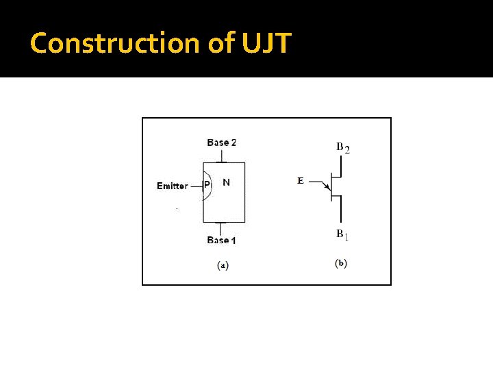
Uni-junction transistor �Uni junction transistor is also known as double base diode because it is a 2 layered, 3 terminal device. It has only one junction so it is called as a uni junction device. The unique characteristic feature of this device is such that when it is triggered, the emitter current increases until it is restricted by an emitter power supply.

Construction of UJT

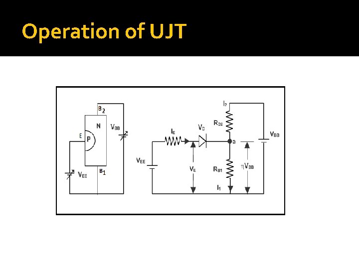
Operation of UJT

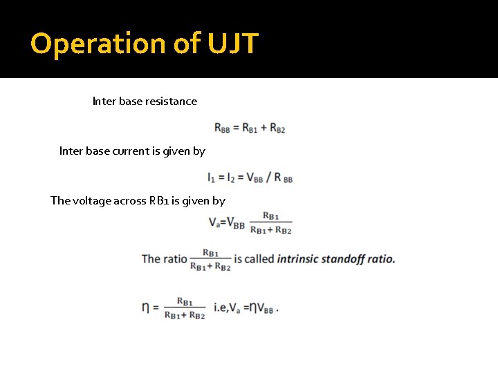
Operation of UJT Inter base resistance Inter base current is given by The voltage across RB 1 is given by

UJT Characteristics

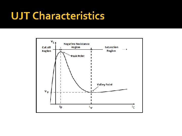
Parameters of UJT � Peak-Point Emitter Current (Ip). It is the emitter current at the peak point. It repre sentsthe minimum current that is required to trigger the (UJT). It is inversely proportional to the inter base voltage VBB. � Valley Point Voltage VV. The valley point voltage is the emitter voltage at the valley point. The valley voltage increases with the increase in inter base voltage VBB. � Valley Point Current IV. The valley point current is the emitter current at the valley point. It increases with the increase in inter base voltage VBB.

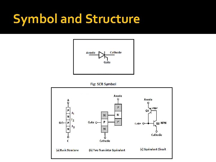
Thyristors (SCRs) �A thyristor is normally four layer three terminal device. Four layers are formed by alternating n – type and p – type semiconductor materials. Consequently there are three p – n junctions formed in the device. �The three terminals of this device are called anode (A), cathode (K) and gate (G) respectively. The gate (G) terminal is control terminal of the device. That means, the current flowing through the device is controlled by electrical signal applied to the gate (G) terminal.

Symbol and Structure

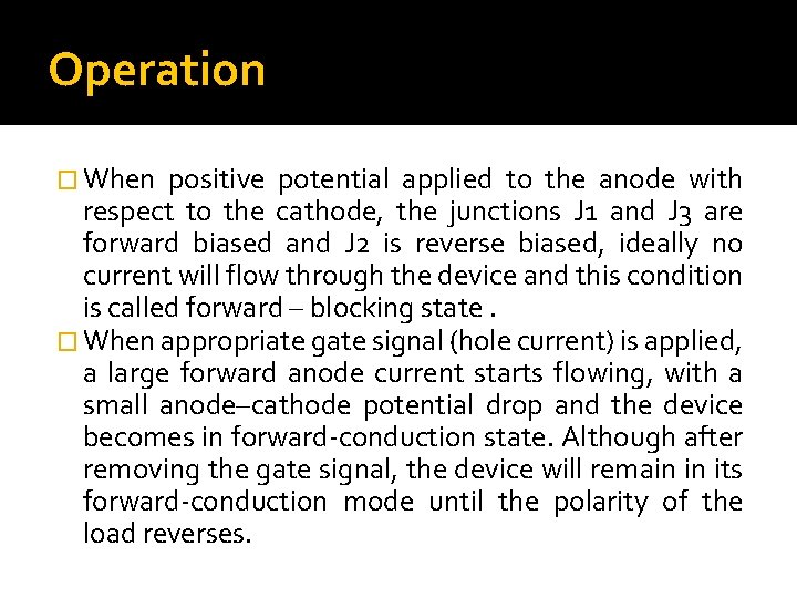
Operation � When positive potential applied to the anode with respect to the cathode, the junctions J 1 and J 3 are forward biased and J 2 is reverse biased, ideally no current will flow through the device and this condition is called forward – blocking state. � When appropriate gate signal (hole current) is applied, a large forward anode current starts flowing, with a small anode–cathode potential drop and the device becomes in forward conduction state. Although after removing the gate signal, the device will remain in its forward conduction mode until the polarity of the load reverses.

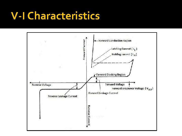
V-I Characteristics

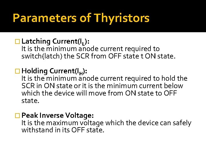
Parameters of Thyristors � Latching Current(IL): It is the minimum anode current required to switch(latch) the SCR from OFF state t ON state. � Holding Current(IH): It is the minimum anode current required to hold the SCR in ON state or it is the minimum current below which the device will move from ON state to OFF state. � Peak Inverse Voltage: It is the maximum voltage which the device can safely withstand in its OFF state.

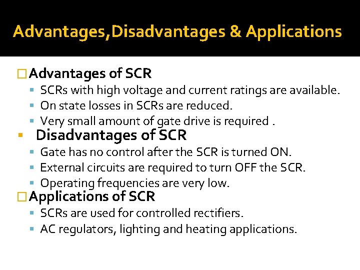
Advantages, Disadvantages & Applications �Advantages of SCRs with high voltage and current ratings are available. On state losses in SCRs are reduced. Very small amount of gate drive is required. Disadvantages of SCR Gate has no control after the SCR is turned ON. External circuits are required to turn OFF the SCR. Operating frequencies are very low. �Applications of SCRs are used for controlled rectifiers. AC regulators, lighting and heating applications.