Field effect transistor Field Effect Transistor FET Types
 Types and Features Here I’m discussing about")


. v is a transistors for constructing integrated circuits.")

 transistors")


 Metal Oxide Semiconductor")


, there is another type of")


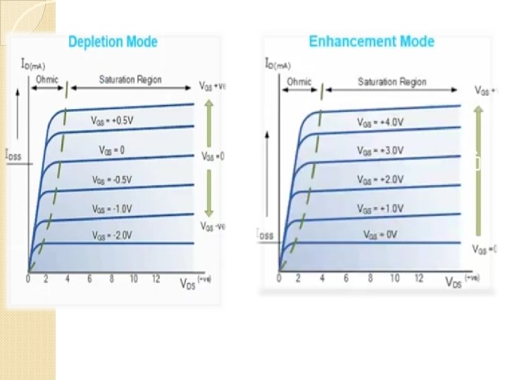
Region VDS < (VGS – VP) The drain current is given by IDS=2 IDSS/V²P")


,")

 SIPMOS-FET It is similar to the VMOS-FET installation according to")


- Slides: 53
Field- effect transistor Field Effect Transistor (FET) Types and Features Here I’m discussing about the topic FET is another semiconductor device like BJT which can be used as switch, amplifier, resistor etc. FET consists of 3 terminals. Drain(D) Source(S) Gate(G) In these 3 terminals, Gate terminal acts as a controlling terminal. We know that a BJT acts as a current controlling device. Like that, FET also acts as a voltage controlling device. Here, the voltage between gate and source controls the drain current. So, it is called as voltage controlled device. FET Features:
Types of FETs: 1. Junction FET 2. MESFET 3. MOSFET Here I am discussing about the topic JFET. Junction FET (JFET): Basically the JFET is classified into 2 types. N-Channel JFET P-Channel JFETN-
N-Channel JFET: When we consider a silicon bar and fabricated n-type at its two ends and heavily doped ptype materials at each side of the bar, the thin region will be remained as observed in figure is channel. Since this channel is in n-type bar this is called as n-channel FET. Here the current is carried by electrons. P-Channel FET: When we consider a silicon bar and fabricated p-type at its two ends and heavily doped ntype materials at each side of the bar, here thin region remained as observed in figure is channel. Since this channel is in n-type bar this is called as p-channel FET. Here the current is carried by holes. Symbols of N-channel JFET and P-channel JFET:
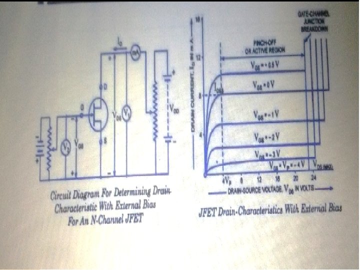
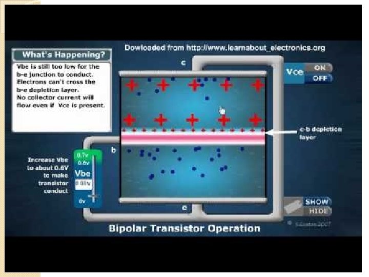
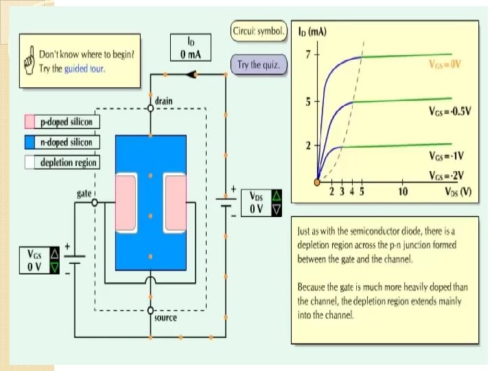
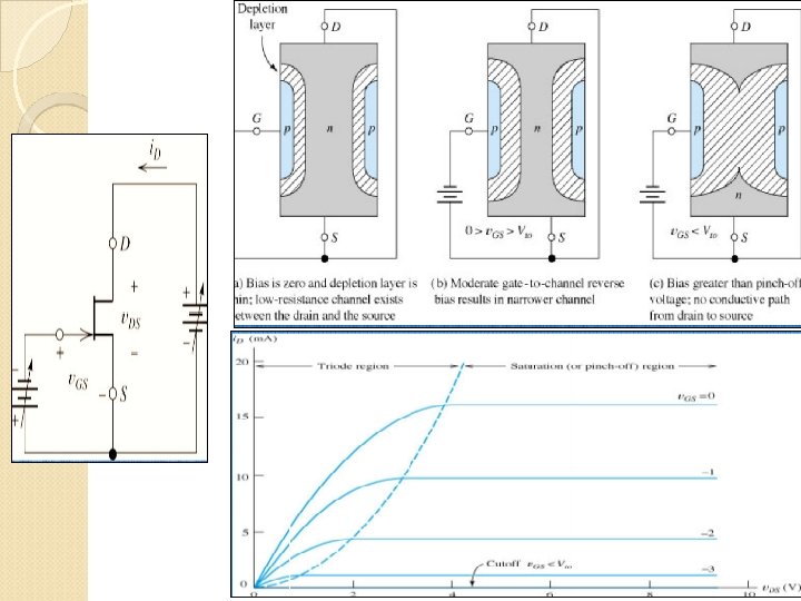
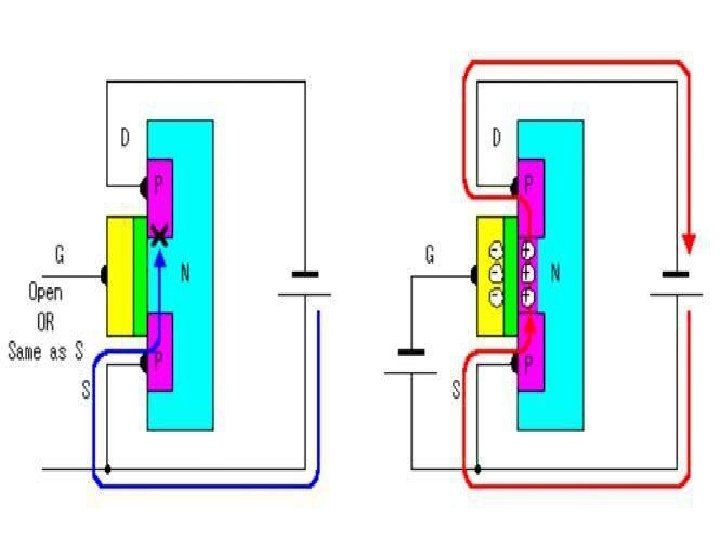
JFET has gate channel junctions under no bias conditions. The result is a depletion region at each junction as shown in figure. Operation: In JFET the p-n junction between source and gate is always kept in reverse biased conditions. Hence, practically in reverse biased conditions the current is less (zero). Consider N-Channel JFET with gate open and supply is applied between gate and source as shown in figure. Due to polarities of applied voltage, the majority carriers start flowing from source to the drain. The majority carriers basically move through the space between the gate regions. This space is known as channel. The width of channel can be
When we connected an N-Channel JFET with the gate directly connected to the source terminal. When drain voltage is applied, a drain current flows through channel. It causes a voltage drop across depletion region to penetrate into channel. Since gate is heavily doped and channel is lightly doped, the width of depletion region is spread into channel.
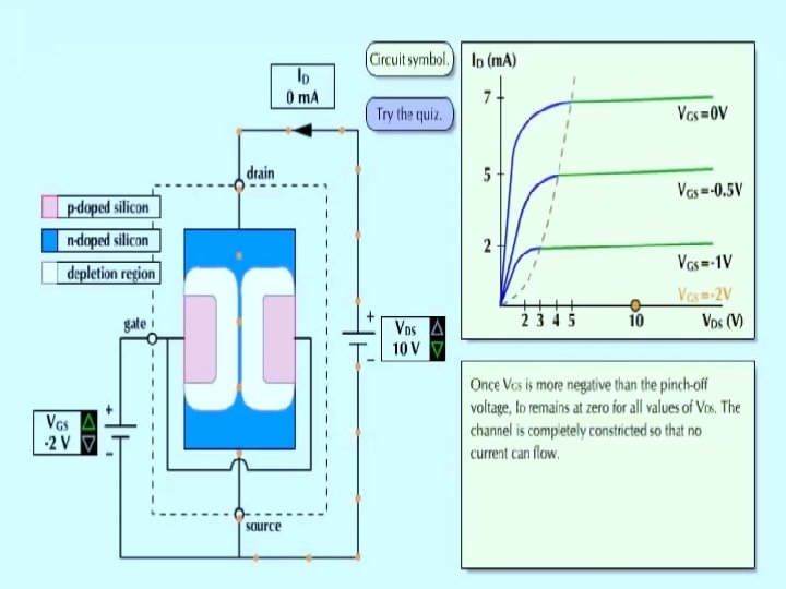
In the same way if we applied less voltage at the gate, we can get the depletion region as shown in figure and if we applied more voltage at the gate, we can get the depletion region which covers the entire channel without any gap. So there will be no current flow from drain to source through channel. The gate to source voltage that produces cutoff is known as cutoff voltage. V-I Charactaristics of N-Channel JFET:
Metal-oxide semiconductor FET (MOSFET
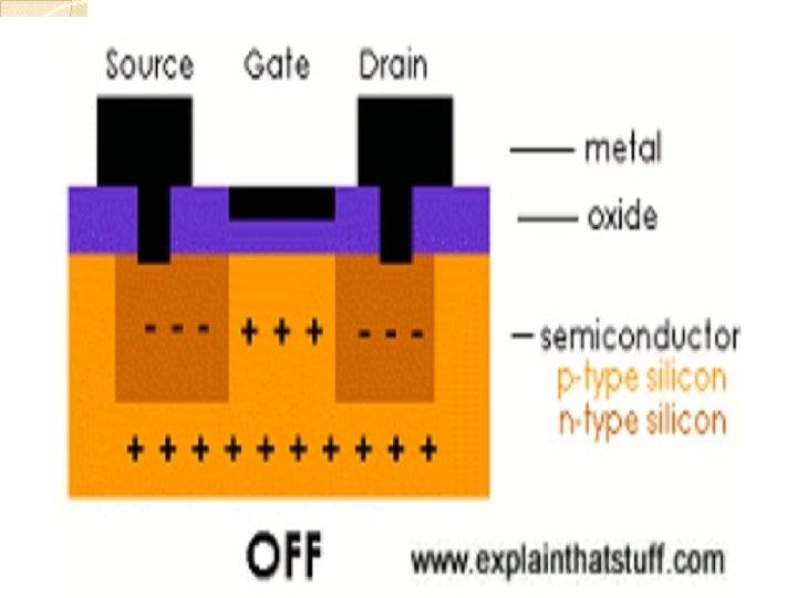
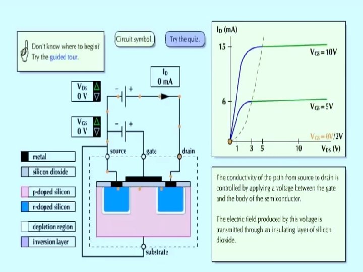
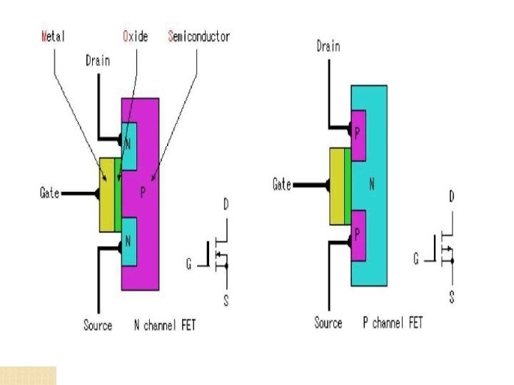
This transistor consists of four pieces ; 1. Substrate : It is either type N as in the right or form P type as the left on the fig. 2. Two areas of two crystals of the same type opposite the bottom layer (Substrate) They represent two parties Drain and source. 3. Layer of oxide (SIO 2) it is non-conductive material of the electric current (dielectric). 4. a layer of metal represents the third party of the transistor which is the gate
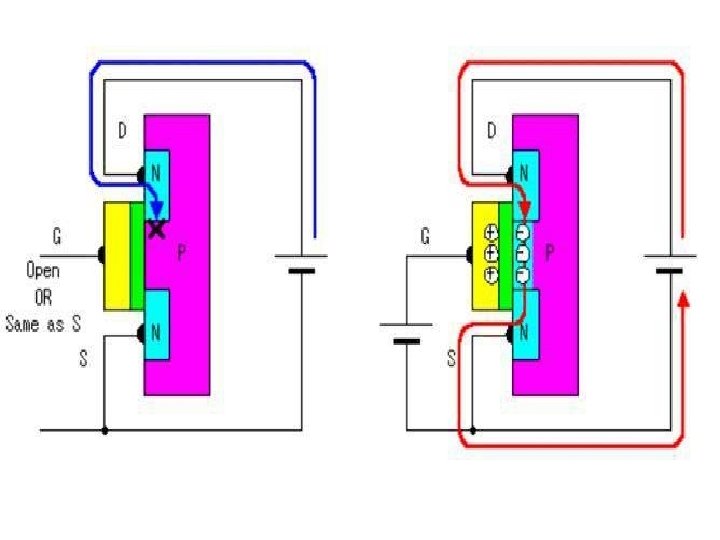
The idea of transistor work 1. If not put voltage on the gate it won’t pass any current between source & drain.
2. In the case when we put positive voltage on the gate the free electrons in the crystals Source & drain was attracted to the positive electric field produced by the gate.
3. In the case when we put negative voltage on the gate Gaps in the source & drain was attracted to the negative electric field produced by the gate
CMOS Complementary Metal Oxide Semiconductor Field Effec It is a circuit that combines between two transistor P & MOSFET one of the most important devices used in the design and construction of integrated Circuits for digital computers
CMOS is (Complementary Metal Oxide Semiconductor). v is a transistors for constructing integrated circuits. v CMOS transistor used for several analog circuits such as • image sensors. • data converters. • Transmitters and receivers for a variety of different communication systems.
q. Noise resistance. q. Minimize energy consumption. q. Its energy is not consumed by heat.
CMOS circuits are constructed in such a way that all P-type metal-oxide-semiconductor (PMOS) transistors must have either an input from the voltage source or from another PMOS transistor. • Similarly, all (NMOS) transistors must have either an input from ground or from another (NMOS) transistor. • The composition of a PMOS transistor creates low resistance between its source and drain contacts when a low gate voltage is applied and high resistance when a high gate voltage is applied. •
v CMOS accomplishes current reduction by complementing every n-channel MOSFET with a pchannel MOSFET and connecting both gates and both drains together. A high voltage on the gates will cause the n-channel MOSFET to conduct and the p-channel MOSFET to not conduct, while a low voltage on the gates causes the reverse.
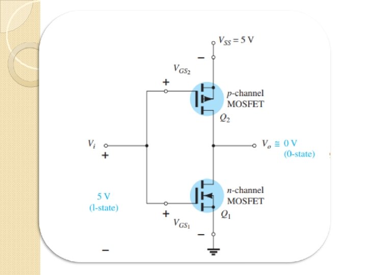
v Use of the CMOS is an Inverter: an inverter is a logic element that “inverts”the applied signal. That is, if the logic levels of operation are 0 V (0 -state) and 5 V (1 -state), an input level of 0 V will result in an output level of 5 V, and vice versa. v. Composition • that both gates are connected to the applied signal and both drain to the output V o. • The source of the p -channel MOSFET (Q 2) is connected directly to the applied voltage VSS. • whereas the source of the n -channel MOSFET (Q 1) is connected to ground.
the application of 5 V at the input should result in approximately 0 V at the output. With 5 V at V i (with respect to ground), VGS 1 = Vi, and Q 1 is “on, ” resulting in a relatively low resistance between drain and source. • When V i and VSS are at 5 V, VGS 2 = 0 V, which is less than the required V T for the device, resulting in an “off” state as shown below • The result is that Q 2 will present a small resistance level, Q 1 a high resistance.
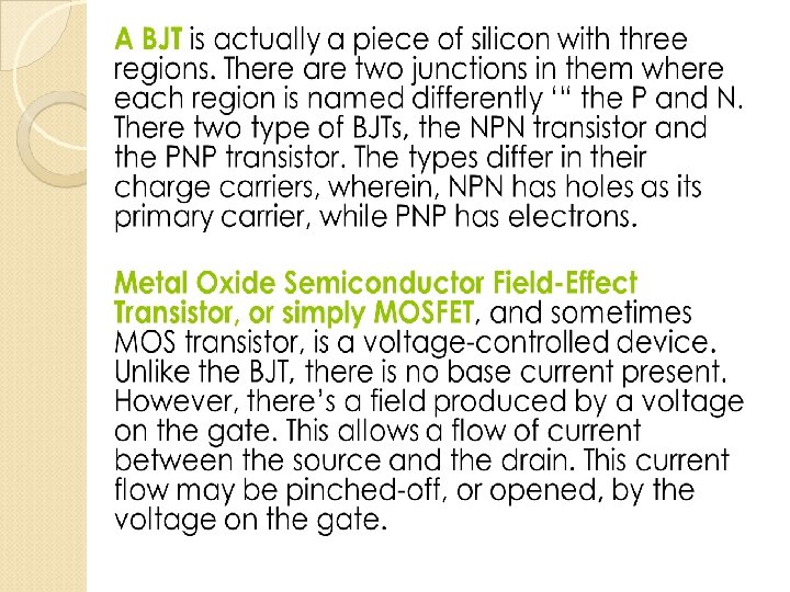
Transistor classifications Classified transistor to two kinds Field Effect Transistor (FET) Metal Oxide Semiconductor FET Junction FET Depletion_ mode N-channel P_ channel Depletion_ mode N-channel Bipolar Junction transistor (BJT) P_ channel NPN Enhanceme nt_mode N-channel P_ channel PNP
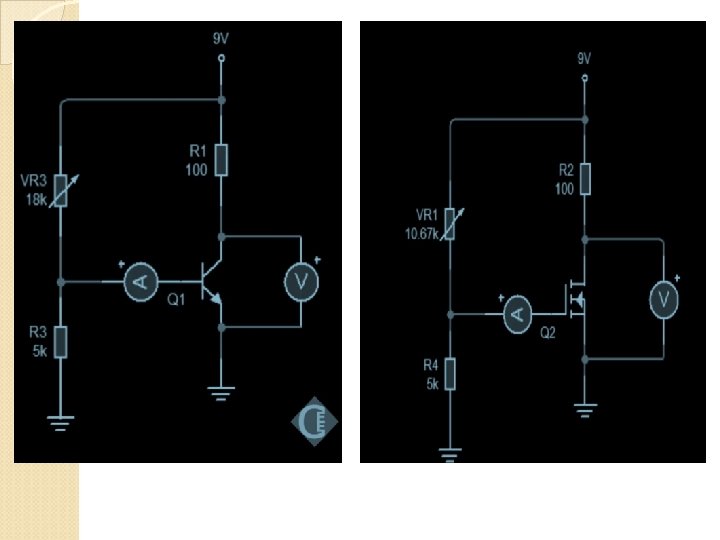
BJT vs MOSFET The transistors BJT and MOSFET are both useful for amplification and switching applications. Yet, they have significantly different characteristics.
An element that can be controlled by the electrical voltage applied to the gate. . 1 The input resistance is so large that the gate doesn’t consume any current for the control of the transistor. . 2 The possibility of damage is very large. . 3 Can be controlled at high frequencies. . 4 Higher price. . 5 Power consumption less (less heat). . 6 It is a power_controlled component applied to the base. . 1 Small input resistance and base need to flow to the control process. . 2 The possibility of damage is much lower. . 3 Can be controlled at moderate frequencies. . 4 Low price. . 5 Power consumption greater (greater heat). . 6
As well as the Junction Field Effect Transistor (JFET), there is another type of Field Effect Transistor available whose Gate input is electrically insulated from the main current carrying channel and is therefore called an Insulated Gate Field Effect Transistor type mosfet
The depletion-mode MOSFET is constructed in a similar way to their JFET transistor counterparts were the drain-source channel is inherently conductive with the electrons and holes already present within the n-type or p-type channel. This doping of the channel produces a conducting path of low resistance between the Drain and Sourcewith zero Gate bias.
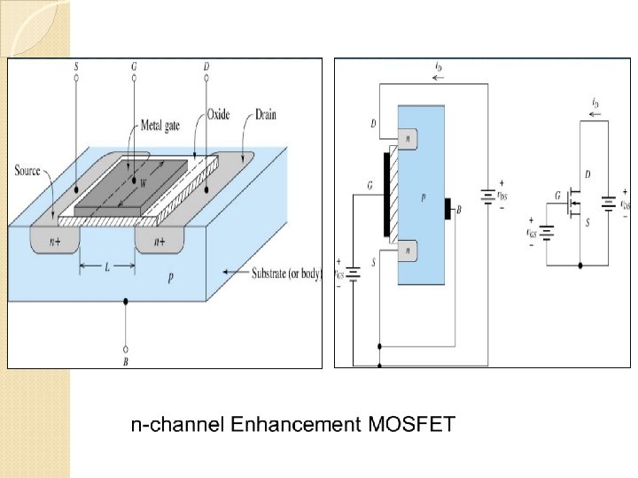
Enhancement-mode N-Channel MOSFET and Circuit Symboles enhancement mode mosfet symbol Enhancement-mode MOSFETs make excellent electronics switches due to their low “ON” resistance and extremely high “OFF” resistance as well as their infinitely high input resistance due to their isolated gate. Enhancementmode MOSFETs are used in integrated circuits to produce CMOS type Logic Gates and power switching circuits in the form of as PMOS (P-channel) and NMOS (N-channel) gates. CMOS actually stands for Complementary MOS meaning that the logic device has both PMOS and NMOS within its design.
Non-saturation(Ohmic)Region VDS < (VGS – VP) The drain current is given by IDS=2 IDSS/V²P [ (VGS-VP)VDS-V²DS/2) ] Saturation(or pinchoff)Region VDS ≥ ( VGS – VP ) IDS=IDSS/V²P [ (VGS – VP)² ] AND IDS=IDSS ( 1 – VGS / VP )²
VOLTAGE AND CURRENT CHARACTERISTICS FOR MOSFET Depletion-Type MOSFET Enhancement-Type MOSFET
The transistor is composed of galactic effect from: 1. Substrate, which is either N type or P. 2. . Two regions of two crystals of the same type opposite the bottom layer N <==> P and represent two ends of the transistor, namely Drain and Source 3. A layer of oxide (SIO 2), a non-conductive material (dielectric) 4. . A layer of metal represents the third party of the transistor gate. . Also, the transistor has two types: P-Channel and NChannel, depending on the type of the bottom layer and the two side crystals (the bank and the source).
MOSFET Business Idea: In this type of transistors the current is controlled by the voltage (electric field) inside. So how? See the following figure (where the bank is connected to the positive terminal of the battery and the source to its negative terminal). 1. If no voltage is placed on the Gate gate, no current will pass between the upstream and the bank (left). 2. If a positive voltage is placed on the gate (in the right shape), note that the transistor is of the channel type N, the free electrons in the source and bank crystals will be attracted to the positive electric field formed at the gate to form a channel for the current between the source and the bank. The size of this channel varies depending on the strength of the electric field at the gate and thus changes the value of the current flowing between the source and the bank.
3. If a negative voltage is placed on the gate (in the right shape), note that the transistor is of the type P channel, the gaps in the source and bank crystals will be attracted to the negative electric field formed at the gate to form a channel for the current between the source and the bank. The size of this channel varies depending on the strength of the electric field at the gate and thus changes the value of the current flowing between the source and the bank. Note that because of the insulating oxide between the gate and the rest of the transistor, the current does not pass between them and only the current flowing between the source and the bank is controlled by the voltage (electric field) on the gate .
Special Types: Dual-Gate MOSFET The two-gate MOSFET is a special design for the transistor. The label also has two links to the gate, so that the steering current can enter its gates respectively (in sequence) and be independent of each other. This means that the efficiency or connection capacity between the bank and the source can be changed. This type is used in the radio. . : (Vertical Metal-Oxide-Semiconductor) VMOSFET (FET) is suitable for relatively low capacity due to the relatively long distance in the channel (approximately 5 micrometers), where penetration resistance is from 1 k ohm to 10 k ohm The current capabilities of the manufacturing technology allow for greater effort and flow. By constructing a vertical layer in addition to the horizontal layers, the current reaches 10 amperes and the voltage between the bank (D) and the source (S) reaches 100 volts.
(Vertical Metal-Oxide-Semiconductor Siemens Power) SIPMOS-FET It is similar to the VMOS-FET installation according to the fact that its flat-panel technology is of any type. Its penetration resistance ranges up to about m ohm and is often used as a fast power switch. Output characteristics curve of connector type and channel type N:
MESFETs Use of Ga As in the construction of semiconductor devices. The need For high-Speed devices and improved Production methods in recent years Have been established astrong demand for Large-scale integrated circuits using Ga As
Basic Construction of an n-channel MESFETs
Schottky barriers are barriers established by depositing a metal such as on n-type channel. The absence of an insulating layer reduces the distanceinbetween theofmetal contact resulting a lower level stray capacitance surface Between of the two surfaces wich reduced sensetivity to the highgate frequencies , semiconductor layer and the with further Supports the high mobility of carriers in the GA AS material. The presence of metal-semiconductor junction Is the reason such FETs are called “metalsemiconductor field-effect transistors (MESFETs)
Depletion-type MESFET are so similar to � those of the applied to depletion-type MOSFETs. There also enhancement-type MESFETs with aconstruction of symbol The response and are essentially the same as for the enhancement-type MOSFET Depletion –type and enhancement –type MESFETs are made with an n-channel between the drain and the source and therefore only n-type MESFETs are commercially available.
The general relationships that can be applied to the dc of analysis of all FET amplifiers are IG =~0 A------------(2 -8) ID=IS For JFETs and depletion –type MOSFETs and MESFETs Shockley’s equation is applied ID=Idss(1 -VGs/VP)^2 For enhancement MOSFETs and MESFETs , the following equation is applicable ID=K (VGs-VT)^2