Recent Development of Fin FET Technology for CMOS
![Corner Effect [1] Vg=0. 2 V D Vg=1 V z z y y G Corner Effect [1] Vg=0. 2 V D Vg=1 V z z y y G](https://slidetodoc.com/presentation_image/3312d36bf09abf0c269fde80f34ce0ec/image-30.jpg)
![Corner Effect [2] n Nsub=5 e 18 cm-3 z corner y Vg=0. 2 V Corner Effect [2] n Nsub=5 e 18 cm-3 z corner y Vg=0. 2 V](https://slidetodoc.com/presentation_image/3312d36bf09abf0c269fde80f34ce0ec/image-31.jpg)
![Volume Inversion [1] Gate T si N sub =10 Gate e. Density 6. 1 Volume Inversion [1] Gate T si N sub =10 Gate e. Density 6. 1](https://slidetodoc.com/presentation_image/3312d36bf09abf0c269fde80f34ce0ec/image-35.jpg)
![Volume Inversion [2] q For intrinsic channel doping, volume inversion is valid and the Volume Inversion [2] q For intrinsic channel doping, volume inversion is valid and the](https://slidetodoc.com/presentation_image/3312d36bf09abf0c269fde80f34ce0ec/image-36.jpg)
- Slides: 71

Recent Development of Fin. FET Technology for CMOS Logic and Memory Chung-Hsun Lin EECS Department University of California at Berkeley

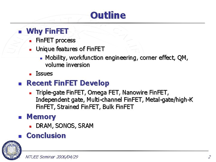
Outline n Why Fin. FET n n Recent Fin. FET Develop n n Triple-gate Fin. FET, Omega FET, Nanowire Fin. FET, Independent gate, Multi-channel Fin. FET, Metal-gate/high-K Fin. FET, Strained Fin. FET, Bulk Fin. FET Memory n n Fin. FET process Unique features of Fin. FET n Mobility, workfunction engineering, corne r effect, QM, volume inversion Issues DRAM, SONOS, SRAM Conclusion NTUEE Seminar 2006/04/29 2

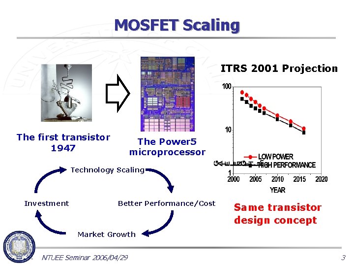
MOSFET Scaling ITRS 2001 Projection The first transistor 1947 The Power 5 microprocessor Technology Scaling Investment Better Performance/Cost Same transistor design concept Market Growth NTUEE Seminar 2006/04/29 3

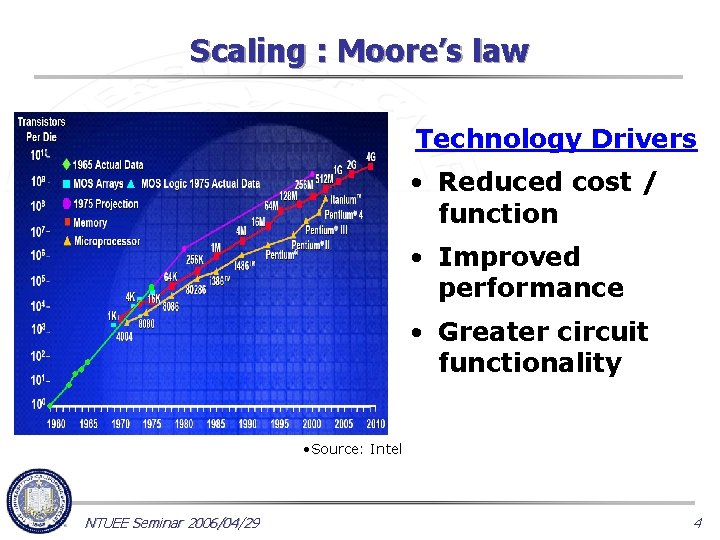
Scaling : Moore’s law Technology Drivers • Reduced cost / function • Improved performance • Greater circuit functionality • Source: Intel NTUEE Seminar 2006/04/29 4

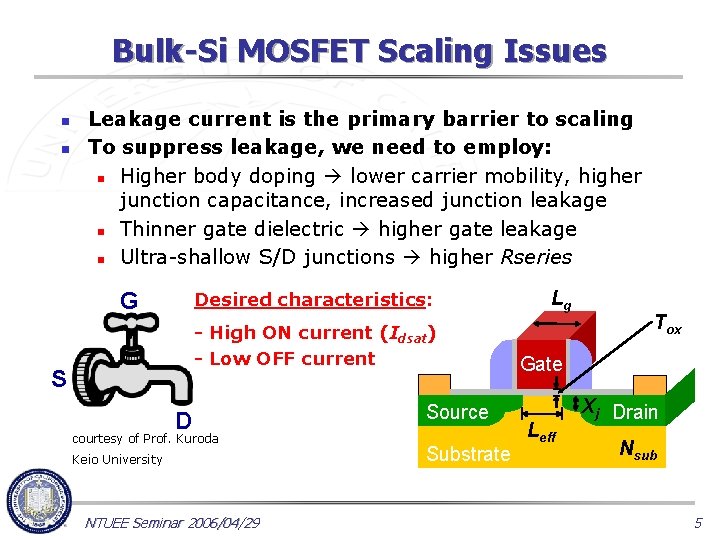
Bulk-Si MOSFET Scaling Issues n n Leakage current is the primary barrier to scaling To suppress leakage, we need to employ: n Higher body doping lower carrier mobility, higher junction capacitance, increased junction leakage n Thinner gate dielectric higher gate leakage n Ultra-shallow S/D junctions higher Rseries G Desired characteristics: - High ON current (Idsat) - Low OFF current S D courtesy of Prof. Kuroda Keio University NTUEE Seminar 2006/04/29 Source Substrate Lg Tox Gate Leff Xj Drain Nsub 5

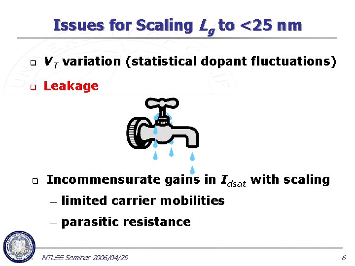
Issues for Scaling Lg to <25 nm q VT variation (statistical dopant fluctuations) q Leakage q Incommensurate gains in Idsat with scaling — limited carrier mobilities — parasitic resistance NTUEE Seminar 2006/04/29 6

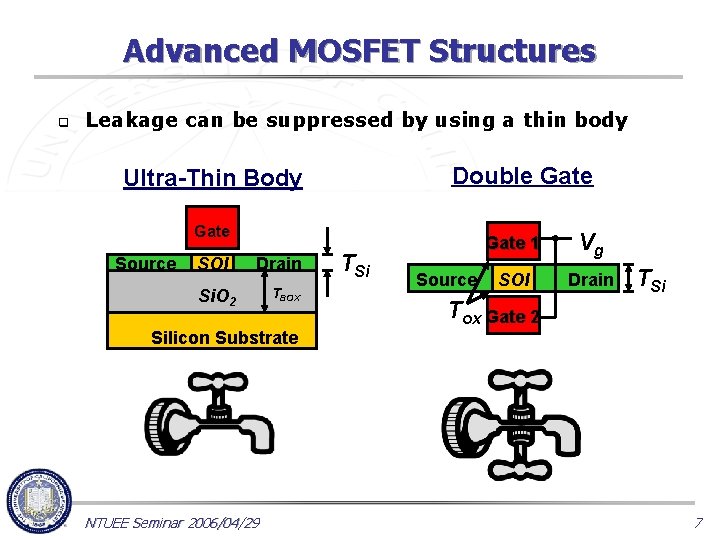
Advanced MOSFET Structures q Leakage can be suppressed by using a thin body Double Gate Ultra-Thin Body Gate Source SOI Drain Si. O 2 TBOX Silicon Substrate NTUEE Seminar 2006/04/29 TSi Source Gate 1 Vg SOI Drain TSi Tox Gate 2 7

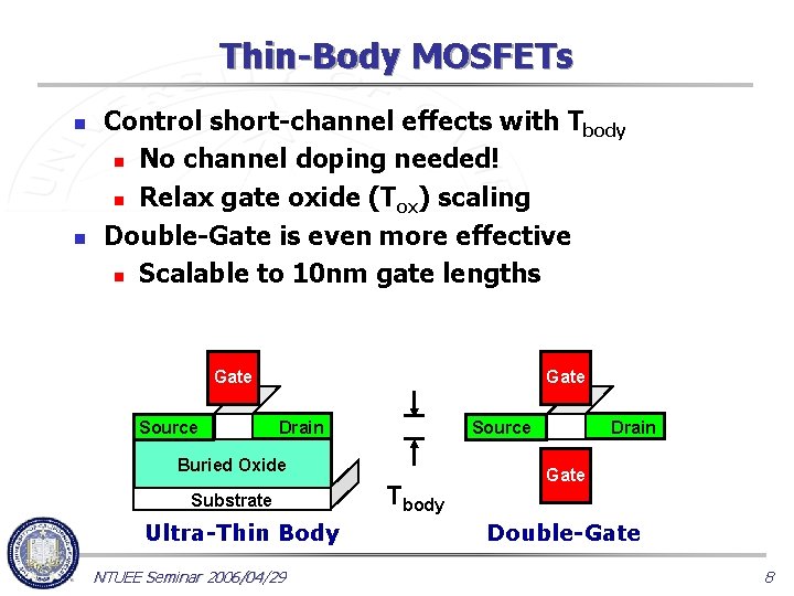
Thin-Body MOSFETs n n Control short-channel effects with Tbody n No channel doping needed! n Relax gate oxide (Tox) scaling Double-Gate is even more effective n Scalable to 10 nm gate lengths Gate Source Gate Drain Source Buried Oxide Substrate Ultra-Thin Body NTUEE Seminar 2006/04/29 Tbody Drain Gate Double-Gate 8

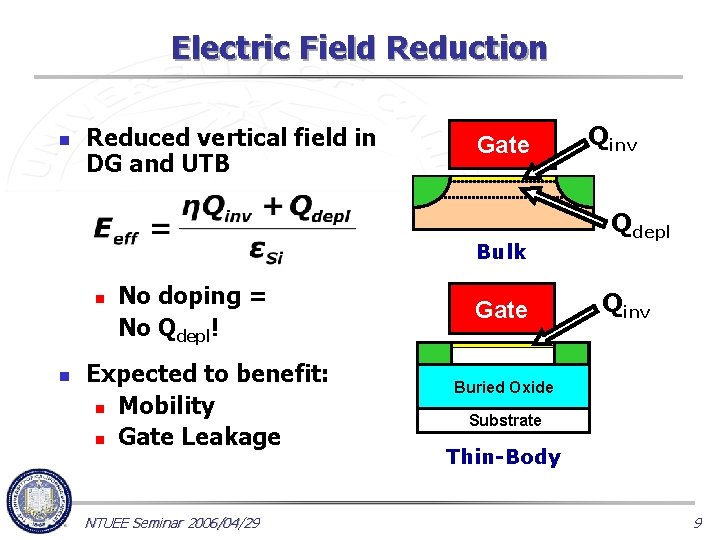
Electric Field Reduction n Reduced vertical field in DG and UTB Gate Bulk n n No doping = No Qdepl! Expected to benefit: n Mobility n Gate Leakage NTUEE Seminar 2006/04/29 Gate Qinv Qdepl Qinv Buried Oxide Substrate Thin-Body 9

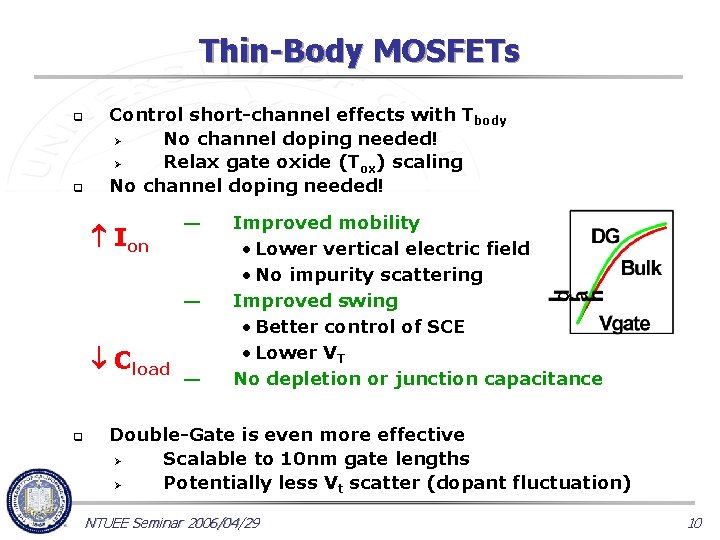
Thin-Body MOSFETs q q Control short-channel effects with Tbody Ø No channel doping needed! Ø Relax gate oxide (Tox) scaling No channel doping needed! Ion — — Cload q — Improved mobility • Lower vertical electric field • No impurity scattering Improved swing • Better control of SCE • Lower VT No depletion or junction capacitance Double-Gate is even more effective Ø Scalable to 10 nm gate lengths Ø Potentially less Vt scatter (dopant fluctuation) NTUEE Seminar 2006/04/29 10

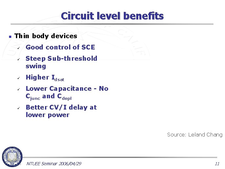
Circuit level benefits n Thin body devices ü ü ü Good control of SCE Steep Sub-threshold swing Tbody, UTB = 5 nm Higher Idsat Lower Capacitance - No Cjunc and Cdepl Better CV/I delay at lower power Tbody, UTB < 5 nm 50 35 25 18 Source: Leland Chang NTUEE Seminar 2006/04/29 11

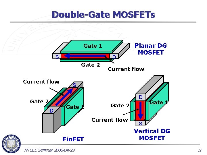
Double-Gate MOSFETs Gate 1 S D Gate 2 Current flow Planar DG MOSFET Current flow S D Gate 2 D Gate 1 Gate 2 Current flow Fin. FET NTUEE Seminar 2006/04/29 Gate 1 S Vertical DG MOSFET 12

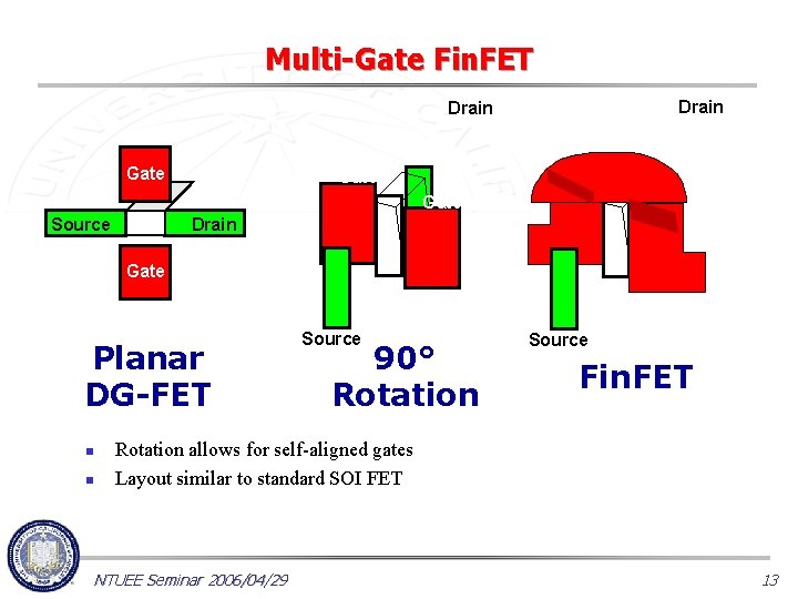
Multi-Gate Fin. FET Drain Gate Gate Source Drain Gate Planar DG-FET n n Source 90° Rotation Source Fin. FET Rotation allows for self-aligned gates Layout similar to standard SOI FET NTUEE Seminar 2006/04/29 13

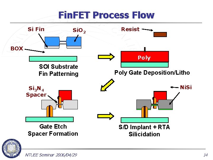
Fin. FET Process Flow Si Fin Si. O 2 Resist BOX Poly SOI Substrate Fin Patterning Poly Gate Deposition/Litho Ni. Si Si 3 N 4 Spacer Gate Etch Spacer Formation NTUEE Seminar 2006/04/29 S/D Implant + RTA Silicidation 14

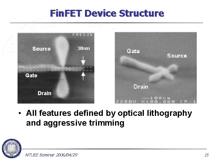
Fin. FET Device Structure Source Gate Drain • All features defined by optical lithography and aggressive trimming NTUEE Seminar 2006/04/29 15

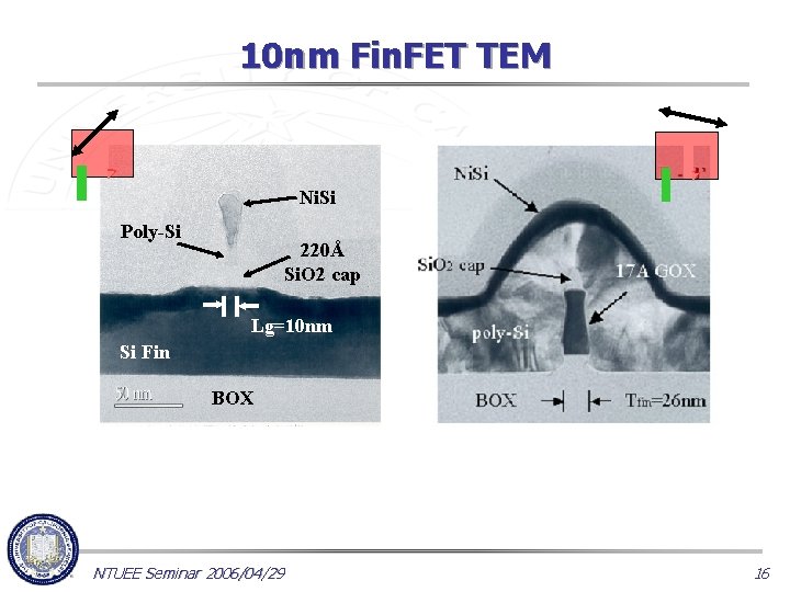
10 nm Fin. FET TEM Ni. Si Poly-Si 220Å Si. O 2 cap Lg=10 nm Si Fin BOX NTUEE Seminar 2006/04/29 16

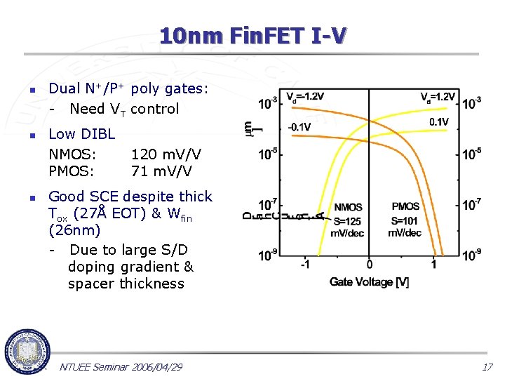
10 nm Fin. FET I-V n n n Dual N+/P+ poly gates: - Need VT control Low DIBL NMOS: PMOS: 120 m. V/V 71 m. V/V Good SCE despite thick Tox (27Å EOT) & Wfin (26 nm) - Due to large S/D doping gradient & spacer thickness NTUEE Seminar 2006/04/29 17

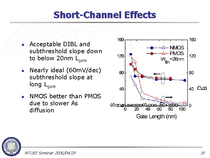
Short-Channel Effects n n n Acceptable DIBL and subthreshold slope down to below 20 nm Lgate Nearly ideal (60 m. V/dec) subthreshold slope at long Lgate NMOS better than PMOS due to slower As diffusion NTUEE Seminar 2006/04/29 18

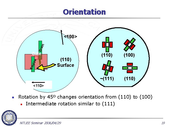
Orientation Dra in <100> So urc e Gate (110) Surface (110) (100) ~(111) (110) <110> n Rotation by 45º changes orientation from (110) to (100) n Intermediate rotation similar to (111) NTUEE Seminar 2006/04/29 19

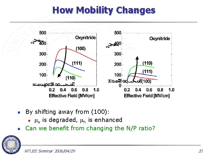
How Mobility Changes n n By shifting away from (100): n e is degraded, h is enhanced Can we benefit from changing the N/P ratio? NTUEE Seminar 2006/04/29 20

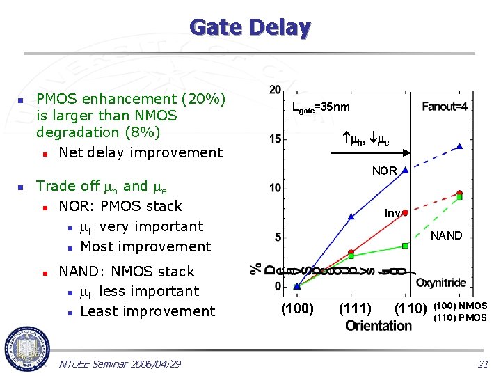
Gate Delay n n PMOS enhancement (20%) is larger than NMOS degradation (8%) n Net delay improvement Lgate=35 nm h, e NOR Trade off h and e n NOR: PMOS stack n h very important n Most improvement n NAND: NMOS stack n h less important n Least improvement NTUEE Seminar 2006/04/29 Inv NAND (100) (111) (110) (100) NMOS (110) PMOS 21

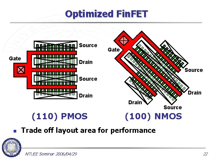
Optimized Fin. FET Source Gate Drain Source Drain (110) PMOS n Source (100) NMOS Trade off layout area for performance NTUEE Seminar 2006/04/29 22

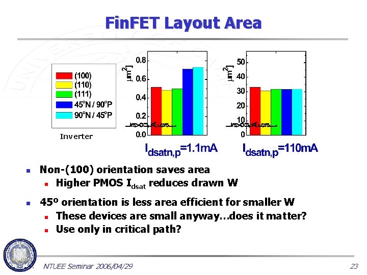
Fin. FET Layout Area Inverter n n Non-(100) orientation saves area n Higher PMOS Idsat reduces drawn W 45º orientation is less area efficient for smaller W n These devices are small anyway…does it matter? n Use only in critical path? NTUEE Seminar 2006/04/29 23

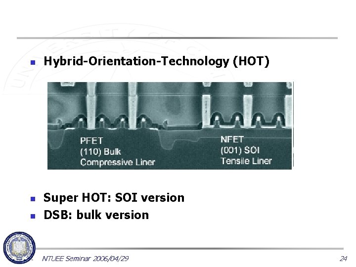
n n n Hybrid-Orientation-Technology (HOT) Super HOT: SOI version DSB: bulk version NTUEE Seminar 2006/04/29 24

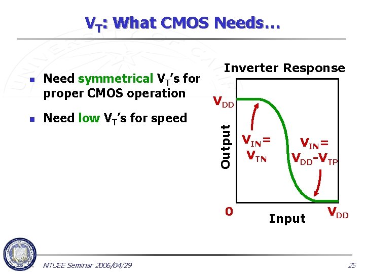
VT: What CMOS Needs… n Need symmetrical VT’s for proper CMOS operation Need low VT’s for speed VDD Output n Inverter Response 0 NTUEE Seminar 2006/04/29 VIN= VTN VIN= VDD-VTP Input VDD 25

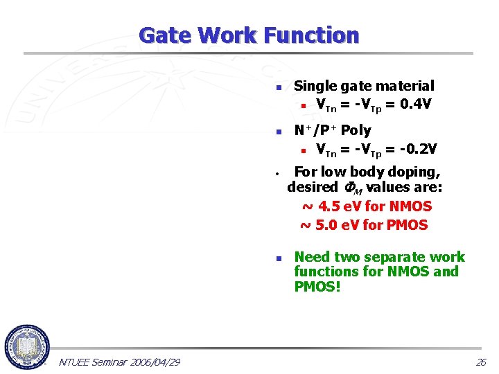
Gate Work Function n n • n NTUEE Seminar 2006/04/29 Single gate material n VTn = -VTp = 0. 4 V N+/P+ Poly n VTn = -VTp = -0. 2 V For low body doping, desired FM values are: ~ 4. 5 e. V for NMOS ~ 5. 0 e. V for PMOS Need two separate work functions for NMOS and PMOS! 26

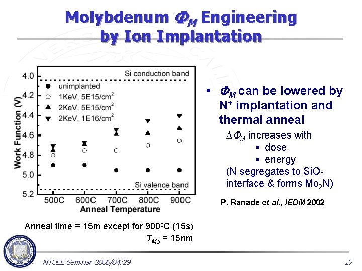
Molybdenum FM Engineering by Ion Implantation § FM can be lowered by N+ implantation and thermal anneal DFM increases with § dose § energy (N segregates to Si. O 2 interface & forms Mo 2 N) P. Ranade et al. , IEDM 2002 Anneal time = 15 m except for 900 o. C (15 s) TMo = 15 nm NTUEE Seminar 2006/04/29 27

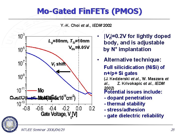
Mo-Gated Fin. FETs (PMOS) Y. -K. Choi et al. , IEDM 2002 Lg=80 nm, TSi=10 nm Vds=0. 05 V Vt shift • |Vt|=0. 2 V for lightly doped body, and is adjustable by N+ implantation • Alternative technique: Full silicidication (Ni. Si) of n+/p+ Si gates (J. Kedzierski et al. , W. Maszara et al. , Z. Krivokapic et al. , IEDM 2002) Potential issues include: - dopant penetration - thermal stability - stress/adhesion - gate dielectric reliability NTUEE Seminar 2006/04/29 28

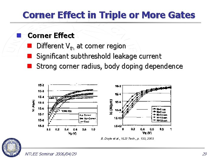
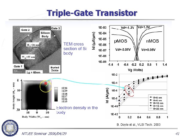
Corner Effect in Triple or More Gates n Corner Effect n Different Vth at corner region n Significant subthreshold leakage current n Strong corner radius, body doping dependence B. Doyle et al. , VLSI Tech. , p. 133, 2003 NTUEE Seminar 2006/04/29 29
![Corner Effect 1 Vg0 2 V D Vg1 V z z y y G Corner Effect [1] Vg=0. 2 V D Vg=1 V z z y y G](https://slidetodoc.com/presentation_image/3312d36bf09abf0c269fde80f34ce0ec/image-30.jpg)
Corner Effect [1] Vg=0. 2 V D Vg=1 V z z y y G S 2 D current density distribution n 2 D current density distribution DESSIS 3 -D device simulator Ideal rectangular fin shape Nsub=1 e 15 cm-3 NTUEE Seminar 2006/04/29 30
![Corner Effect 2 n Nsub5 e 18 cm3 z corner y Vg0 2 V Corner Effect [2] n Nsub=5 e 18 cm-3 z corner y Vg=0. 2 V](https://slidetodoc.com/presentation_image/3312d36bf09abf0c269fde80f34ce0ec/image-31.jpg)
Corner Effect [2] n Nsub=5 e 18 cm-3 z corner y Vg=0. 2 V flat 2 D current density distribution z y Vg=1 V 2 D current density distribution NTUEE Seminar 2006/04/29 31

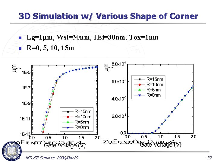
3 D Simulation w/ Various Shape of Corner n n Lg=1 m, Wsi=30 nm, Hsi=30 nm, Tox=1 nm R=0, 5, 10, 15 m NTUEE Seminar 2006/04/29 32

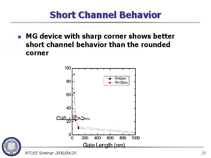
Short Channel Behavior n MG device with sharp corner shows better short channel behavior than the rounded corner NTUEE Seminar 2006/04/29 33

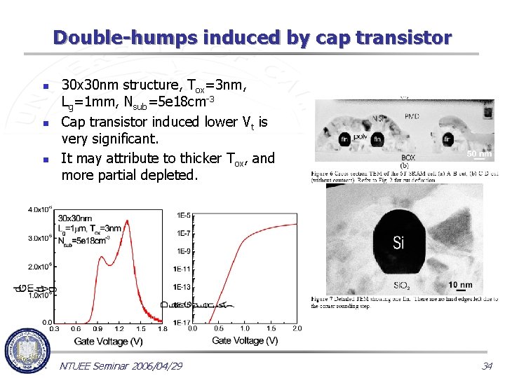
Double-humps induced by cap transistor n n n 30 x 30 nm structure, Tox=3 nm, Lg=1 mm, Nsub=5 e 18 cm-3 Cap transistor induced lower Vt is very significant. It may attribute to thicker Tox, and more partial depleted. NTUEE Seminar 2006/04/29 34
![Volume Inversion 1 Gate T si N sub 10 Gate e Density 6 1 Volume Inversion [1] Gate T si N sub =10 Gate e. Density 6. 1](https://slidetodoc.com/presentation_image/3312d36bf09abf0c269fde80f34ce0ec/image-35.jpg)
Volume Inversion [1] Gate T si N sub =10 Gate e. Density 6. 1 E+13 5. 3 E+13 T si 4. 5 E+13 15 cm Oxide -3 4. 5 E+13 3. 6 E+13 2. 8 E+13 2. 0 E+13 N sub =10 18 cm -3 Oxide The electron density distribution from the 3 -D ISE device simulator. Volume inversion is significant in intrinsic channel SDG (left). NTUEE Seminar 2006/04/29 35
![Volume Inversion 2 q For intrinsic channel doping volume inversion is valid and the Volume Inversion [2] q For intrinsic channel doping, volume inversion is valid and the](https://slidetodoc.com/presentation_image/3312d36bf09abf0c269fde80f34ce0ec/image-36.jpg)
Volume Inversion [2] q For intrinsic channel doping, volume inversion is valid and the potential through the Si film is flat in the subthreshold region. q The inversion charge (current) in the subthreshold region is proportional to Tsi. NTUEE Seminar 2006/04/29 36

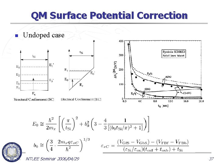
QM Surface Potential Correction n Undoped case NTUEE Seminar 2006/04/29 37

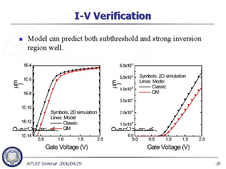
I-V Verification n Model can predict both subthreshold and strong inversion region well. NTUEE Seminar 2006/04/29 38

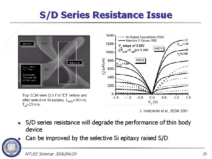
S/D Series Resistance Issue J. Kedzierski et al. , IEDM 2001 n n S/D series resistance will degrade the performance of thin body device Can be improved by the selective Si epitaxy raised S/D NTUEE Seminar 2006/04/29 39

Outline n Why Fin. FET n n Recent Fin. FET Develop n n Triple-gate Fin. FET, Omega FET, Nanowire Fin. FET, Independent gate, Multi-channel Fin. FET, Metal-gate/high-K Fin. FET, Strained Fin. FET, Bulk Fin. FET Memory n n Fin. FET process Unique features of Fin. FET n Mobility, workfunction engineering, corne r effect, QM, volume inversion Issues DRAM, SONOS, SRAM Conclusion NTUEE Seminar 2006/04/29 40

Triple-Gate Transistor B. Doyle et al. , VLSI Tech. 2003 NTUEE Seminar 2006/04/29 41

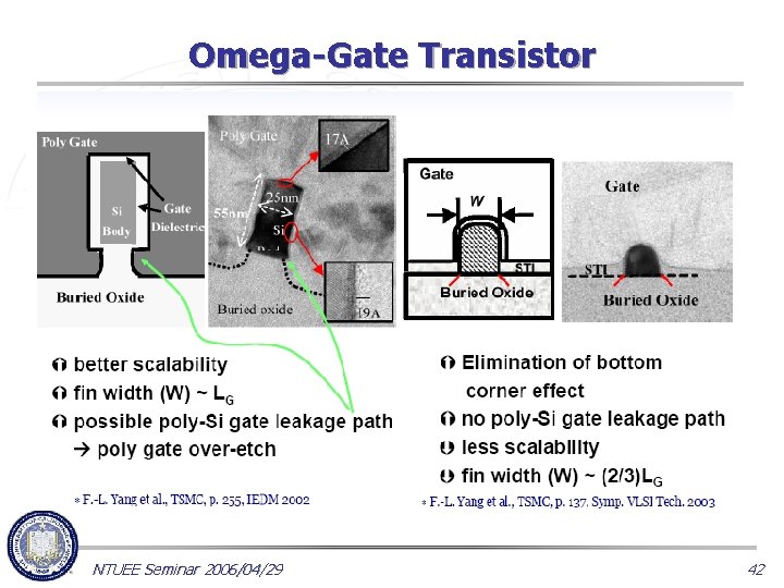
Omega-Gate Transistor NTUEE Seminar 2006/04/29 42

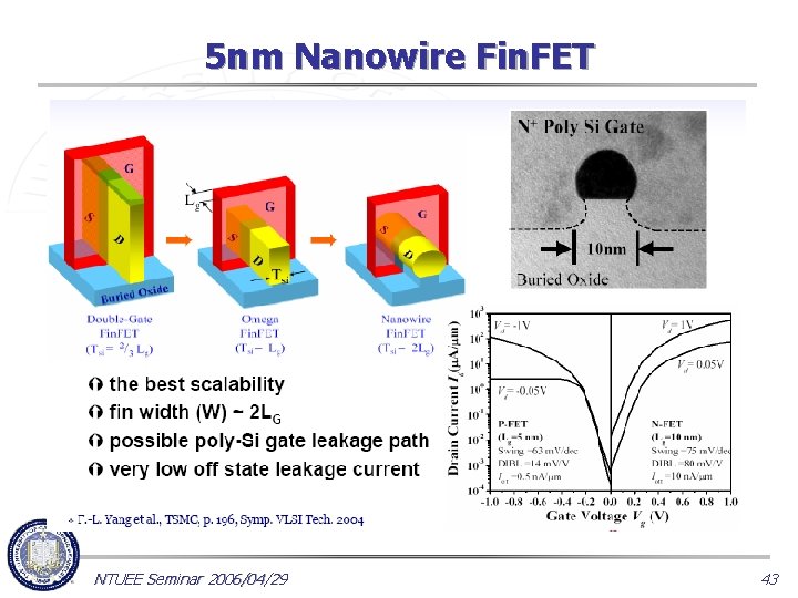
5 nm Nanowire Fin. FET NTUEE Seminar 2006/04/29 43

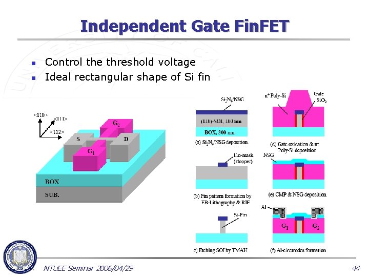
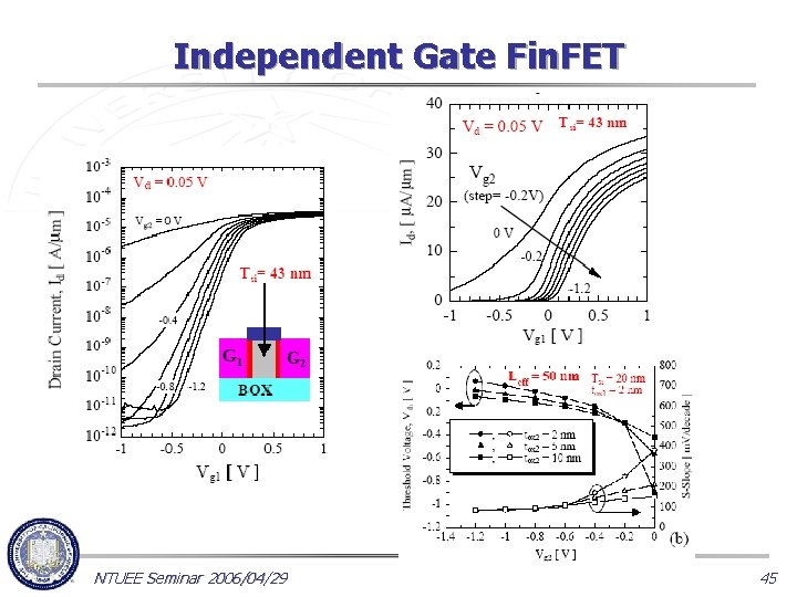
Independent Gate Fin. FET n n Control the threshold voltage Ideal rectangular shape of Si fin NTUEE Seminar 2006/04/29 44

Independent Gate Fin. FET NTUEE Seminar 2006/04/29 45

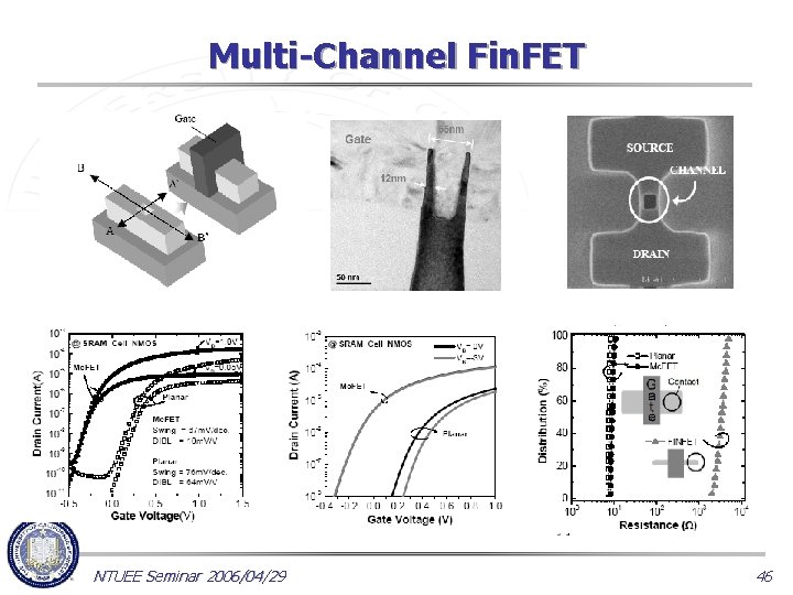
Multi-Channel Fin. FET NTUEE Seminar 2006/04/29 46

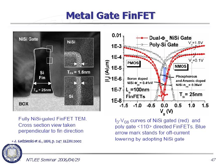
Metal Gate Fin. FET NTUEE Seminar 2006/04/29 47

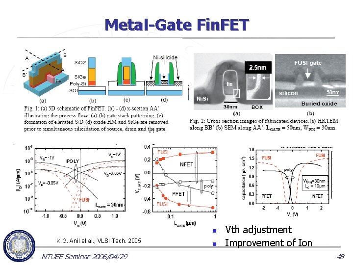
Metal-Gate Fin. FET n K. G. Anil et al. , VLSI Tech. 2005 NTUEE Seminar 2006/04/29 n Vth adjustment Improvement of Ion 48

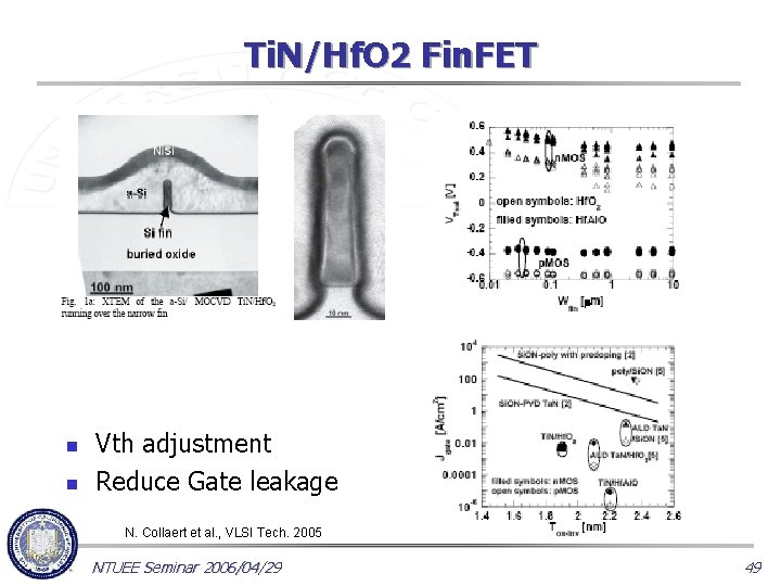
Ti. N/Hf. O 2 Fin. FET n n Vth adjustment Reduce Gate leakage N. Collaert et al. , VLSI Tech. 2005 NTUEE Seminar 2006/04/29 49

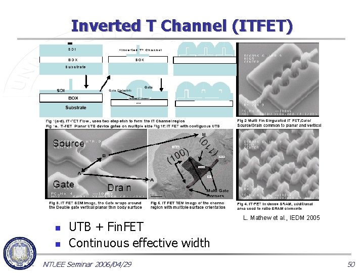
Inverted T Channel (ITFET) n n UTB + Fin. FET Continuous effective width NTUEE Seminar 2006/04/29 L. Mathew et al. , IEDM 2005 50

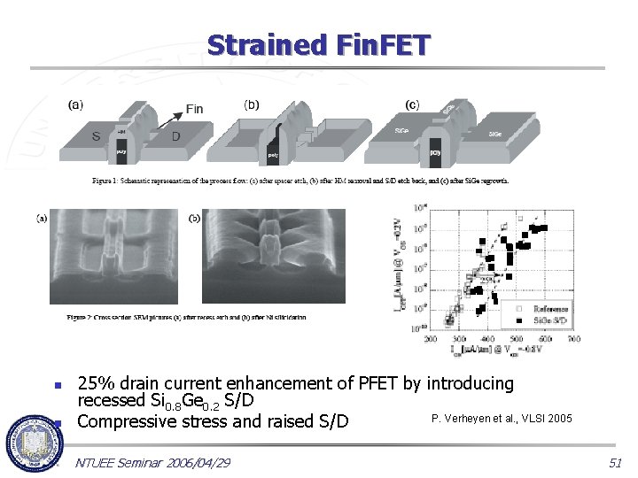
Strained Fin. FET n n 25% drain current enhancement of PFET by introducing recessed Si 0. 8 Ge 0. 2 S/D P. Verheyen et al. , VLSI 2005 Compressive stress and raised S/D NTUEE Seminar 2006/04/29 51

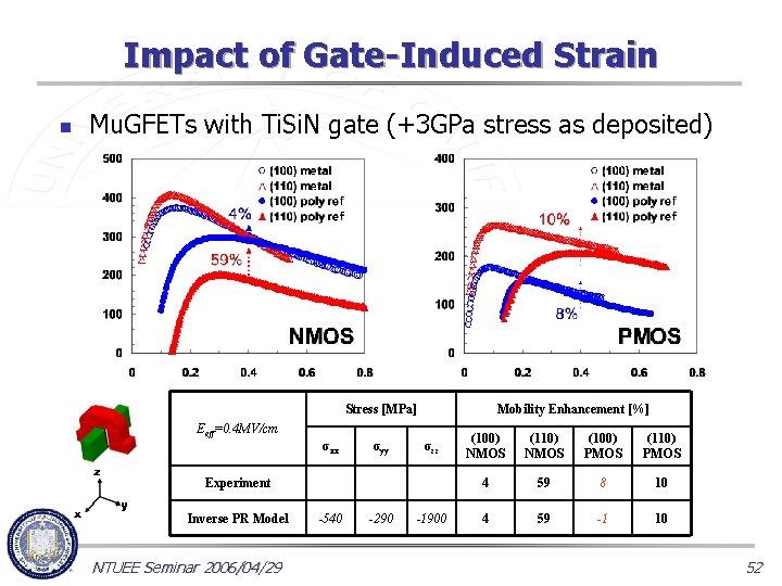
Impact of Gate-Induced Strain n Mu. GFETs with Ti. Si. N gate (+3 GPa stress as deposited) Stress [MPa] Mobility Enhancement [%] Eeff=0. 4 MV/cm σxx σyy σzz Experiment Inverse PR Model NTUEE Seminar 2006/04/29 -540 -290 -1900 (100) NMOS (110) NMOS (100) PMOS (110) PMOS 4 59 8 10 4 59 -1 10 52

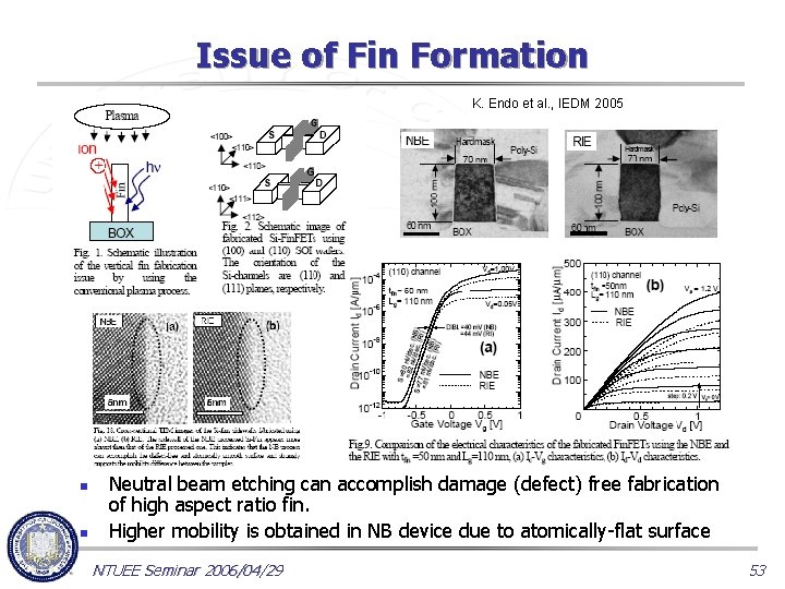
Issue of Fin Formation K. Endo et al. , IEDM 2005 n n Neutral beam etching can accomplish damage (defect) free fabrication of high aspect ratio fin. Higher mobility is obtained in NB device due to atomically-flat surface NTUEE Seminar 2006/04/29 53

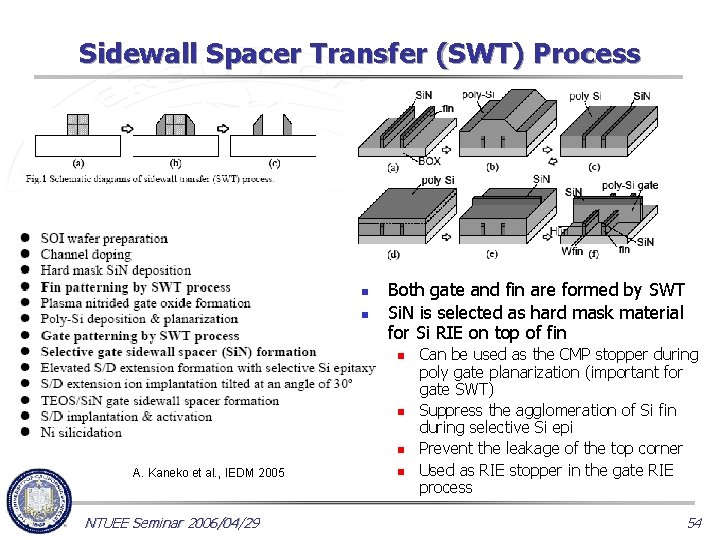
Sidewall Spacer Transfer (SWT) Process n n Both gate and fin are formed by SWT Si. N is selected as hard mask material for Si RIE on top of fin n A. Kaneko et al. , IEDM 2005 NTUEE Seminar 2006/04/29 n Can be used as the CMP stopper during poly gate planarization (important for gate SWT) Suppress the agglomeration of Si fin during selective Si epi Prevent the leakage of the top corner Used as RIE stopper in the gate RIE process 54

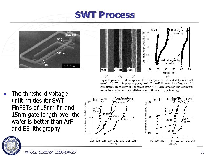
SWT Process n The threshold voltage uniformities for SWT Fin. FETs of 15 nm fin and 15 nm gate length over the wafer is better than Ar. F and EB lithography NTUEE Seminar 2006/04/29 55

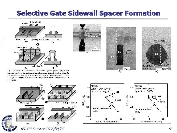
Selective Gate Sidewall Spacer Formation NTUEE Seminar 2006/04/29 56

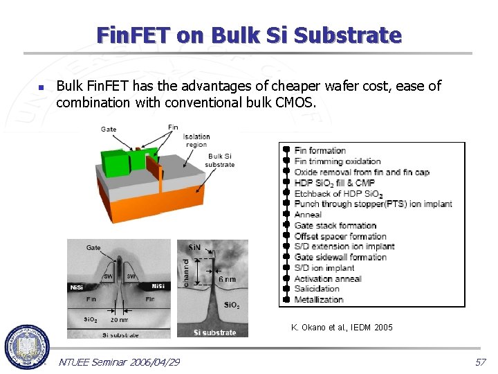
Fin. FET on Bulk Si Substrate n Bulk Fin. FET has the advantages of cheaper wafer cost, ease of combination with conventional bulk CMOS. K. Okano et al. , IEDM 2005 NTUEE Seminar 2006/04/29 57

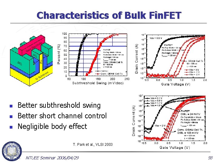
Characteristics of Bulk Fin. FET n n n Better subthreshold swing Better short channel control Negligible body effect T. Park et al. , VLSI 2003 NTUEE Seminar 2006/04/29 58

Outline n Why Fin. FET n n Recent Fin. FET Develop n n Triple-gate Fin. FET, Omega FET, Nanowire Fin. FET, Independent gate, Multi-channel Fin. FET, Metal-gate/high-K Fin. FET, Strained Fin. FET, Bulk Fin. FET Memory n n Fin. FET process Unique features of Fin. FET n Mobility, workfunction engineering, corne r effect, QM, volume inversion Issues DRAM, SONOS, SRAM Conclusion NTUEE Seminar 2006/04/29 59

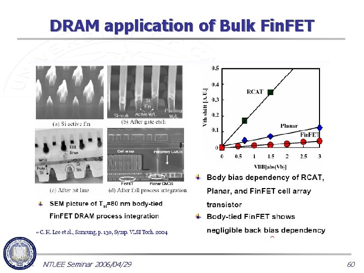
DRAM application of Bulk Fin. FET NTUEE Seminar 2006/04/29 60

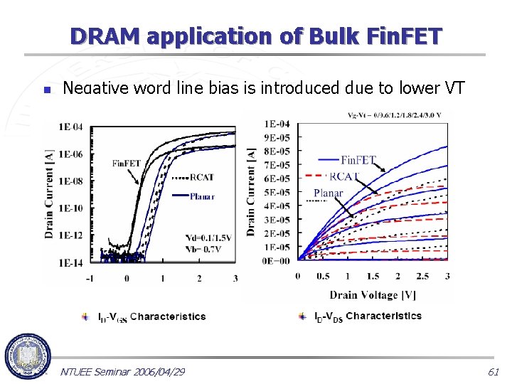
DRAM application of Bulk Fin. FET n Negative word line bias is introduced due to lower VT NTUEE Seminar 2006/04/29 61

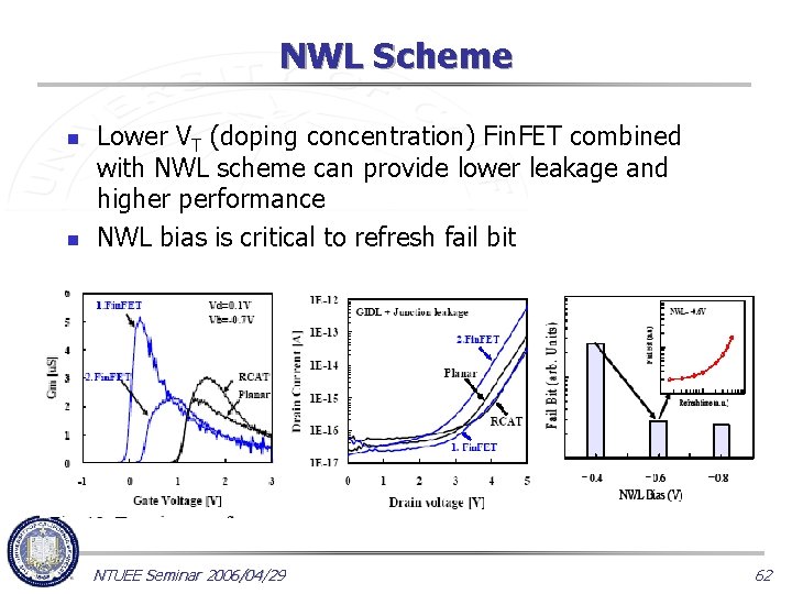
NWL Scheme n n Lower VT (doping concentration) Fin. FET combined with NWL scheme can provide lower leakage and higher performance NWL bias is critical to refresh fail bit NTUEE Seminar 2006/04/29 62

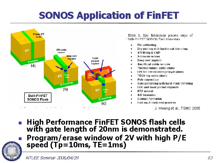
SONOS Application of Fin. FET J. Hwang et al. , TSMC 2005 n n High Performance Fin. FET SONOS flash cells with gate length of 20 nm is demonstrated. Program/erase window of 2 V with high P/E speed (Tp=10 ms, TE=1 ms) NTUEE Seminar 2006/04/29 63

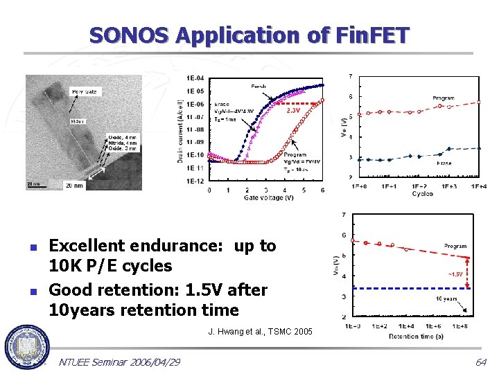
SONOS Application of Fin. FET n n Excellent endurance: up to 10 K P/E cycles Good retention: 1. 5 V after 10 years retention time J. Hwang et al. , TSMC 2005 NTUEE Seminar 2006/04/29 64

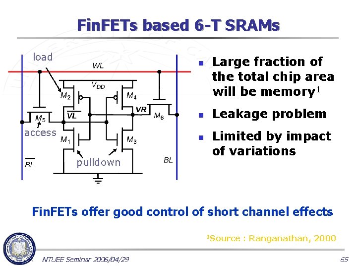
Fin. FETs based 6 -T SRAMs load n n access n pulldown Large fraction of the total chip area will be memory 1 Leakage problem Limited by impact of variations Fin. FETs offer good control of short channel effects 1 Source NTUEE Seminar 2006/04/29 : Ranganathan, 2000 65

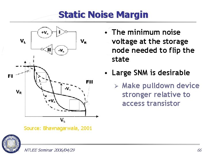
Static Noise Margin • The minimum noise voltage at the storage node needed to flip the state • Large SNM is desirable Ø Make pulldown device stronger relative to access transistor Source: Bhavnagarwala, 2001 NTUEE Seminar 2006/04/29 66

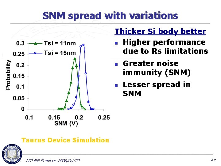
SNM spread with variations Thicker Si body better n Higher performance due to Rs limitations n n Greater noise immunity (SNM) Lesser spread in SNM Taurus Device Simulation NTUEE Seminar 2006/04/29 67

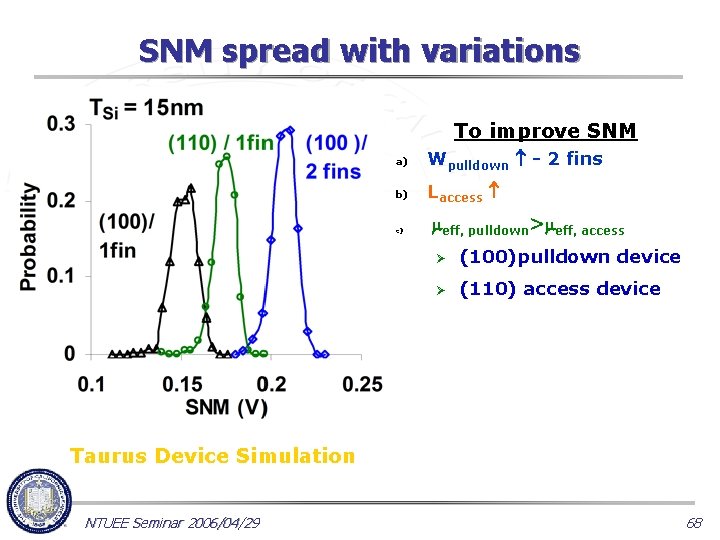
SNM spread with variations To improve SNM a) Wpulldown - 2 fins b) Laccess c) eff, pulldown> eff, access Ø (100)pulldown device Ø (110) access device Taurus Device Simulation NTUEE Seminar 2006/04/29 68

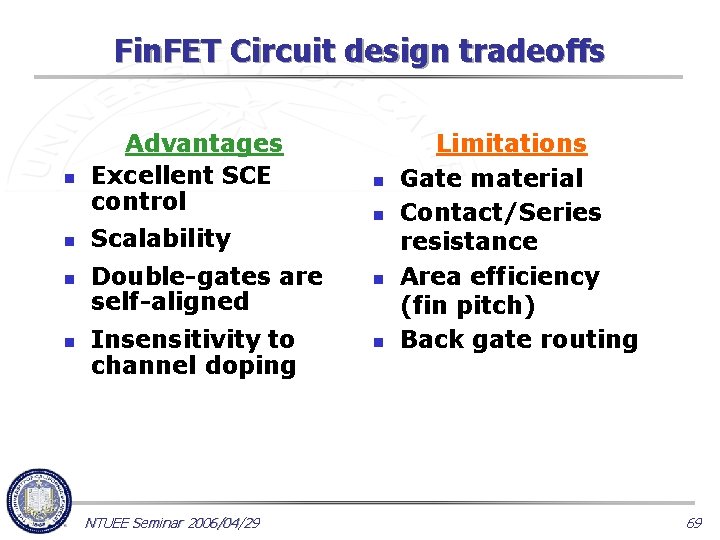
Fin. FET Circuit design tradeoffs n n Advantages Excellent SCE control Scalability Double-gates are self-aligned Insensitivity to channel doping NTUEE Seminar 2006/04/29 n n Limitations Gate material Contact/Series resistance Area efficiency (fin pitch) Back gate routing 69

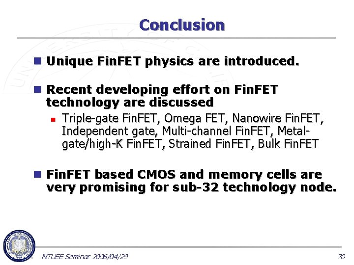
Conclusion n Unique Fin. FET physics are introduced. n Recent developing effort on Fin. FET technology are discussed n Triple-gate Fin. FET, Omega FET, Nanowire Fin. FET, Independent gate, Multi-channel Fin. FET, Metalgate/high-K Fin. FET, Strained Fin. FET, Bulk Fin. FET n Fin. FET based CMOS and memory cells are very promising for sub-32 technology node. NTUEE Seminar 2006/04/29 70

Thank you very much for your attention NTUEE Seminar 2006/04/29 71