Introduction to the bipolar junction transistor Bipolar Action

Introduction to the bipolar junction transistor

Bipolar Action ?

In this lecture, you will learn • • • the structure of the BJT the band diagram of the BJT the principle of operation of the BJT Read : 1. Neamen, “Semiconductor Physics and Devices”, 3 rd Edition, (2003), pp. 367 -370. 2. Muller, Kamins and Chan, “Device Electronics for Integrated Circuits”, 3 rd Edition, (2003), pp. 278 -279.

• The microelectronics revolution – started with the invention of the bipolar junction transistor (bjt) in 1947 by Brattain, Bardeen and Shockley of Bell Laboratories. • Bipolar transistors – main devices in electronics in the 1950 s to early 1960 s, – superseded by the MOSFET in most integrated circuits today, – still an important device in applications where high current drive or very high speed is essential. – making a comeback in Bi. CMOS devices
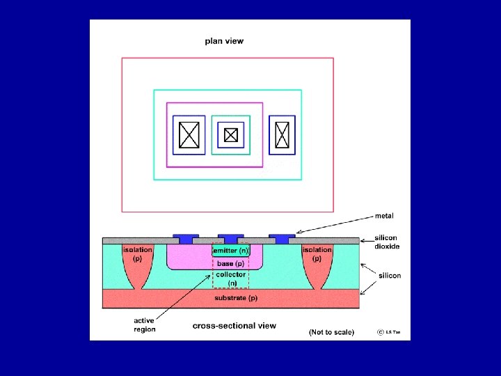

• Structure of an n-p-n bipolar transistor : – – – Heavily doped n-type emitter, Less heavily doped p-type base, Moderately / lightly n-type doped collector, May also have a heavily doped sub-collector, Nested within one another. • In ICs, the transistor are isolated from one another by isolation regions, e. g. reverse-biased p-n junctions.
, (relative to what ? )")
• Base of bipolar transistor – Short (narrow), (relative to what ? ) – Interactions can take place between the two p-n junctions. • Operation of bipolar transistor – Depends on both majority and minority carriers – Hence the name “bipolar”.

Bipolar Transistor in equilibrium • At the E-B junction, electron flow E→B = B→E. Similarly for hole flow. • Same situation at C-B junction. • Hence, no net current flows through the transistor.

Bipolar transistor in in forward active mode – The emitter-base junction is forward biased. – The collector-base junction is reverse biased. bjt simulation and animation applet. html

At the emitter-base junction : – energy barrier is reduced, – net diffusion of electrons from emitter into base, – net diffusion of holes from base into emitter. Emitter doping >> base doping, – Most of the carrier that cross the junctions are electrons that diffuse from emitter into base (n-p-n transistor) Example : If emitter doping = 99 X base doping, then out of 100 carriers that cross the junction, 99 are electrons and 1 is a hole.
,")
In the neutral base region : – injected electrons are minority carriers (n-p-n transistor), – they diffuse across the neutral base towards the collector-base junction, – very few of the electrons recombine with holes in the neutral base, because the base is very short compared to the minority carrier diffusion length, – practically all the electrons injected from the emitter into the base reach the collector-base junction.

At the collector-base junction : – Normally, the current that flows through a reversebiased p-n junction is very small. – In this case, there is a large supply of electrons (minority carriers) that originate from the emitter. – The electric field at the collector-base junction sweeps the electrons into the collector to form the collector current.

There is a small base current. – supply holes to replace those that are injected from the base into the emitter, – supply holes that recombine with electrons n the neutral base.

• The forward bias at the emitter-base junction can be considered from two (equivalent) viewpoints. First, the bias can be considered as a voltage applied between the base and the emitter, as a result of which a current flows through the emitter-base junction, as the energy barrier across the junction is reduced. • Equivalently, this bias can be considered as the application of a current to the base terminal. As holes are supplied to the base, some of them are forced across the emitter-based junction from the base into the emitter, and in the process, forward biasing the junction.

• Because of the unequal doping between the emitter and the base, for every hole that is injected from the base into the emitter, a large number (e. g. , say 99) electrons will go from the emitter into the base. Almost all of these electrons will survive the diffusion across the base into the collector, to give rise to the collector current. • Therefore, the application of a small current at the base terminal can result in a large current at the collector terminal. There is therefore an amplification effect.

• Question : • If the application of a small current at the base of the bipolar transistor results in a large current at the collector, wouldn’t this violate the principle of conservation of energy ?

bjt simulation and animation applet. html • When both the E-B and C-B junctions are forward biased : • Electrons (for an n-p-n transistor) are injected from both the emitter and the collector into the base. • The base is saturated with electrons, and the voltage across the emitter and collector is very low (typically about 0. 2 V). • The bipolar transistor then behaves like a short circuit.

• When both the emitter-base junction and the collector-base junctions are reverse biased : • Only small leakage currents flow through the junctions. • The transistor effectively behaves like an open circuit. • The short circuit and open circuit states of the bipolar transistor can be used in circuits to denote the “ 1” and “ 0” states of a binary system.
- Slides: 18