Timing process Instruction It is a command which


 Opcode fetch m/c")


- Slides: 37
Timing & process § Instruction: -It is a command which direct the processor to execute certain task. Ex: - MOV A, B I. Op-code: what operation the MP will perform. Ex: -MOV II. Operand: - On which data the MP will operated on. Ex: - A, B
Instruction cycle: - The time taken to complete the execution of one instruction. Machine Cycle: - The time taken to complete the execution of one machine. Each reference of the MP to its peripherals is one machine cycle.
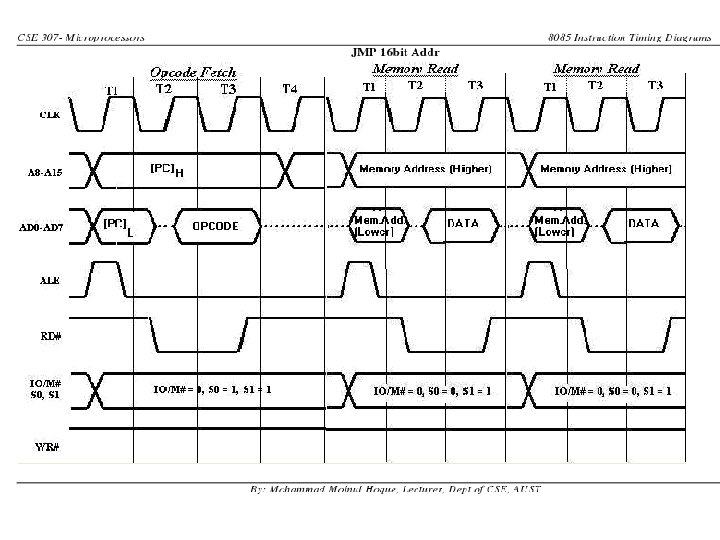
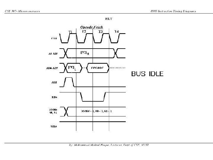
Types of Machine cycle • • Opcode fetch m/c (6 T) Opcode fetch m/c (4 T) Memory read m/c (3 T) Memory write m/c (3 T) I/O read m/c -3 T I/O write m/c -3 T Bus Idle m/c - Undefined
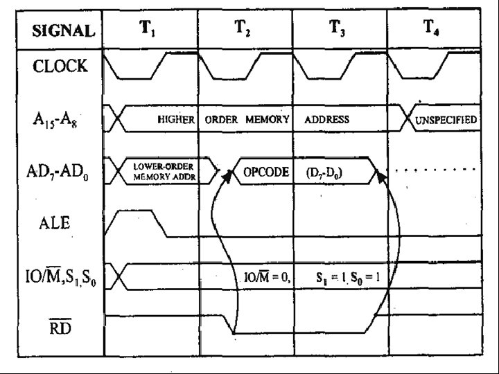
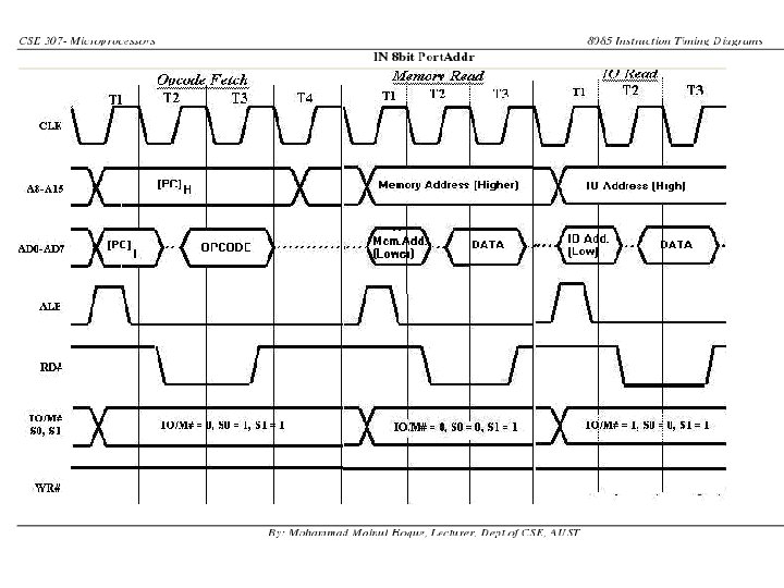
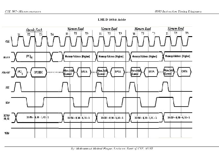
Opcode fetch machine cycle of 8085 : • Each instruction of the processor has one byte opcode. • The opcodes are stored in memory. So, the processor executes the opcode fetch machine cycle to fetch the opcode from memory. • Hence, every instruction starts with opcode fetch machine cycle. • The time taken by the processor to execute the opcode fetch cycle is 4 T. • In this time, the first, 3 T-states are used for fetching the opcode from memory and the remaining T-states are used for internal operations by the processor.
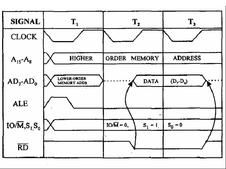
Memory Read Machine Cycle of 8085: • The memory read machine cycle is executed by the processor to read a data byte from memory. • The processor takes 3 T states to execute this cycle. • The instructions which have more than one byte word size will use the machine cycle after the opcode fetch machine cycle.
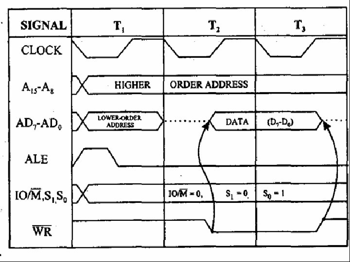
Memory Write Machine Cycle • The memory write machine cycle is executed by the processor to write a data byte in a memory location. • The processor takes, 3 T states to execute this machine cycle.
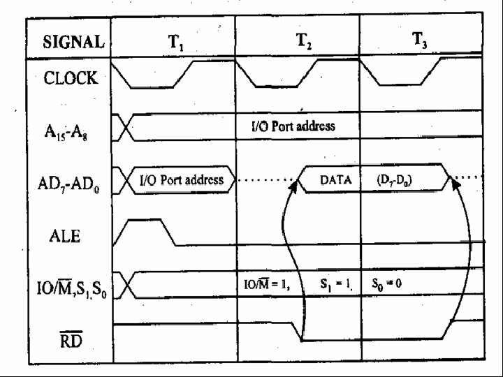
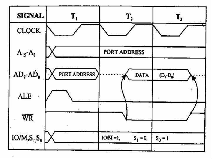
I/O Read Cycle of 8085: • The I/O Read cycle is executed by the processor to read a data byte from I/O port or from the peripheral, which is I/O, mapped in the system. • The processor takes 3 T states to execute this machine cycle. • The IN instruction uses this machine cycle during the execution.
I/O Write Cycle of 8085: • The I/O write machine cycle is executed by the processor to write a data byte in the I/O port or to a peripheral, which is I/O, mapped in the system. • The processor takes, 3 T states to execute this machine cycle. •
Bus Idle machine cycle
Timing diagram for INR M • Fetching the Opcode 34 H from the memory 4105 H. (OF cycle) • Let the memory address (M) be 4250 H. (MR cycle -To read Memory address and data) • Let the content of that memory is 12 H. • Increment the memory content from 12 H to 13 H. (MW machine cycle)
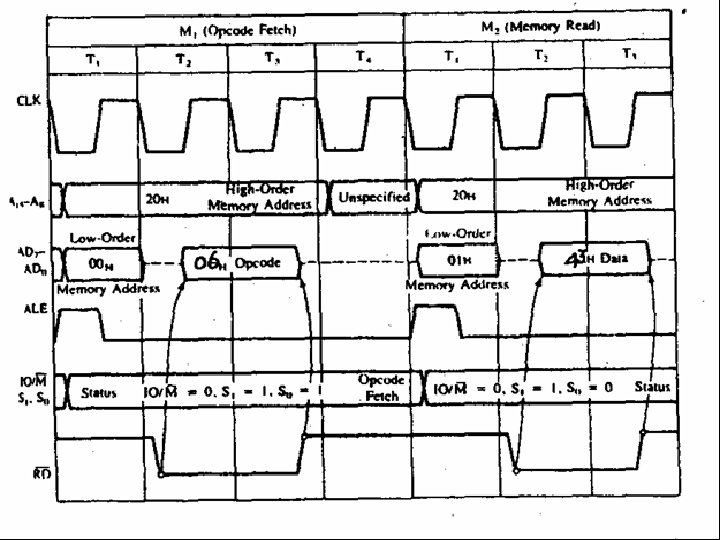
Timing diagram for MVI B, 43 H • Fetching the Opcode 06 H from the memory 2000 H. (OF machine cycle) • Read (move) the data 43 H from memory 2001 H. (memory read)
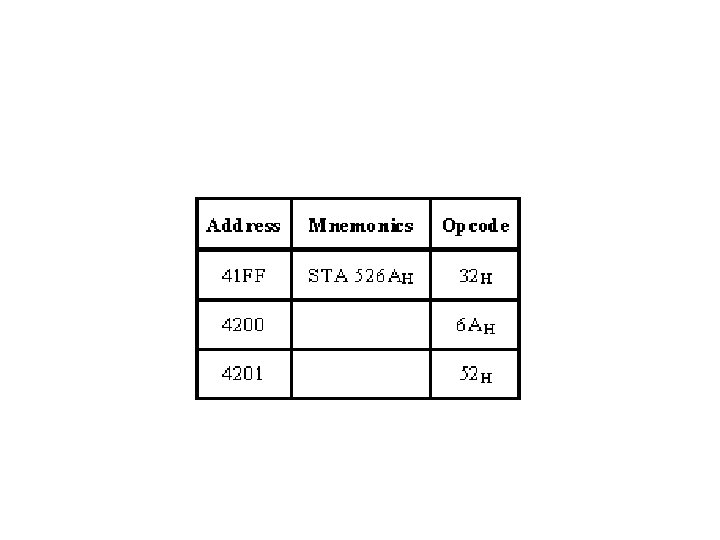
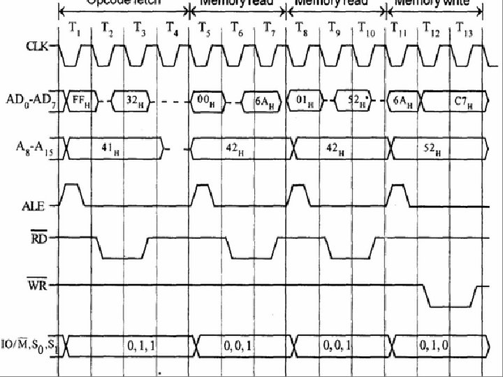
Timing diagram for STA 526 AH • STA means Store Accumulator -The contents of the accumulator is stored in the specified address(526 A). • The opcode of the STA instruction is said to be 32 H. It is fetched from the memory 41 FFH(see fig). - OF machine cycle • Then the lower order memory address is read(6 A). - Memory Read Machine Cycle • Read the higher order memory address (52). - Memory Read Machine Cycle • The combination of both the addresses are considered and the content from accumulator is written in 526 A. - Memory Write Machine Cycle • Assume the memory address for the instruction and let the content of accumulator is C 7 H. So, C 7 H from accumulator is now stored in 526 A.
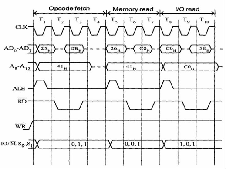
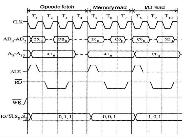
Timing diagram for IN C 0 H. • Fetching the Opcode DBH from the memory 4125 H. • Read the port address C 0 H from 4126 H. • Read the content of port C 0 H and send it to the accumulator. • Let the content of port is 5 EH.
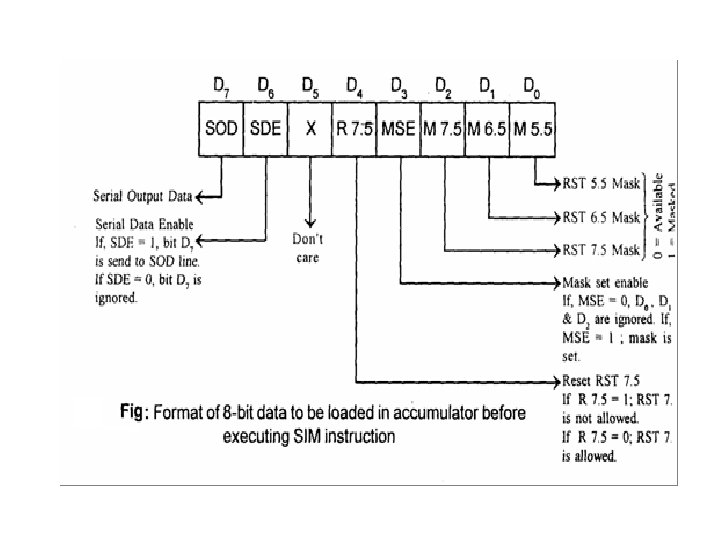
SIM and RIM for interrupts: • The 8085 provide additional masking facility for RST 7. 5, RST 6. 5 and RST 5. 5 using SIM instruction. • • The status of these interrupts can be read by executing RIM instruction. • • The masking or unmasking of RST 7. 5, RST 6. 5 and RST 5. 5 interrupts can be performed by moving an 8 -bit data to accumulator and then executing SIM instruction. • • The format of the 8 -bit data is shown below.
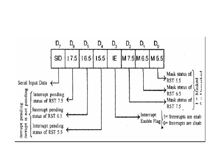
• The status of pending interrupts can be read from accumulator after executing RIM instruction. • • When RIM instruction is executed an 8 -bit data is loaded in accumulator, which can be interpreted as shown in fig.