The Demonstration of Dislocation Stress Memorization Technique DSMT
![SPEG: Stress Dependence v[001] v[110] Tensile Enhanced Retarded Compressive Slightly Retarded Slightly Enhanced Rudawski SPEG: Stress Dependence v[001] v[110] Tensile Enhanced Retarded Compressive Slightly Retarded Slightly Enhanced Rudawski](https://slidetodoc.com/presentation_image_h/ad9c6529ed53215fd97c2f904f7a78ca/image-24.jpg)

- Slides: 38

The Demonstration of Dislocation Stress Memorization Technique (D-SMT) on Si n. FET Student: Kun-Han, Liu Advisor: Ming-Han, Liao National Taiwan University 2014. 07. 21 Symposia on VLSI Technology and Circuits

Outline • • • Introduction Theoretical Background Demonstration of D-SMT on Silicon n. FET Solid-Phase Epitaxial Growth (SPEG) of Germanium Conclusions and Future Works Slide 1

Outline • • • Introduction Theoretical Background Demonstration of D-SMT on Silicon n. FET Solid-Phase Epitaxial Growth (SPEG) of Germanium Conclusions and Future Works Slide 2

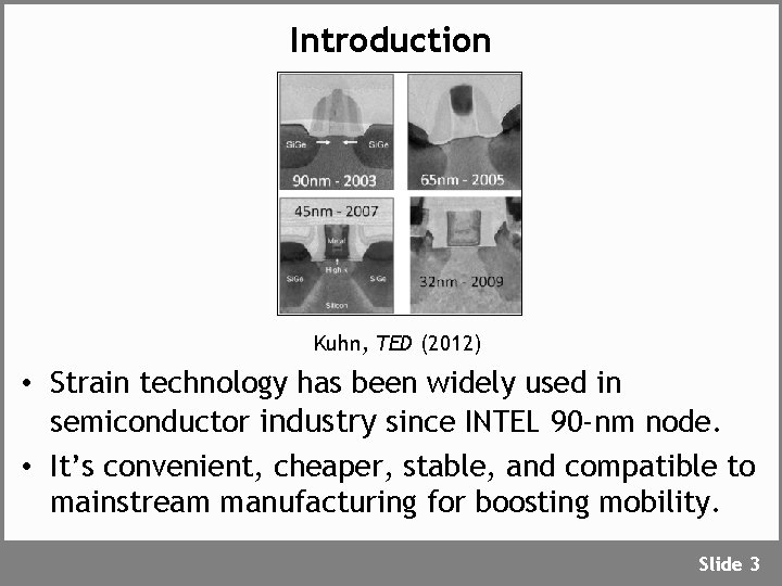
Introduction Kuhn, TED (2012) • Strain technology has been widely used in semiconductor industry since INTEL 90 -nm node. • It’s convenient, cheaper, stable, and compatible to mainstream manufacturing for boosting mobility. Slide 3

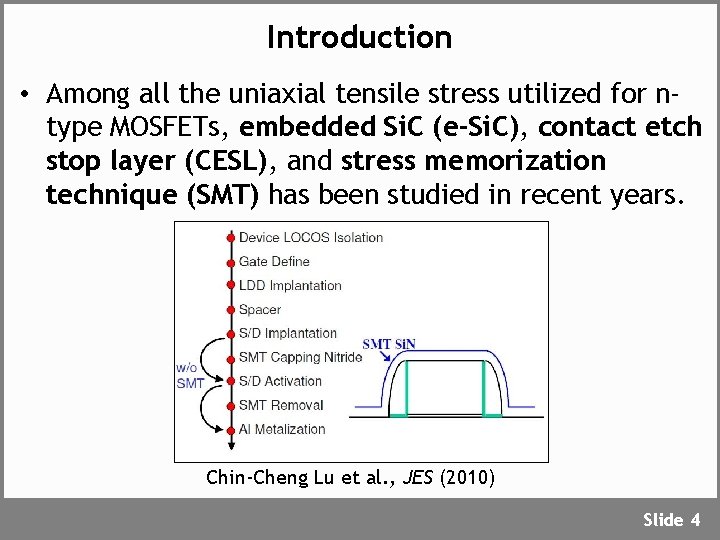
Introduction • Among all the uniaxial tensile stress utilized for ntype MOSFETs, embedded Si. C (e-Si. C), contact etch stop layer (CESL), and stress memorization technique (SMT) has been studied in recent years. Chin-Cheng Lu et al. , JES (2010) Slide 4

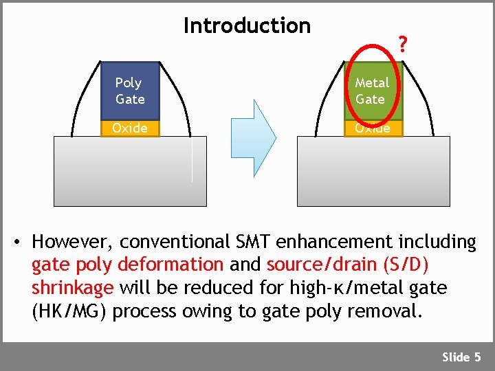
Introduction ? Poly Gate Metal Gate Oxide • However, conventional SMT enhancement including gate poly deformation and source/drain (S/D) shrinkage will be reduced for high-κ/metal gate (HK/MG) process owing to gate poly removal. Slide 5

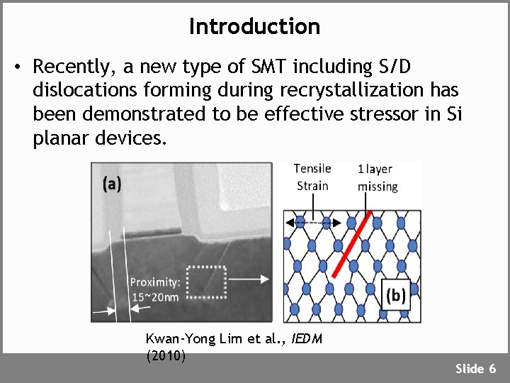
Introduction • Recently, a new type of SMT including S/D dislocations forming during recrystallization has been demonstrated to be effective stressor in Si planar devices. Kwan-Yong Lim et al. , IEDM (2010) Slide 6

Introduction • This work will present: – D-SMT as a stressor for Si n. FET through gate-first process. – Extend theory to Ge. Slide 7

Outline • • • Introduction Theoretical Background Demonstration of D-SMT on Silicon n. FET Solid-Phase Epitaxial Growth (SPEG) of Germanium Conclusions and Future Works Slide 8

Outline • Introduction • Theoretical Background – D-SMT Mechanism – Various Dependence of solid-phase epitaxial growth (SPEG) • Demonstration of D-SMT on Silicon n. FET • Solid-Phase Epitaxial Growth (SPEG) of Germanium • Conclusions and Future Works Slide 9

Outline • Introduction • Theoretical Background – D-SMT Mechanism – Various Dependence of solid-phase epitaxial growth (SPEG) • Demonstration of D-SMT on Silicon n. FET • Solid-Phase Epitaxial Growth (SPEG) of Germanium • Conclusions and Future Works Slide 10

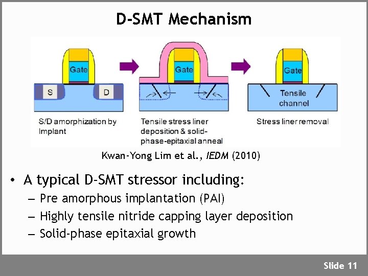
D-SMT Mechanism Kwan-Yong Lim et al. , IEDM (2010) • A typical D-SMT stressor including: – Pre amorphous implantation (PAI) – Highly tensile nitride capping layer deposition – Solid-phase epitaxial growth Slide 11

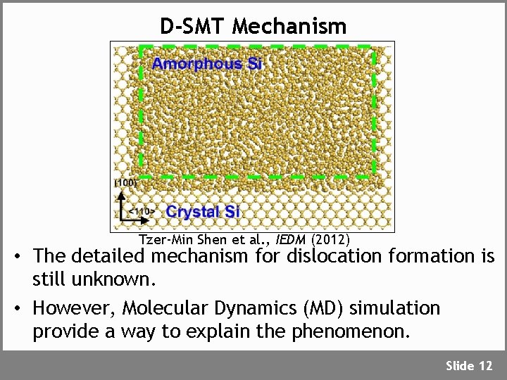
D-SMT Mechanism Tzer-Min Shen et al. , IEDM (2012) • The detailed mechanism for dislocation formation is still unknown. • However, Molecular Dynamics (MD) simulation provide a way to explain the phenomenon. Slide 12

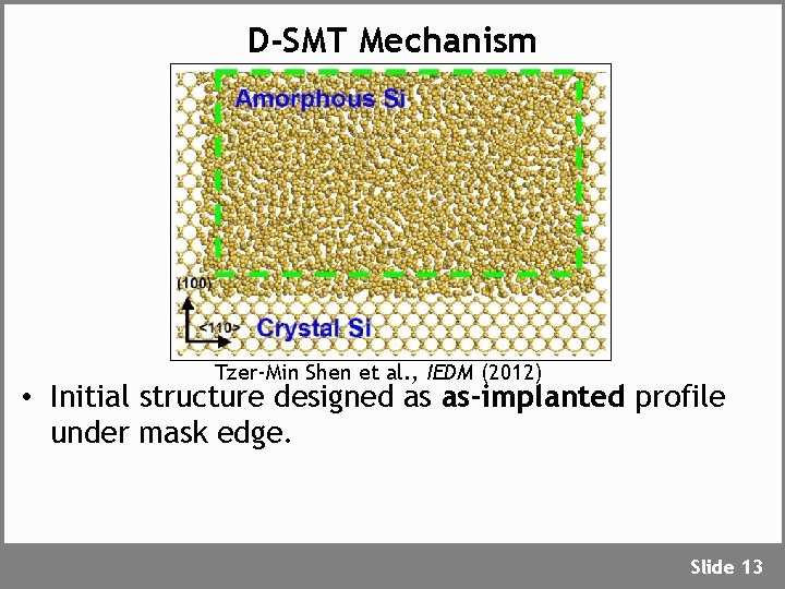
D-SMT Mechanism Tzer-Min Shen et al. , IEDM (2012) • Initial structure designed as as-implanted profile under mask edge. Slide 13

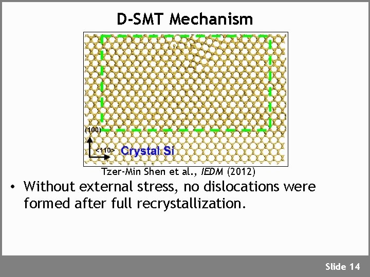
D-SMT Mechanism Tzer-Min Shen et al. , IEDM (2012) • Without external stress, no dislocations were formed after full recrystallization. Slide 14

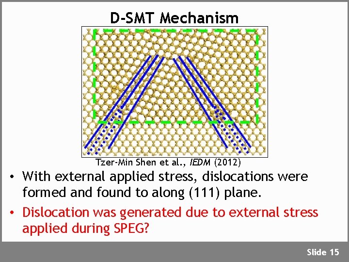
D-SMT Mechanism Tzer-Min Shen et al. , IEDM (2012) • With external applied stress, dislocations were formed and found to along (111) plane. • Dislocation was generated due to external stress applied during SPEG? Slide 15

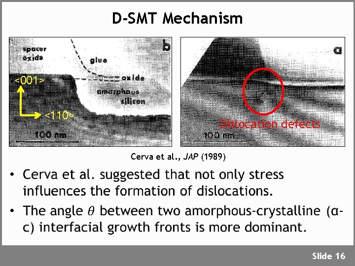
D-SMT Mechanism <<001> <<110> Dislocation defects Cerva et al. , JAP (1989) • Slide 16

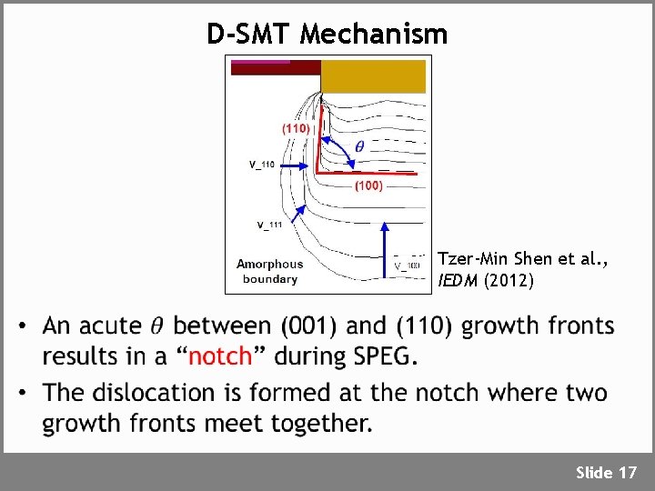
D-SMT Mechanism Tzer-Min Shen et al. , IEDM (2012) • Slide 17

Outline • Introduction • Theoretical Background – D-SMT Mechanism – Various Dependence of solid-phase epitaxial growth (SPEG) • Demonstration of D-SMT on Silicon n. FET • Solid-Phase Epitaxial Growth (SPEG) of Germanium • Conclusions and Future Works Slide 18

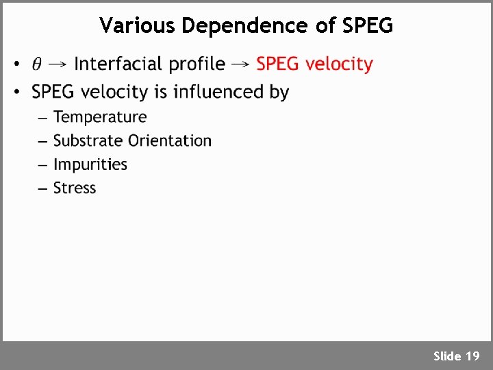
Various Dependence of SPEG • Slide 19

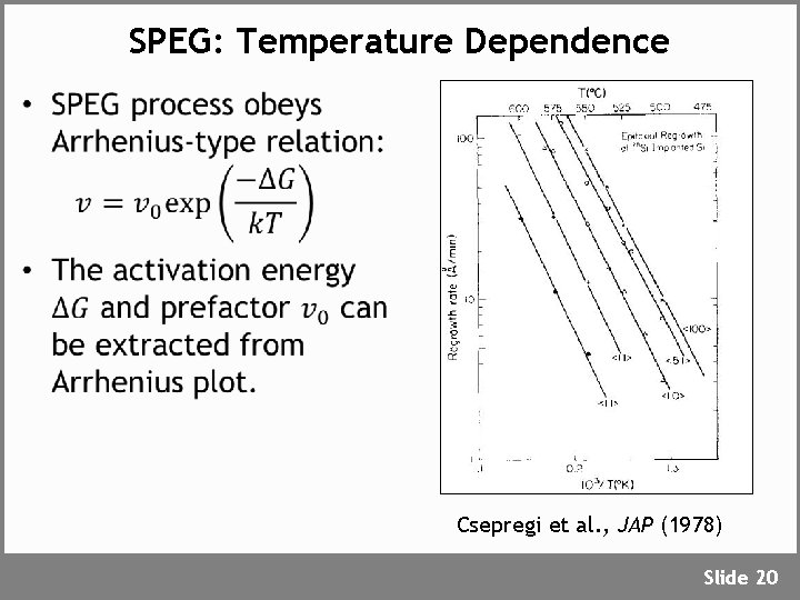
SPEG: Temperature Dependence • Csepregi et al. , JAP (1978) Slide 20

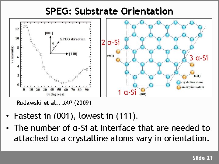
SPEG: Substrate Orientation 2 α-Si 3 α-Si 1 α-Si Rudawski et al. , JAP (2009) • Fastest in (001), lowest in (111). • The number of α-Si at interface that are needed to attached to a crystalline atoms vary in orientation. Slide 21

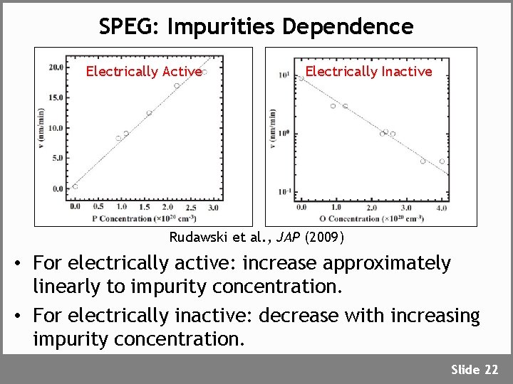
SPEG: Impurities Dependence Electrically Active Electrically Inactive Rudawski et al. , JAP (2009) • For electrically active: increase approximately linearly to impurity concentration. • For electrically inactive: decrease with increasing impurity concentration. Slide 22
![SPEG Stress Dependence v001 v110 Tensile Enhanced Retarded Compressive Slightly Retarded Slightly Enhanced Rudawski SPEG: Stress Dependence v[001] v[110] Tensile Enhanced Retarded Compressive Slightly Retarded Slightly Enhanced Rudawski](https://slidetodoc.com/presentation_image_h/ad9c6529ed53215fd97c2f904f7a78ca/image-24.jpg)
SPEG: Stress Dependence v[001] v[110] Tensile Enhanced Retarded Compressive Slightly Retarded Slightly Enhanced Rudawski et al. , JAP (2009) • SPEG velocity changes due to distance distortion causing by externally applied stress. • Depending on different substrate orientation. Slide 23

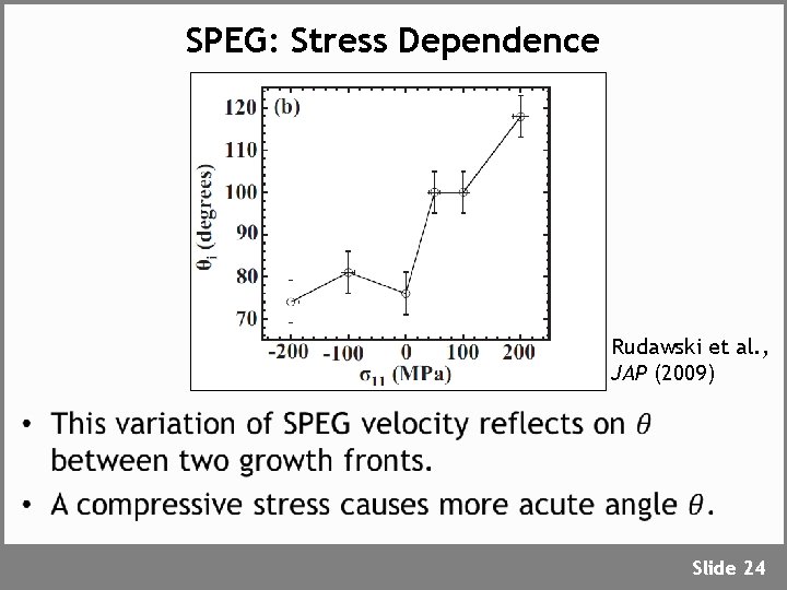
SPEG: Stress Dependence Rudawski et al. , JAP (2009) • Slide 24

Outline • • • Introduction Theoretical Background Demonstration of D-SMT on Silicon n. FET Solid-Phase Epitaxial Growth (SPEG) of Germanium Conclusions and Future Works Slide 25

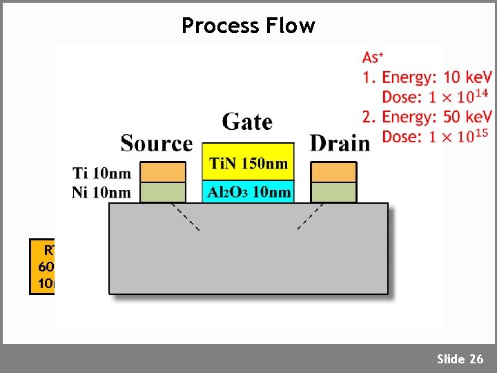
Process Flow RTA 600℃ 10 min Slide 26

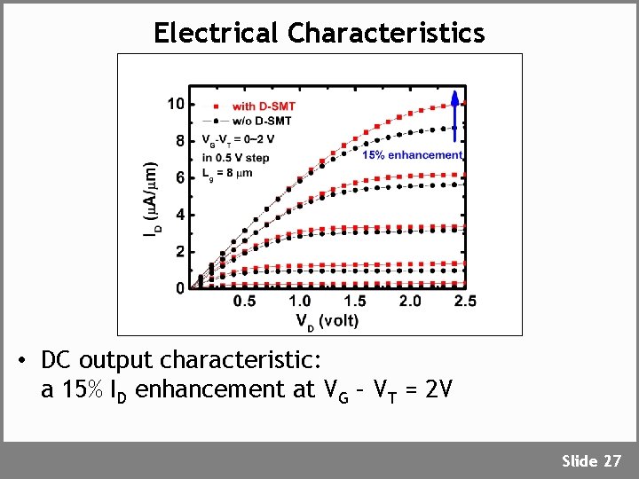
Electrical Characteristics • DC output characteristic: a 15% ID enhancement at VG – VT = 2 V Slide 27

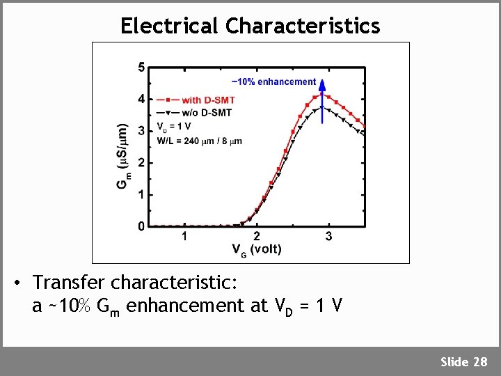
Electrical Characteristics • Transfer characteristic: a ~10% Gm enhancement at VD = 1 V Slide 28

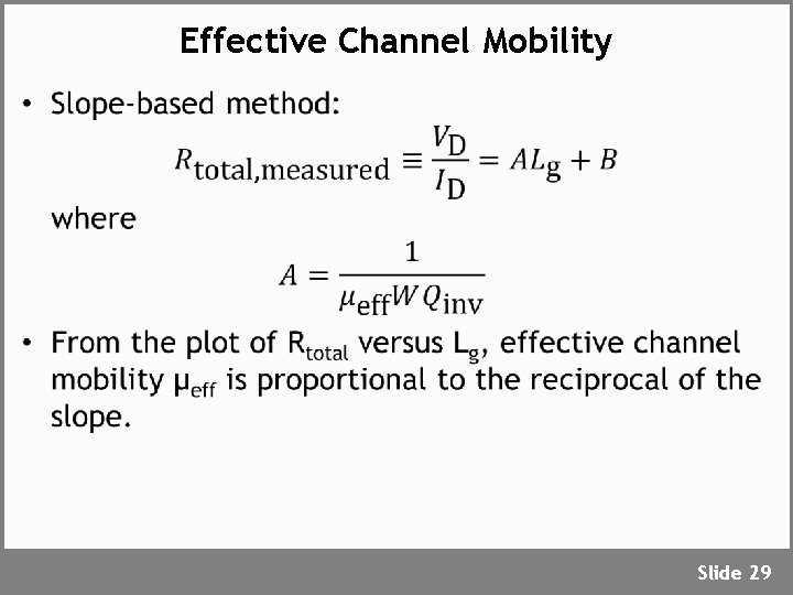
Effective Channel Mobility • Slide 29

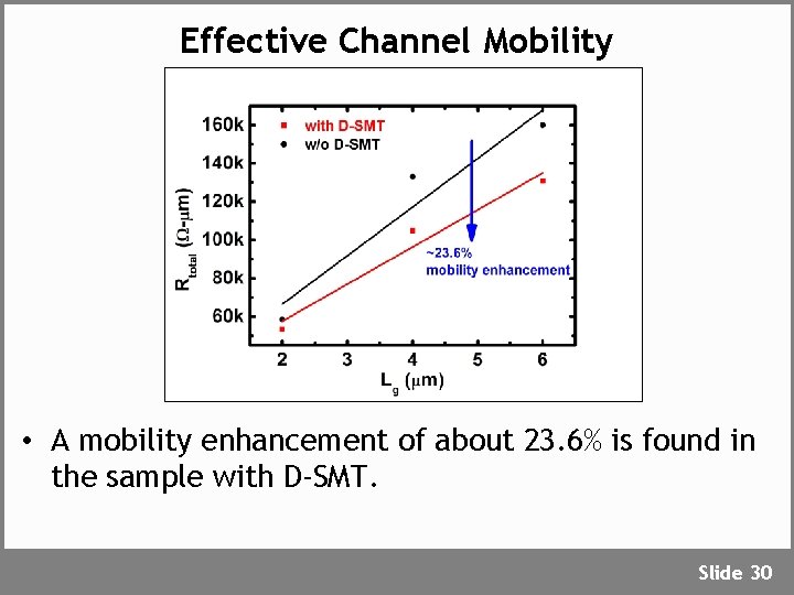
Effective Channel Mobility • A mobility enhancement of about 23. 6% is found in the sample with D-SMT. Slide 30

Outline • • • Introduction Theoretical Background Demonstration of D-SMT on Silicon n. FET Solid-Phase Epitaxial Growth (SPEG) of Germanium Conclusions and Future Works Slide 31

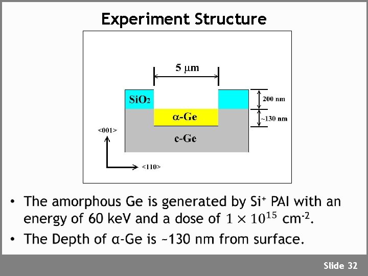
Experiment Structure • Slide 32

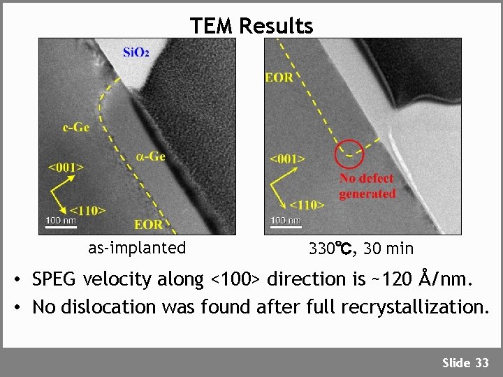
TEM Results as-implanted 330℃, 30 min • SPEG velocity along <100> direction is ~120 Å/nm. • No dislocation was found after full recrystallization. Slide 33

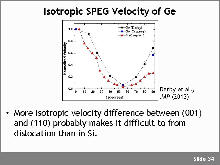
Isotropic SPEG Velocity of Ge Darby et al. , JAP (2013) • More isotropic velocity difference between (001) and (110) probably makes it difficult to from dislocation than in Si. Slide 34

Outline • • • Introduction Theoretical Background Demonstration of D-SMT on Silicon n. FET Solid-Phase Epitaxial Growth (SPEG) of Germanium Conclusions and Future Works Slide 35

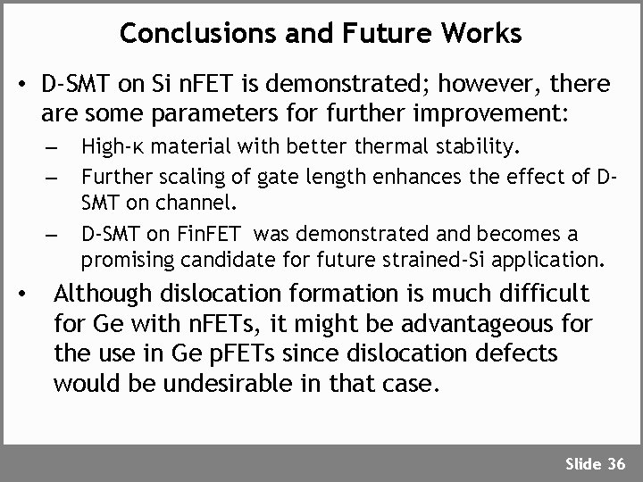
Conclusions and Future Works • D-SMT on Si n. FET is demonstrated; however, there are some parameters for further improvement: – – – • High-κ material with better thermal stability. Further scaling of gate length enhances the effect of DSMT on channel. D-SMT on Fin. FET was demonstrated and becomes a promising candidate for future strained-Si application. Although dislocation formation is much difficult for Ge with n. FETs, it might be advantageous for the use in Ge p. FETs since dislocation defects would be undesirable in that case. Slide 36

Thank you for your listening! Slide 37