Semiconductor Manufacturing Technology Chapter 13 Photolithography Surface Preparation


- Slides: 52

Semiconductor Manufacturing Technology Chapter 13 Photolithography: Surface Preparation to Soft Bake

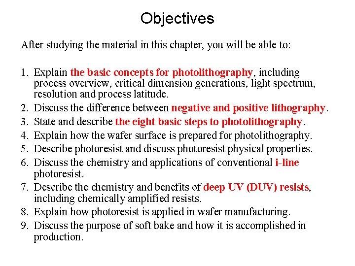
Objectives After studying the material in this chapter, you will be able to: 1. Explain the basic concepts for photolithography, including process overview, critical dimension generations, light spectrum, resolution and process latitude. 2. Discuss the difference between negative and positive lithography. 3. State and describe the eight basic steps to photolithography. 4. Explain how the wafer surface is prepared for photolithography. 5. Describe photoresist and discuss photoresist physical properties. 6. Discuss the chemistry and applications of conventional i-line photoresist. 7. Describe the chemistry and benefits of deep UV (DUV) resists, including chemically amplified resists. 8. Explain how photoresist is applied in wafer manufacturing. 9. Discuss the purpose of soft bake and how it is accomplished in production.

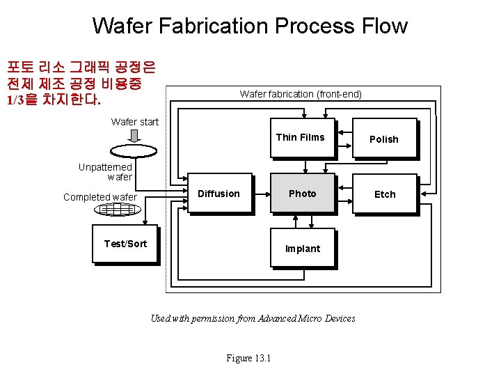
Wafer Fabrication Process Flow 포토 리소 그래픽 공정은 전제 제조 공정 비용중 1/3을 차지한다. Wafer fabrication (front-end) Wafer start Thin Films Polish Photo Etch Unpatterned wafer Completed wafer Diffusion Test/Sort Implant Used with permission from Advanced Micro Devices Figure 13. 1

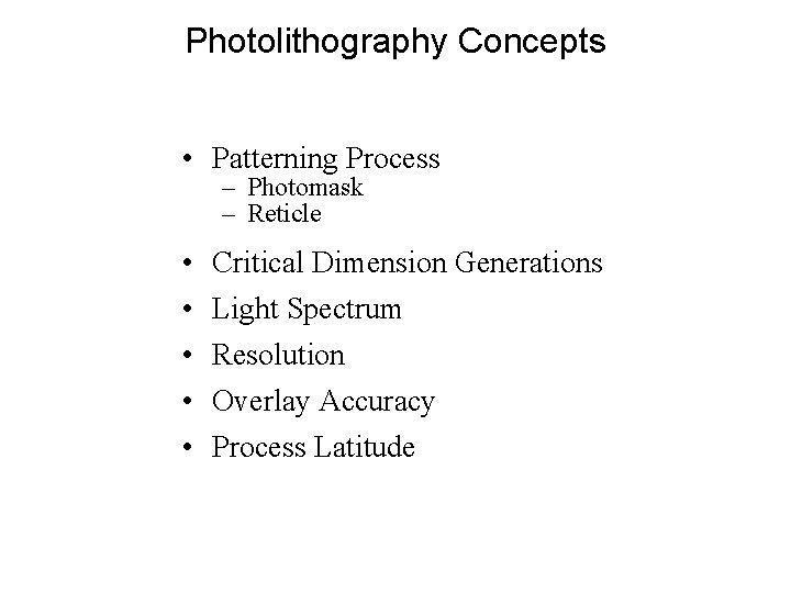
Photolithography Concepts • Patterning Process – Photomask – Reticle • • • Critical Dimension Generations Light Spectrum Resolution Overlay Accuracy Process Latitude

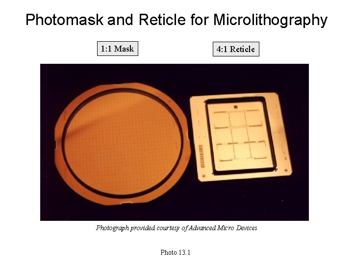
Photomask and Reticle for Microlithography 1: 1 Mask 4: 1 Reticle Photograph provided courtesy of Advanced Micro Devices Photo 13. 1

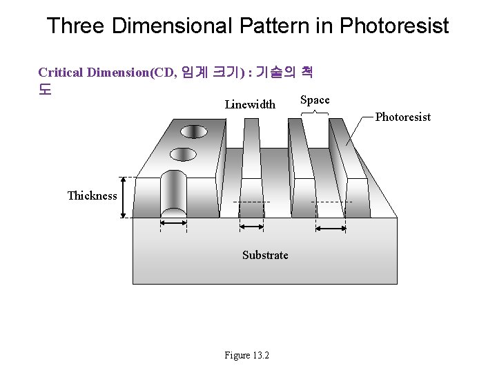
Three Dimensional Pattern in Photoresist Critical Dimension(CD, 임계 크기) : 기술의 척 도 Linewidth Thickness Substrate Figure 13. 2 Space Photoresist

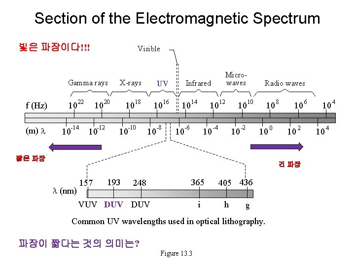
Section of the Electromagnetic Spectrum 빛은 파장이다!!! Visible Gamma rays f (Hz) (m) 10 10 22 -14 10 20 -12 10 X-rays 10 10 -10 Infrared UV 18 10 10 -8 16 Microwaves 10 10 14 10 -6 10 12 -4 10 10 Radio waves 10 -2 10 10 0 짧은 파장 8 10 10 2 긴 파장 (nm) 157 193 248 365 VUV DUV i 405 436 h g Common UV wavelengths used in optical lithography. 파장이 짧다는 것의 의미는? Figure 13. 3 6 10 10 4 4

Important Wavelengths for Photolithography Exposure 사용된 광원의 파장에 따른 명칭!! Table 13. 1 광원의 Source

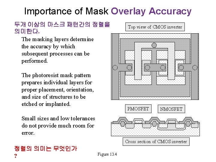
Importance of Mask Overlay Accuracy 두개 이상의 마스크 패턴간의 정렬을 의미한다. The masking layers determine the accuracy by which subsequent processes can be performed. The photoresist mask pattern prepares individual layers for proper placement, orientation, and size of structures to be etched or implanted. Top view of CMOS inverter PMOSFET NMOSFET Small sizes and low tolerances do not provide much room for error. Cross section of CMOS inverter 정렬의 의미는 무엇인가 ? Figure 13. 4

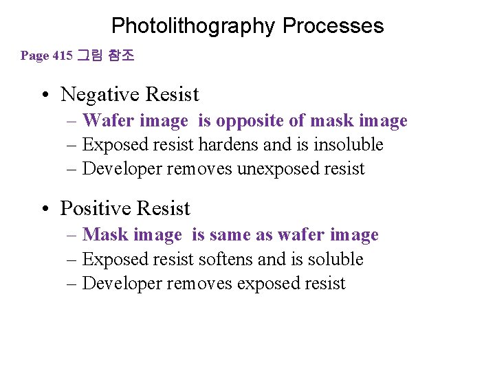
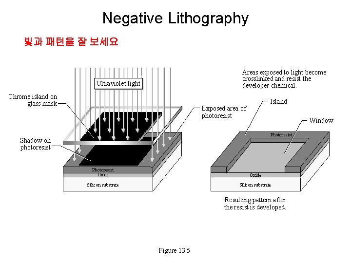
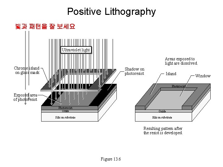
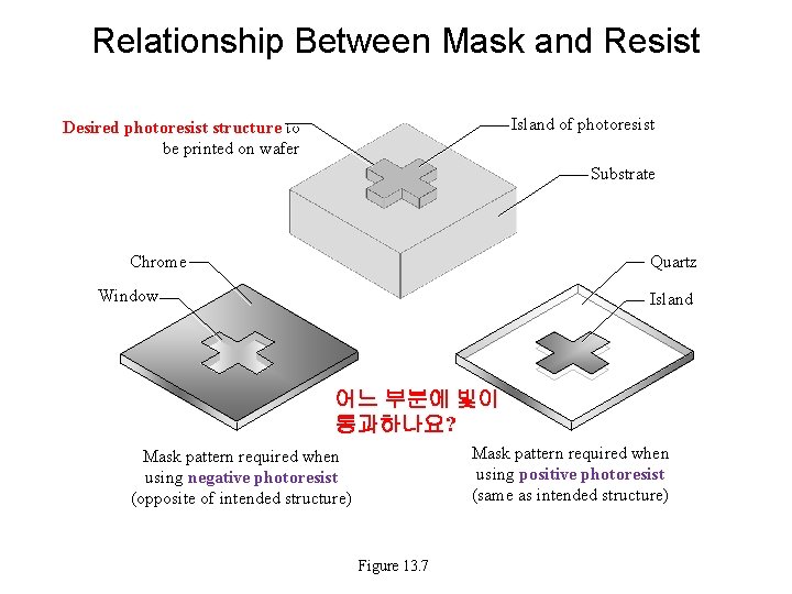
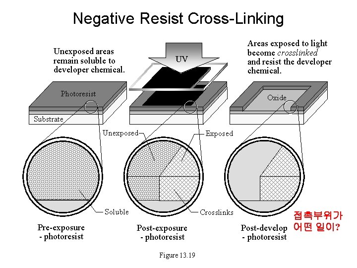
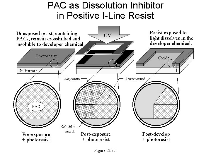
Photolithography Processes Page 415 그림 참조 • Negative Resist – Wafer image is opposite of mask image – Exposed resist hardens and is insoluble – Developer removes unexposed resist • Positive Resist – Mask image is same as wafer image – Exposed resist softens and is soluble – Developer removes exposed resist

Negative Lithography 빛과 패턴을 잘 보세요 Areas exposed to light become crosslinked and resist the developer chemical. Ultraviolet light Chrome island on glass mask Island Exposed area of photoresist Window Photoresist Shadow on photoresist Photoresist Oxide Silicon substrate Resulting pattern after the resist is developed. Figure 13. 5

Positive Lithography 빛과 패턴을 잘 보세요 Ultraviolet light Areas exposed to light are dissolved. Chrome island on glass mask Shadow on photoresist Island photoresist Photoresist Exposed area of photoresist Photoresist oxide Oxide silicon substrate Silicon substrate Silicon Resulting pattern after the resist is developed. Figure 13. 6 Window

Relationship Between Mask and Resist Island of photoresist Desired photoresist structure to be printed on wafer Substrate Chrome Quartz Window Island 어느 부분에 빛이 통과하나요? Mask pattern required when using positive photoresist (same as intended structure) Mask pattern required when using negative photoresist (opposite of intended structure) Figure 13. 7

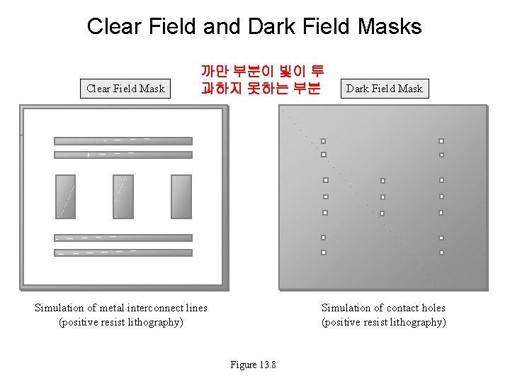
Clear Field and Dark Field Masks Clear Field Mask 까만 부분이 빛이 투 과하지 못하는 부분 Simulation of metal interconnect lines (positive resist lithography) Dark Field Mask Simulation of contact holes (positive resist lithography) Figure 13. 8

Eight Steps of Photolithography 매우 중요 Table 13. 2

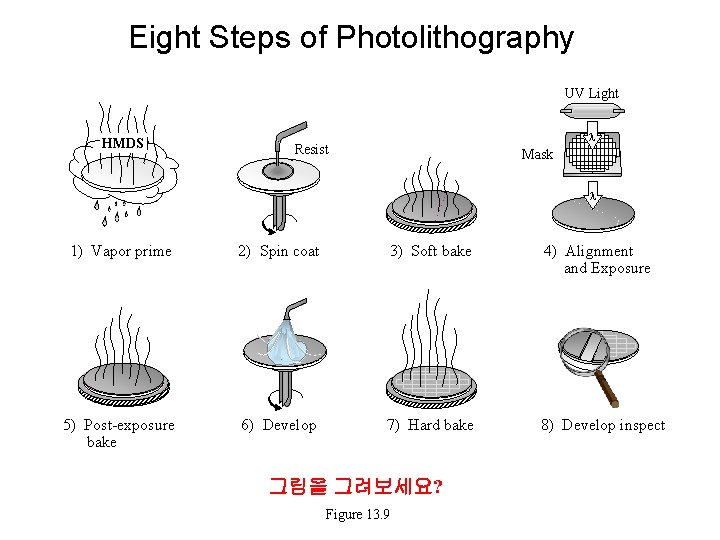
Eight Steps of Photolithography UV Light HMDS Resist Mask 1) Vapor prime 2) Spin coat 3) Soft bake 4) Alignment and Exposure 5) Post-exposure bake 6) Develop 7) Hard bake 8) Develop inspect 그림을 그려보세요? Figure 13. 9

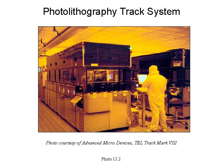
Photolithography Track System Photo courtesy of Advanced Micro Devices, TEL Track Mark VIII Photo 13. 2

Vapor Prime The First Step of Photolithography: • • Promotes Good Photoresist-to-Wafer Adhesion Primes Wafer with Hexamethyldisilazane, HMDS Followed by Dehydration Bake Ensures Wafer Surface is Clean and Dry HMDS는 부착을 증진시키기 위한 물질이다.

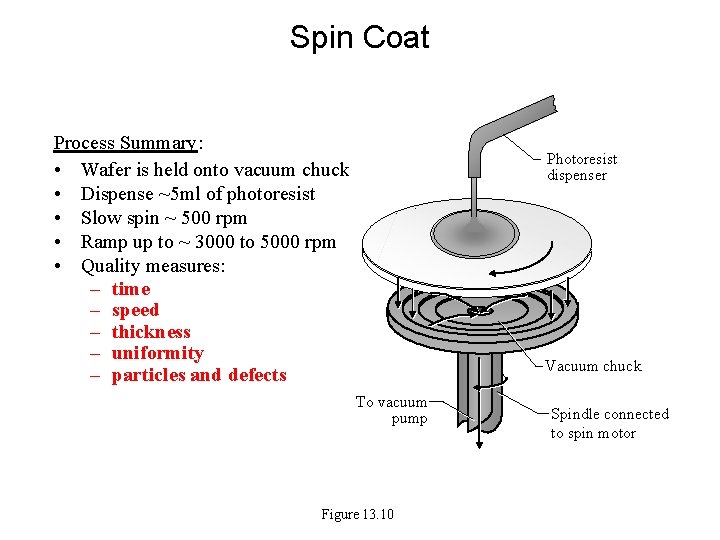
Spin Coat Process Summary: • Wafer is held onto vacuum chuck • Dispense ~5 ml of photoresist • Slow spin ~ 500 rpm • Ramp up to ~ 3000 to 5000 rpm • Quality measures: – time – speed – thickness – uniformity – particles and defects Photoresist dispenser Vacuum chuck To vacuum pump Figure 13. 10 Spindle connected to spin motor

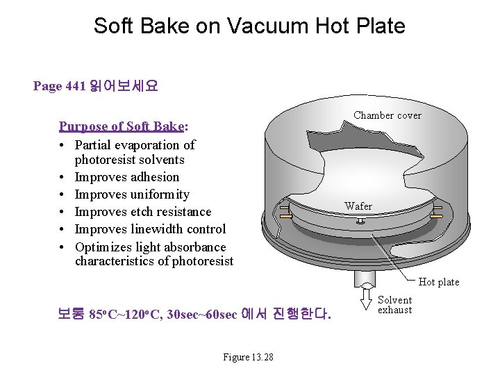
Soft bake Characteristics of Soft Bake: • • • Improves Photoresist-to-Wafer Adhesion Promotes Resist Uniformity on Wafer Improves Linewidth Control During Etch Drives Off Most of Solvent in Photoresist Typical Bake Temperatures are 90 to 100°C – For About 30 Seconds – On a Hot Plate – Followed by Cooling Step on Cold Plate

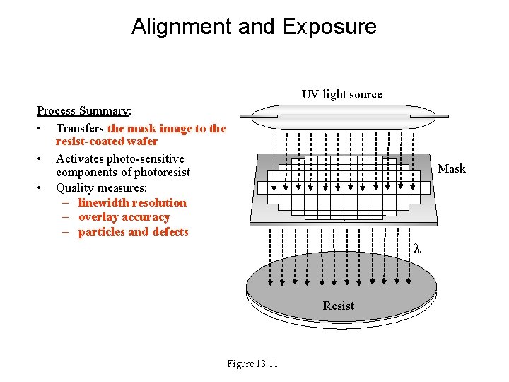
Alignment and Exposure UV light source Process Summary: • Transfers the mask image to the resist-coated wafer • Activates photo-sensitive components of photoresist • Quality measures: – linewidth resolution – overlay accuracy – particles and defects Mask Resist Figure 13. 11

Post-Exposure Bake • Required for Deep UV Resists • Typical Temperatures 100 to 110 C on a hot plate • Immediately after Exposure • Has Become a Virtual Standard for DUV and Standard Resists

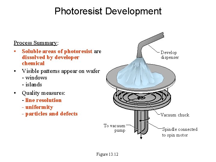
Photoresist Development Process Summary: • Soluble areas of photoresist are dissolved by developer chemical • Visible patterns appear on wafer - windows - islands • Quality measures: - line resolution - uniformity - particles and defects Develop dispenser Vacuum chuck To vacuum pump Figure 13. 12 Spindle connected to spin motor

Hard Bake • • A Post-Development Thermal Bake Evaporate Remaining Solvent Improve Resist-to-Wafer Adhesion Higher Temperature (120 to 140°C) than Soft Bake

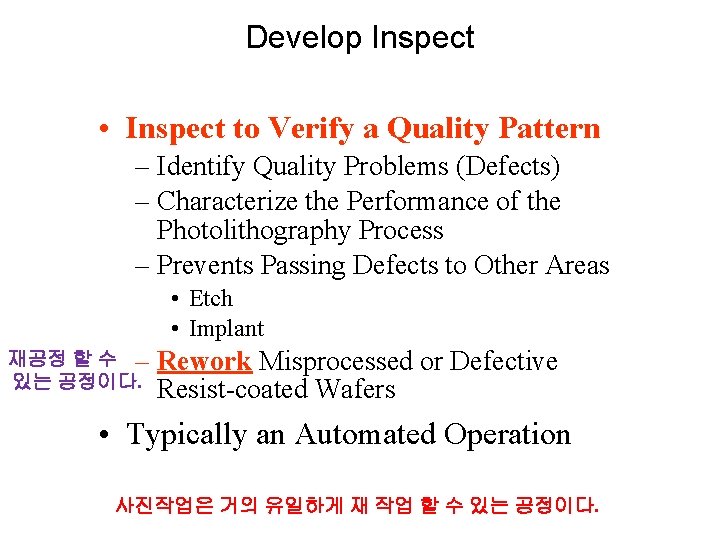
Develop Inspect • Inspect to Verify a Quality Pattern – Identify Quality Problems (Defects) – Characterize the Performance of the Photolithography Process – Prevents Passing Defects to Other Areas • Etch • Implant 재공정 할 수 – 있는 공정이다. Rework Misprocessed or Defective Resist-coated Wafers • Typically an Automated Operation 사진작업은 거의 유일하게 재 작업 할 수 있는 공정이다.

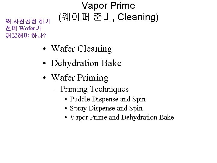
왜 사진공정 하기 전에 Wafer가 깨끗해야 하나? Vapor Prime (웨이퍼 준비, Cleaning) • Wafer Cleaning • Dehydration Bake • Wafer Priming – Priming Techniques • Puddle Dispense and Spin • Spray Dispense and Spin • Vapor Prime and Dehydration Bake

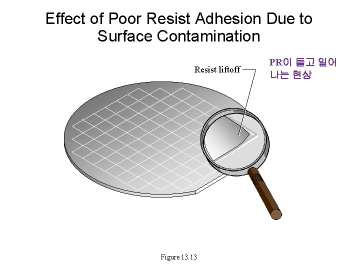
Effect of Poor Resist Adhesion Due to Surface Contamination Resist liftoff Figure 13. 13 PR이 들고 일어 나는 현상

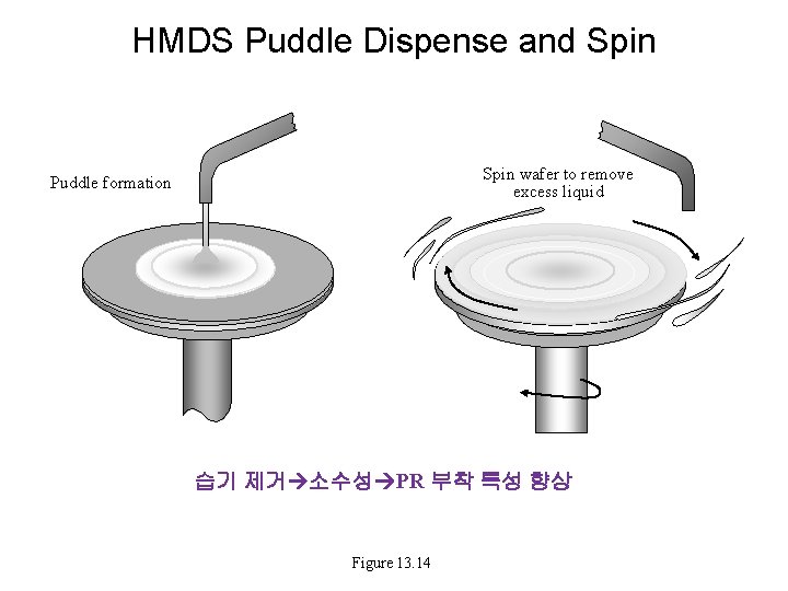
HMDS Puddle Dispense and Spin wafer to remove excess liquid Puddle formation 습기 제거 소수성 PR 부착 특성 향상 Figure 13. 14

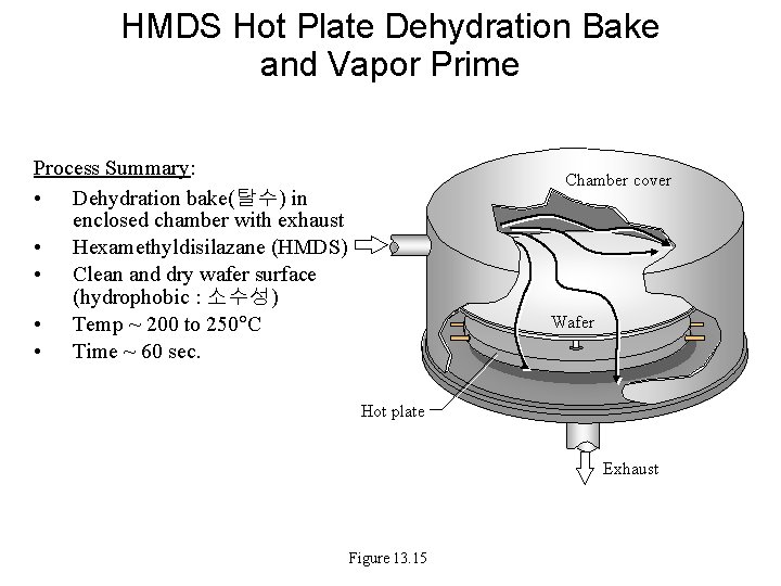
HMDS Hot Plate Dehydration Bake and Vapor Prime Process Summary: • Dehydration bake(탈수) in enclosed chamber with exhaust • Hexamethyldisilazane (HMDS) • Clean and dry wafer surface (hydrophobic : 소수성) • Temp ~ 200 to 250 C • Time ~ 60 sec. Chamber cover Wafer Hot plate Exhaust Figure 13. 15

The Purpose of Photoresist in Wafer Fab • To transfer the mask pattern to the photoresist on the top layer of the wafer surface • To protect the underlying material during subsequent processing e. g. etch or ion implantation.

Successive Reductions in CDs Lead to Progressive Improvements in Photoresist • Better image definition (resolution). • Better adhesion to semiconductor wafer surfaces. • Better uniformity characteristics. • Increased process latitude (less sensitivity to process variations).

Spin Coat • Photoresist – Types of Photoresist – Negative Versus Positive Photoresists • Photoresist Physical Properties • Conventional I-Line Photoresists – Negative I-Line Photoresists – Positive I-Line Photoresists • Deep UV (DUV) Photoresists • Photoresist Dispensing Methods

Types of Photoresists • Two Types of Photoresist – Positive Resist – Negative Resist • CD Capability – Conventional Resist – Deep UV Resist • Process Applications – Non-critical Layers – Critical Layers

Negative Versus Positive Resists • Negative Resist – Wafer image is opposite of mask image – Exposed resist hardens and is insoluble – Developer removes unexposed resist • Positive Resist – Mask image is same as wafer image – Exposed resist softens and is soluble – Developer removes exposed resist • Resolution Issues • Clear Field Versus Dark Field Masks

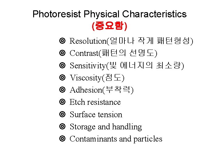
Photoresist Physical Characteristics (중요함) ¥ ¥ ¥ ¥ ¥ Resolution(얼마나 작게 패턴형성) Contrast(패턴의 선명도) Sensitivity(빛 에너지의 최소량) Viscosity(점도) Adhesion(부착력) Etch resistance Surface tension Storage and handling Contaminants and particles

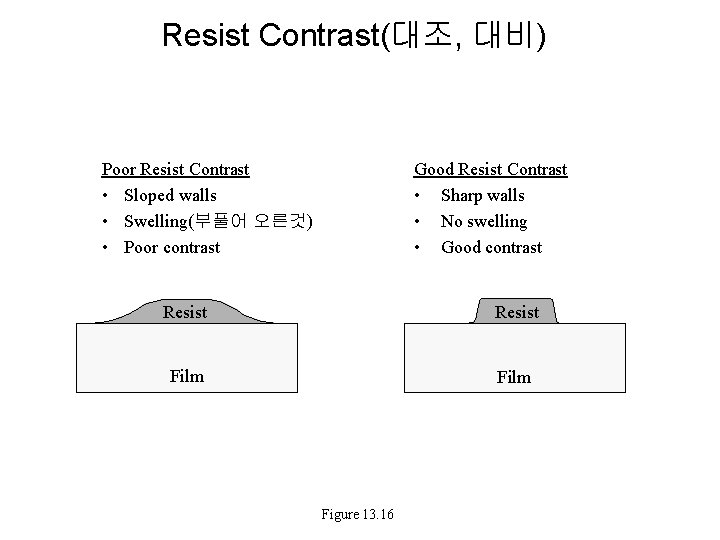
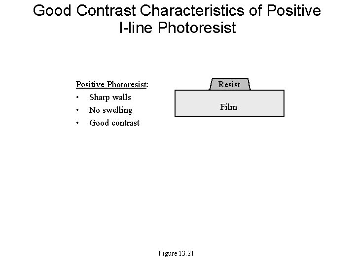
Resist Contrast(대조, 대비) Poor Resist Contrast • Sloped walls • Swelling(부풀어 오른것) • Poor contrast Good Resist Contrast • Sharp walls • No swelling • Good contrast Resist Film Figure 13. 16

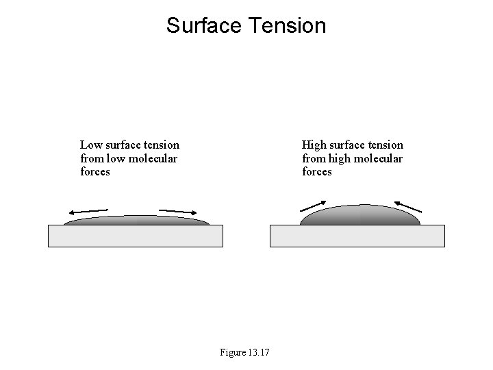
Surface Tension Low surface tension from low molecular forces High surface tension from high molecular forces Figure 13. 17

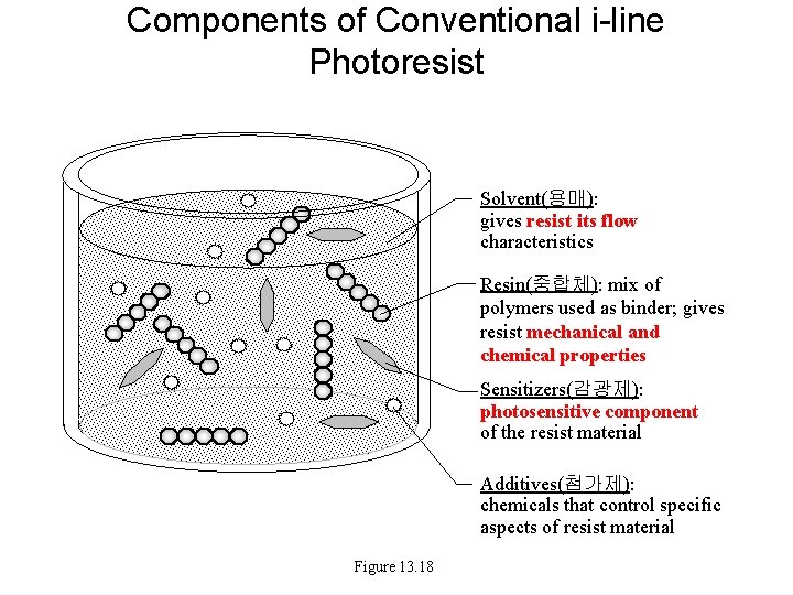
Components of Conventional i-line Photoresist Solvent(용매): gives resist its flow characteristics Resin(중합체): mix of polymers used as binder; gives resist mechanical and chemical properties Sensitizers(감광제): photosensitive component of the resist material Additives(첨가제): chemicals that control specific aspects of resist material Figure 13. 18

Negative Resist Cross-Linking Unexposed areas remain soluble to developer chemical. Areas exposed to light become crosslinked and resist the developer chemical. UV Photoresist Oxide Substrate Unexposed Exposed Soluble Pre-exposure - photoresist Crosslinks Post-exposure - photoresist Figure 13. 19 접촉부위가 Post-develop 어떤 일이? - photoresist

PAC as Dissolution Inhibitor in Positive I-Line Resist Unexposed resist, containing PACs, remain crosslinked and insoluble to developer chemical. Resist exposed to light dissolves in the developer chemical. UV Photoresist Oxide Substrate Exposed Unexposed PAC Pre-exposure + photoresist Soluble resist Post-exposure + photoresist Figure 13. 20 Post-develop + photoresist

Good Contrast Characteristics of Positive I-line Photoresist Positive Photoresist: • Sharp walls • No swelling • Good contrast Resist Film Figure 13. 21

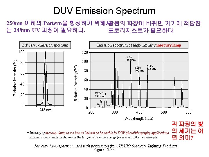
DUV Emission Spectrum 250 nm 이하의 Pattern을 형성하기 위해서 광원의 파장이 바뀌면 거기에 적당한 는 248 nm UV 파장이 필요하다. 포토리지스트가 필요하다 Emission spectrum of high-intensity mercury lamp Kr. F laser emission spectrum 120 60 40 20 0 i-line 365 nm 100 80 Relative Intensity (%) 100 248 nm h-line 405 nm 80 g-line 436 nm 60 40 DUV* 248 nm 20 0 200 300 400 500 600 Wavelength (nm) 각 파장의 빛 * Intensity of mercury lamp is too low at 248 nm to be usable in DUV photolithography applications. 의 세기는 어 Excimer lasers, such as shown on the left provide more energy for a given DUV wavelength. 떤 의미? Mercury lamp spectrum used with permission from USHIO Specialty Lighting Products Figure 13. 22

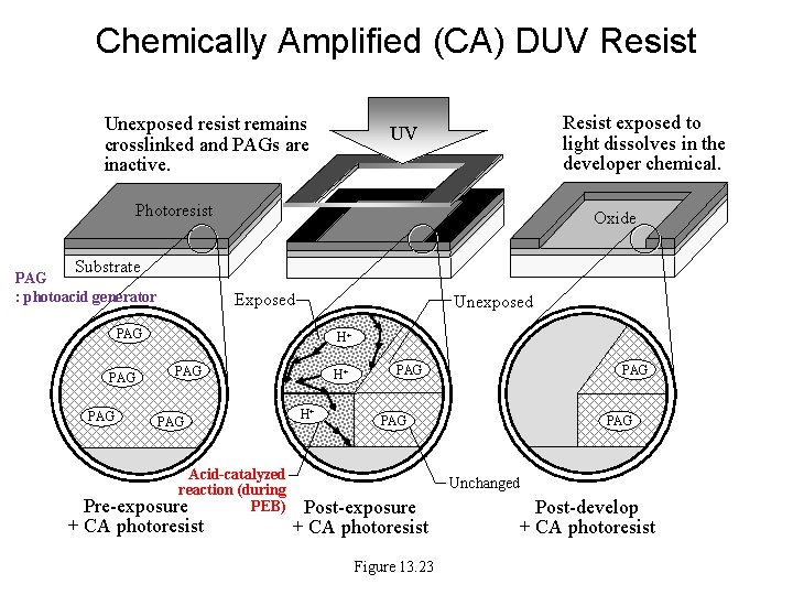
Chemically Amplified (CA) DUV Resist Unexposed resist remains crosslinked and PAGs are inactive. Resist exposed to light dissolves in the developer chemical. UV Photoresist Oxide Substrate PAG : photoacid generator Exposed Unexposed PAG PAG H+ PAG Acid-catalyzed reaction (during PEB) Pre-exposure + CA photoresist H+ H+ PAG PAG Unchanged Post-exposure + CA photoresist Figure 13. 23 Post-develop + CA photoresist

Exposure Steps for Chemically-Amplified DUV Resist Table 13. 5

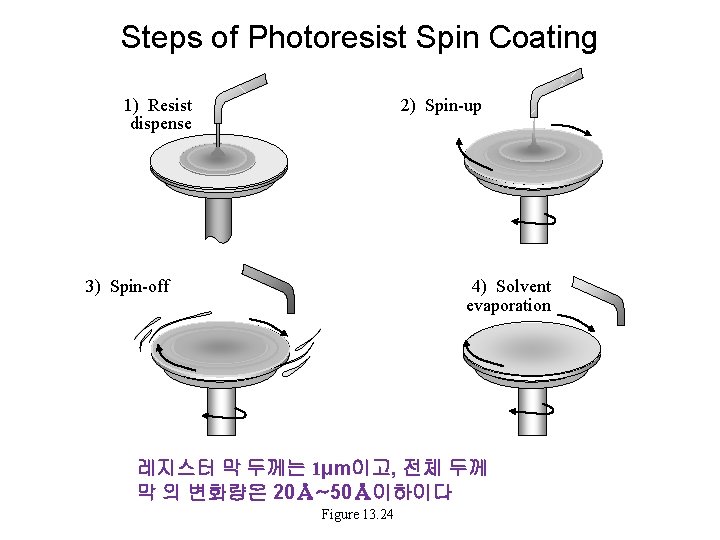
Steps of Photoresist Spin Coating 1) Resist dispense 2) Spin-up 4) Solvent evaporation 3) Spin-off 레지스터 막 두께는 1μm이고, 전체 두께 막 의 변화량은 20Å~50Å이하이다 Figure 13. 24

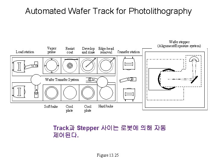
Automated Wafer Track for Photolithography Load station Vapor prime Resist coat Develop Edge-bead and rinse removal Transfer station Wafer stepper (Alignment/Exposure system) Wafer Transfer System Soft bake Cool plate Hard bake Track과 Stepper 사이는 로봇에 의해 자동 제어된다. Figure 13. 25

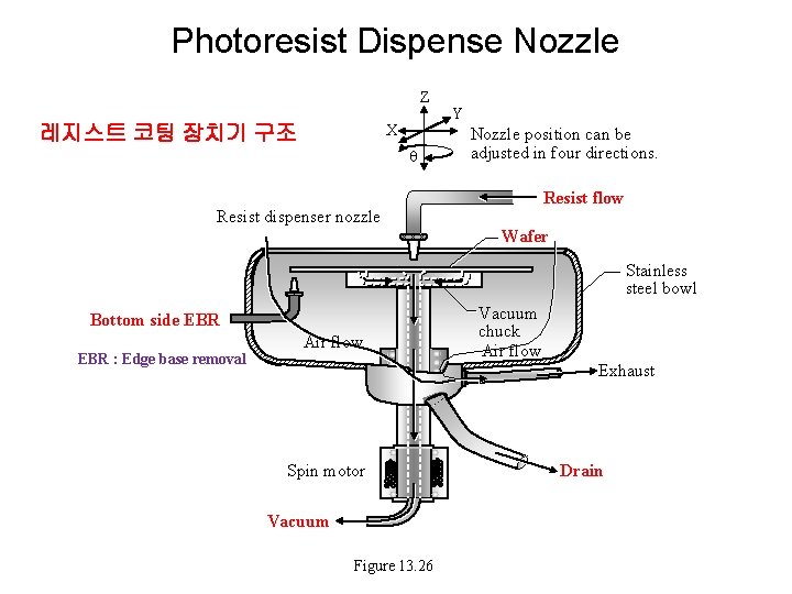
Photoresist Dispense Nozzle Z X 레지스트 코팅 장치기 구조 q Y Nozzle position can be adjusted in four directions. Resist flow Resist dispenser nozzle Wafer Stainless steel bowl Bottom side EBR : Edge base removal Air flow Spin motor Vacuum Figure 13. 26 Vacuum chuck Air flow Exhaust Drain

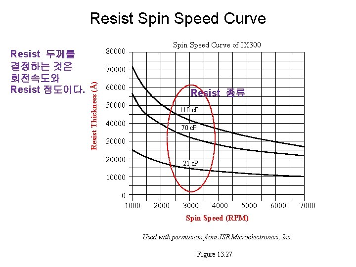
Resist Spin Speed Curve 80000 70000 Resist Thickness (Å) Resist 두께를 결정하는 것은 회전속도와 Resist 점도이다. Spin Speed Curve of IX 300 60000 Resist 종류 50000 110 c. P 40000 70 c. P 30000 21 c. P 10000 0 1000 2000 3000 4000 5000 6000 Spin Speed (RPM) Used with permission from JSR Microelectronics, Inc. Figure 13. 27 7000

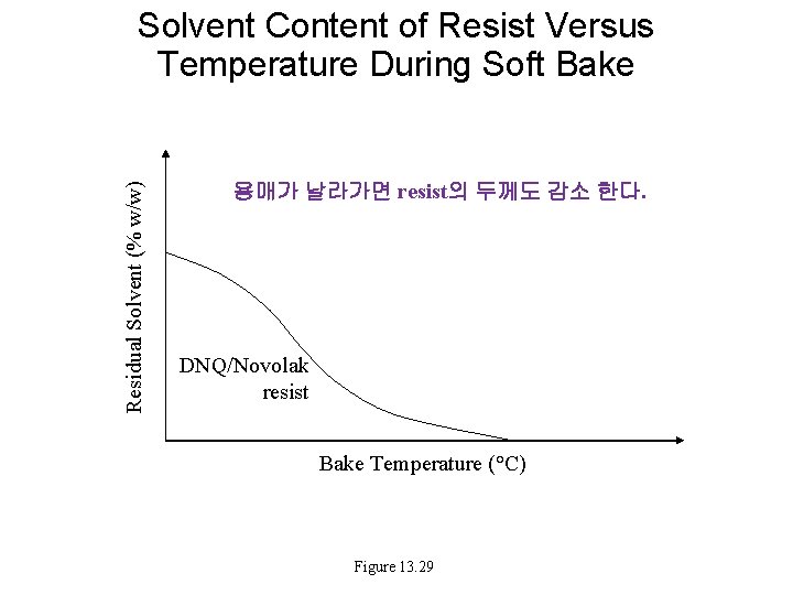
Soft Bake on Vacuum Hot Plate Page 441 읽어보세요 Purpose of Soft Bake: • Partial evaporation of photoresist solvents • Improves adhesion • Improves uniformity • Improves etch resistance • Improves linewidth control • Optimizes light absorbance characteristics of photoresist Chamber cover Wafer Hot plate 보통 85 o. C~120 o. C, 30 sec~60 sec 에서 진행한다. Figure 13. 28 Solvent exhaust

Residual Solvent (% w/w) Solvent Content of Resist Versus Temperature During Soft Bake 용매가 날라가면 resist의 두께도 감소 한다. DNQ/Novolak resist Bake Temperature (°C) Figure 13. 29


Chapter 13 Review • • Quality Measures Troubleshooting Summary Key Terms Review Questions Equipment Suppliers’ Web Sites References 362 363 364 364 365