Photolithography and resolution enhancement techniques RET 1 2

- Slides: 47

Photolithography and resolution enhancement techniques (RET) 1. 2. 3. 4. 5. 6. Photolithography and resolution limit Immersion lithography Off-axis illumination (OAI) Phase-shift mask (PSM) Optical proximity correction (OPC) Double processing ECE 730: Fabrication in the nanoscale: principles, technology and applications Instructor: Bo Cui, ECE, University of Waterloo; http: //ece. uwaterloo. ca/~bcui/ Textbook: Nanofabrication: principles, capabilities and limits, by Zheng Cui

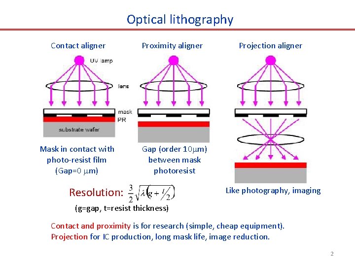
Optical lithography Contact aligner Proximity aligner Mask in contact with photo-resist film (Gap=0 m) Gap (order 10 m) between mask photoresist Resolution: Projection aligner Like photography, imaging (g=gap, t=resist thickness) Contact and proximity is for research (simple, cheap equipment). Projection for IC production, long mask life, image reduction. 2

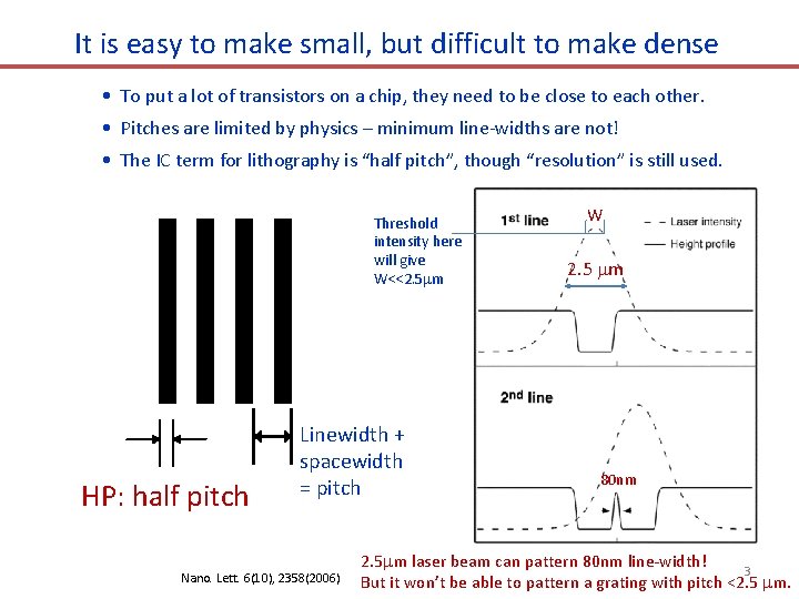
It is easy to make small, but difficult to make dense • To put a lot of transistors on a chip, they need to be close to each other. • Pitches are limited by physics – minimum line-widths are not! • The IC term for lithography is “half pitch”, though “resolution” is still used. Threshold intensity here will give W<<2. 5 m HP: half pitch Linewidth + spacewidth = pitch Nano. Lett. 6(10), 2358(2006) W 2. 5 m 80 nm 2. 5 m laser beam can pattern 80 nm line-width! 3 But it won’t be able to pattern a grating with pitch <2. 5 m.

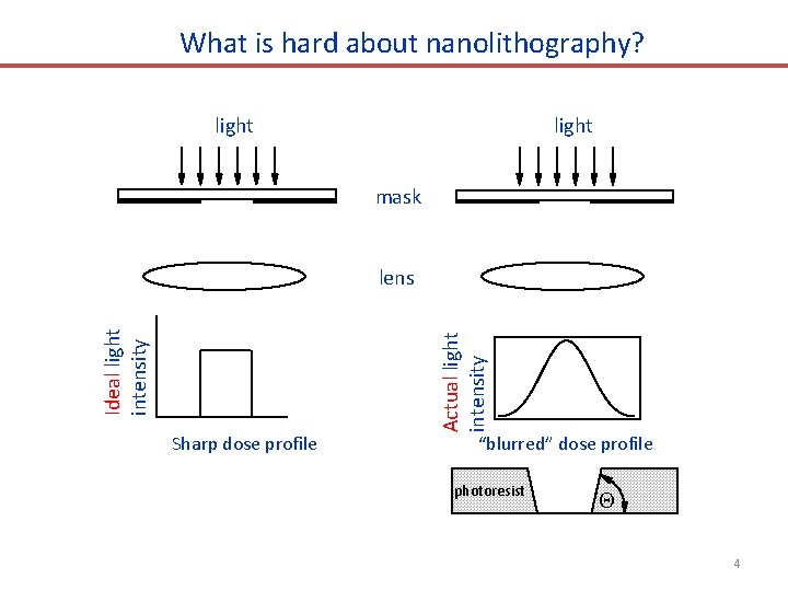
What is hard about nanolithography? light mask Sharp dose profile Actual light intensity Ideal light intensity lens “blurred” dose profile photoresist Q 4

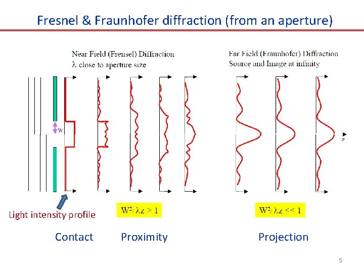
Fresnel & Fraunhofer diffraction (from an aperture) Light intensity profile Contact Proximity Projection 5

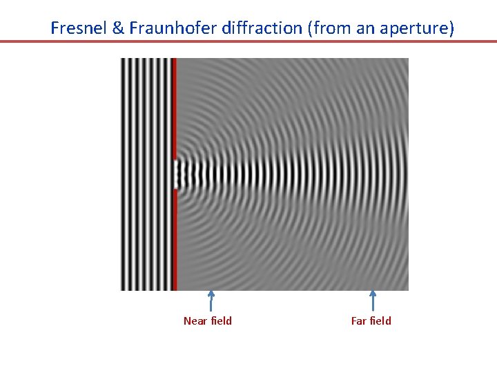
Fresnel & Fraunhofer diffraction (from an aperture) Near field Far field

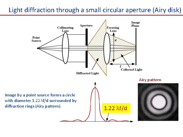
Light diffraction through a small circular aperture (Airy disk) Airy pattern Image by a point source forms a circle with diameter 1. 22 f/d surrounded by diffraction rings (Airy pattern). 1. 22 f/d

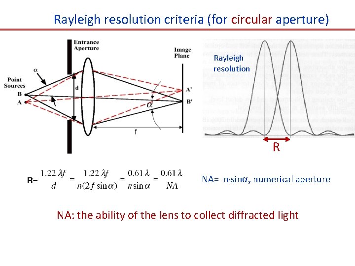
Rayleigh resolution criteria (for circular aperture) Rayleigh resolution R NA= n sin , numerical aperture NA: the ability of the lens to collect diffracted light

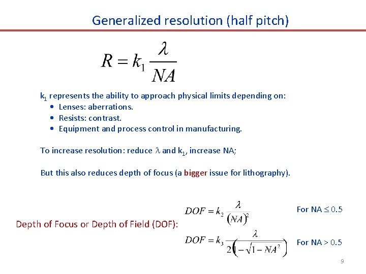
Generalized resolution (half pitch) k 1 represents the ability to approach physical limits depending on: • Lenses: aberrations. • Resists: contrast. • Equipment and process control in manufacturing. To increase resolution: reduce and k 1, increase NA; But this also reduces depth of focus (a bigger issue for lithography). For NA 0. 5 Depth of Focus or Depth of Field (DOF): For NA > 0. 5 9

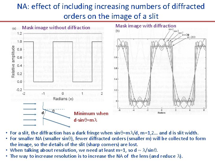
NA: effect of including increasing numbers of diffracted orders on the image of a slit Mask image without diffraction Mask image with diffraction 0 d Minimum when d sin =m • For a slit, the diffraction has a dark fringe when sin =m /d, m=1, 2… and d is slit width. • For smaller NA (smaller sin ), fewer diffracted orders (smaller m) will be collected to form the image, so the details of the slit (sharp corners) are lost. • When talking about resolution, we need at least m=1, so d /sin. • The way to increase resolution is to increase the NA of the lens (and reduce ).

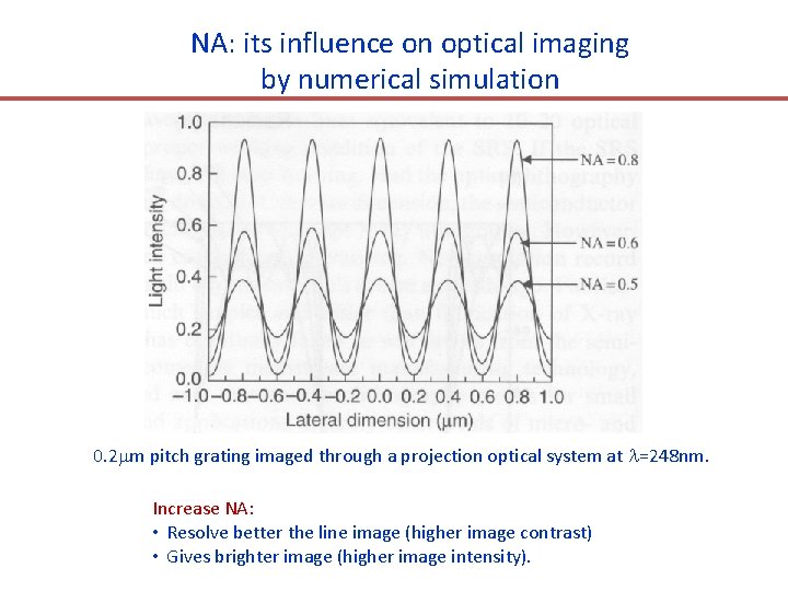
NA: its influence on optical imaging by numerical simulation 0. 2 m pitch grating imaged through a projection optical system at =248 nm. Increase NA: • Resolve better the line image (higher image contrast) • Gives brighter image (higher image intensity).

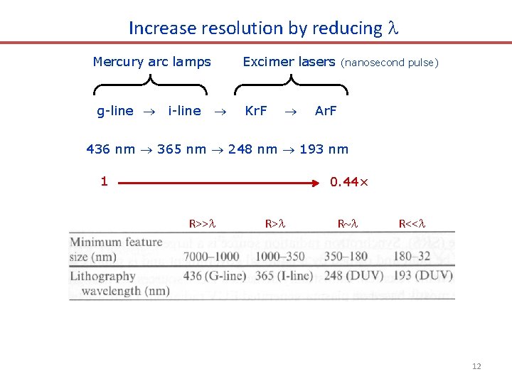
Increase resolution by reducing Mercury arc lamps g-line i-line Excimer lasers Kr. F (nanosecond pulse) Ar. F 436 nm 365 nm 248 nm 193 nm 1 0. 44× R>> R R<< 12

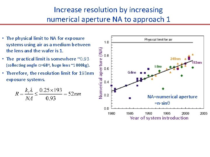
• The physical limit to NA for exposure systems using air as a medium between the lens and the wafer is 1. • The practical limit is somewhere ~0. 93 (collecting angle =68 o, huge lens ~1000 kg). • Therefore, the resolution limit for 193 nm exposure systems. Numerical aperture (NA) Increase resolution by increasing numerical aperture NA to approach 1 NA=numerical aperture =n sin Year of system introduction

Photolithography and resolution enhancement techniques (RET) 1. 2. 3. 4. 5. 6. Photolithography and resolution limit Immersion lithography Off-axis illumination (OAI) Phase-shift mask (PSM) Optical proximity correction (OPC) Double processing

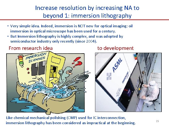
Increase resolution by increasing NA to beyond 1: immersion lithography • Very simple idea. Indeed, immersion is NOT new for optical imaging: oil immersion in optical microscope has been used for a century. • But Immersion lithography is highly complex, and was adopted by semiconductor industry only recently (since 2004). From research idea to development Like chemical mechanical polishing (CMP) used for IC interconnection, immersion lithography has been considered as impractical at the beginning. 15

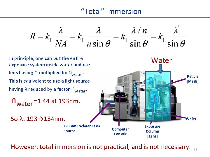
“Total” immersion Water In principle, one can put the entire exposure system inside water and use lens having n multiplied by nwater. Reticle (Mask) This is equivalent to use a light source having reduced by a factor nwater =1. 44 at 193 nm. So : 193→ 134 nm. 193 nm Excimer Laser Source Wafer Computer Console Exposure Column (Lens) However, total immersion is not practical, and is not necessary. 16

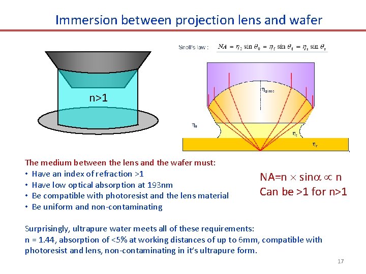
Immersion between projection lens and wafer n>1 The medium between the lens and the wafer must: • Have an index of refraction >1 • Have low optical absorption at 193 nm • Be compatible with photoresist and the lens material • Be uniform and non-contaminating NA=n sin n Can be >1 for n>1 Surprisingly, ultrapure water meets all of these requirements: n = 1. 44, absorption of <5% at working distances of up to 6 mm, compatible with photoresist and lens, non-contaminating in it’s ultrapure form. 17

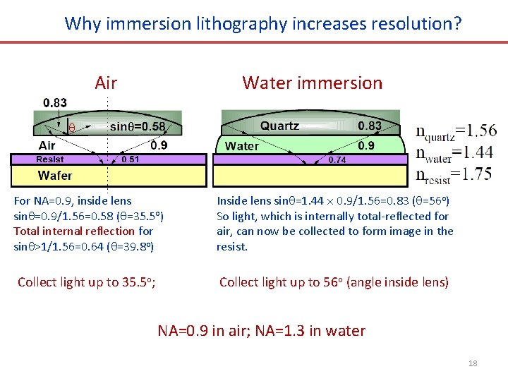
Why immersion lithography increases resolution? Air Water immersion For NA=0. 9, inside lens sin =0. 9/1. 56=0. 58 ( =35. 5 o) Total internal reflection for sin >1/1. 56=0. 64 ( =39. 8 o) Inside lens sin =1. 44 0. 9/1. 56=0. 83 ( =56 o) So light, which is internally total-reflected for air, can now be collected to form image in the resist. Collect light up to 35. 5 o; Collect light up to 56 o (angle inside lens) NA=0. 9 in air; NA=1. 3 in water 18

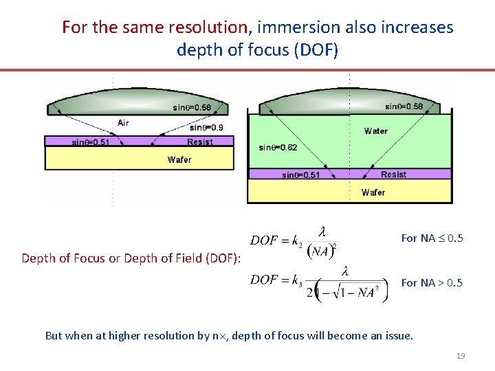
For the same resolution, immersion also increases depth of focus (DOF) For NA 0. 5 Depth of Focus or Depth of Field (DOF): For NA > 0. 5 But when at higher resolution by n , depth of focus will become an issue. 19

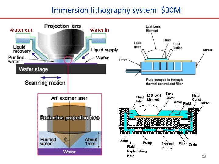
Immersion lithography system: $30 M Water out Water in 20

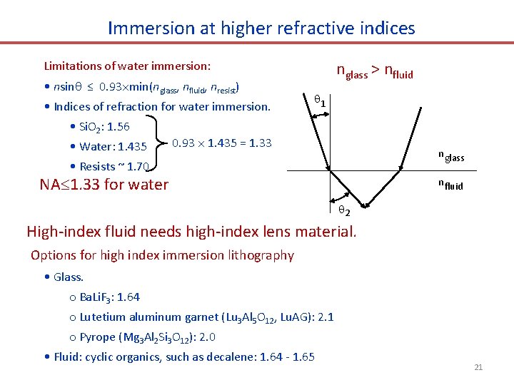
Immersion at higher refractive indices nglass > nfluid Limitations of water immersion: • nsin ≤ 0. 93 min(nglass, nfluid, nresist) • Indices of refraction for water immersion. • Si. O 2: 1. 56 • Water: 1. 435 1 0. 93 1. 435 = 1. 33 n glass • Resists ~ 1. 70 NA 1. 33 for water n fluid 2 High-index fluid needs high-index lens material. Options for high index immersion lithography • Glass. o Ba. Li. F 3: 1. 64 o Lutetium aluminum garnet (Lu 3 Al 5 O 12, Lu. AG): 2. 1 o Pyrope (Mg 3 Al 2 Si 3 O 12): 2. 0 • Fluid: cyclic organics, such as decalene: 1. 64 - 1. 65 21

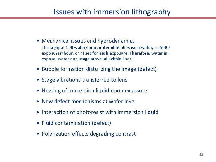
Issues with immersion lithography • Mechanical issues and hydrodynamics Throughput 100 wafer/hour, order of 50 dies each wafer, so 5000 exposures/hour, or <1 sec for each exposure. Therefore, water in, expose, water out, stage move, all within 1 sec. • Bubble formation disturbing the image (defect) • Stage vibrations transferred to lens • Heating of immersion liquid upon exposure • New defect mechanisms at wafer level • Interaction of photoresist with immersion liquid • Fluid contamination (defect) • Polarization effects degrading contrast 22

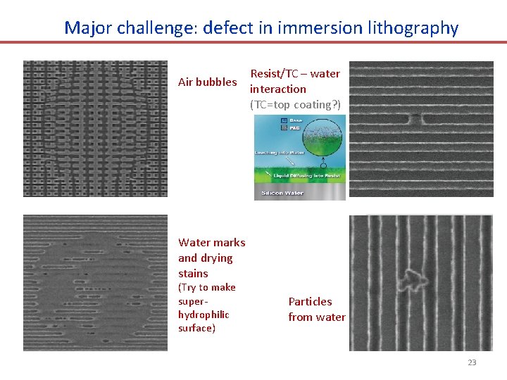
Major challenge: defect in immersion lithography Air bubbles Resist/TC – water interaction (TC=top coating? ) Water marks and drying stains (Try to make superhydrophilic surface) Particles from water 23

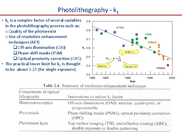
Photolithography - k 1 • k 1 is a complex factor of several variables in the photolithography process such as: o Quality of the photoresist o Use of resolution enhancement techniques (RET) q Off-axis illumination (OAI) q Phase shift masks (PSM) q Optical proximity correction (OPC). • The practical lower limit for k 1 is thought to be about 0. 25 (for single exposure).

Photolithography and resolution enhancement techniques (RET) 1. 2. 3. 4. 5. 6. Photolithography and resolution limit Immersion lithography Off-axis illumination (OAI) Phase-shift mask (PSM) Optical proximity correction (OPC) Double processing

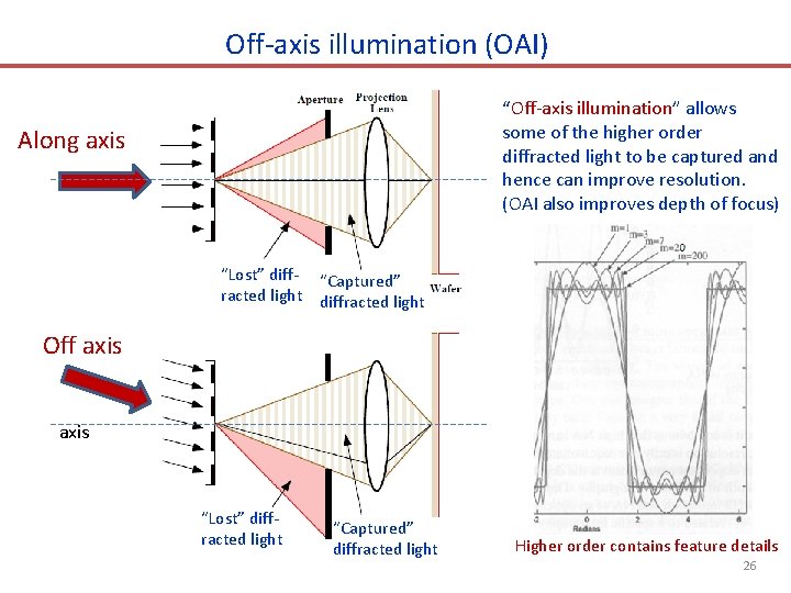
Off-axis illumination (OAI) “Off-axis illumination” allows some of the higher order diffracted light to be captured and hence can improve resolution. (OAI also improves depth of focus) Along axis “Lost” diffracted light “Captured” diffracted light Off axis “Lost” diffracted light “Captured” diffracted light Higher order contains feature details 26

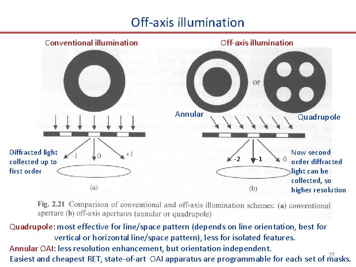
Off-axis illumination Conventional illumination Off-axis illumination Annular Diffracted light collected up to first order Quadrupole -2 -1 Now second order diffracted light can be collected, so higher resolution Quadrupole: most effective for line/space pattern (depends on line orientation, best for vertical or horizontal line/space pattern), less for isolated features. Annular OAI: less resolution enhancement, but orientation independent. 27 Easiest and cheapest RET, state-of-art OAI apparatus are programmable for each set of masks.

Photolithography and resolution enhancement techniques (RET) 1. 2. 3. 4. 5. 6. Photolithography and resolution limit Immersion lithography Off-axis illumination (OAI) Phase-shift mask (PSM) Optical proximity correction (OPC) Double processing

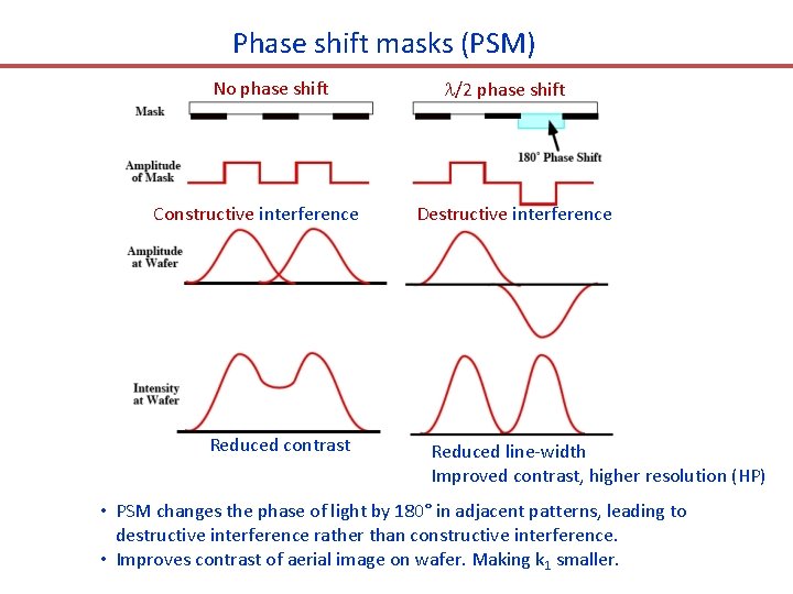
Phase shift masks (PSM) No phase shift Constructive interference Reduced contrast /2 phase shift Destructive interference Reduced line-width Improved contrast, higher resolution (HP) • PSM changes the phase of light by 180° in adjacent patterns, leading to destructive interference rather than constructive interference. • Improves contrast of aerial image on wafer. Making k 1 smaller.

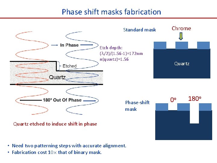
Phase shift masks fabrication Standard mask Etch depth: ( /2)/(1. 56 -1)=172 nm n(quartz)=1. 56 Phase-shift mask Quartz etched to induce shift in phase • Need two patterning steps with accurate alignment. • Fabrication cost 10 that of binary mask. Chrome Quartz 0 o 180 o

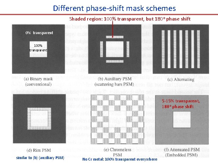
Different phase-shift mask schemes Shaded region: 100% transparent, but 180 o phase shift 0% transparent 100% transparent 5 -15% transparent, 180 o phase shift similar to (b) (auxiliary PSM) No Cr metal: 100% transparent everywhere

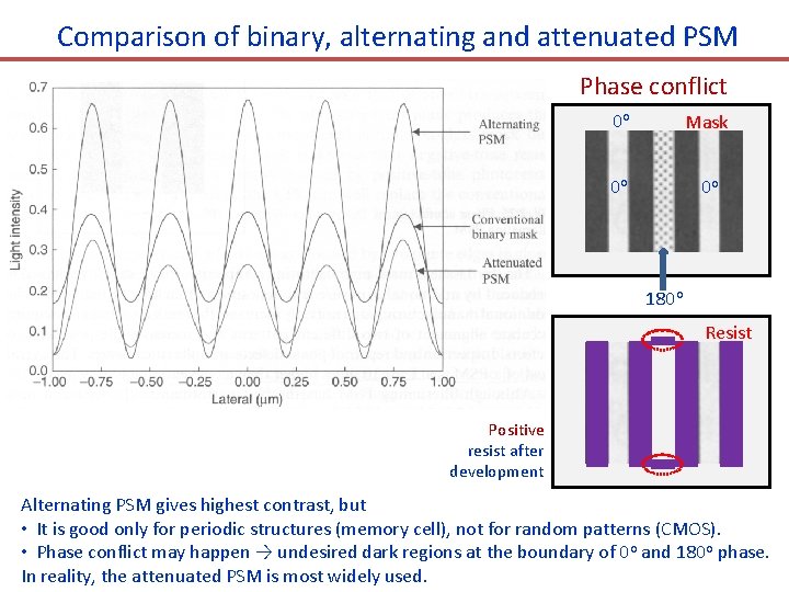
Comparison of binary, alternating and attenuated PSM Phase conflict 0 o Mask 0 o 0 o 180 o Resist Positive resist after development Alternating PSM gives highest contrast, but • It is good only for periodic structures (memory cell), not for random patterns (CMOS). • Phase conflict may happen → undesired dark regions at the boundary of 0 o and 180 o phase. In reality, the attenuated PSM is most widely used.

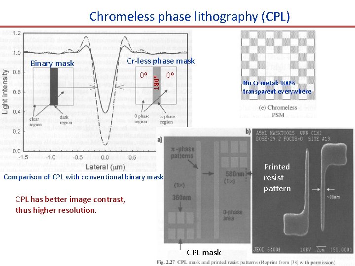
Chromeless phase lithography (CPL) Cr-less phase mask 0 o 180 o Binary mask 0 o No Cr metal: 100% transparent everywhere Printed resist pattern Comparison of CPL with conventional binary mask CPL has better image contrast, thus higher resolution. CPL mask

Photolithography and resolution enhancement techniques (RET) 1. 2. 3. 4. 5. 6. Photolithography and resolution limit Immersion lithography Off-axis illumination (OAI) Phase-shift mask (PSM) Optical proximity correction (OPC) Double processing

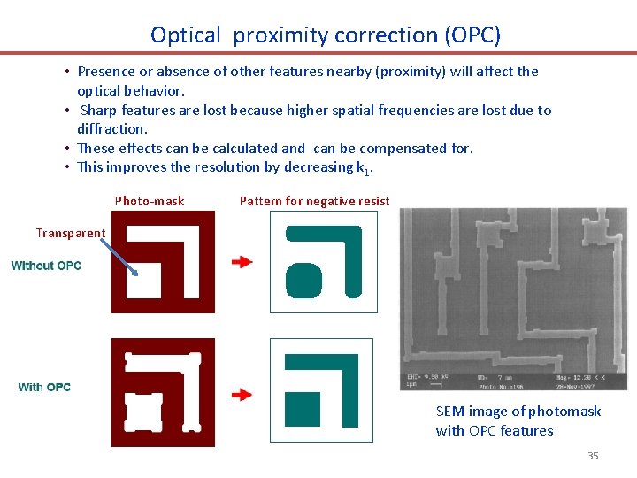
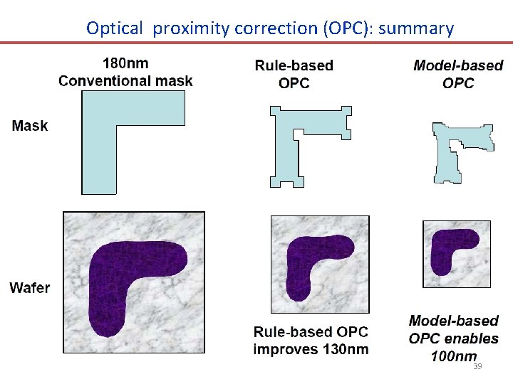
Optical proximity correction (OPC) • Presence or absence of other features nearby (proximity) will affect the optical behavior. • Sharp features are lost because higher spatial frequencies are lost due to diffraction. • These effects can be calculated and can be compensated for. • This improves the resolution by decreasing k 1. Photo-mask Pattern for negative resist Transparent SEM image of photomask with OPC features 35

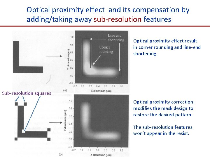
Optical proximity effect and its compensation by adding/taking away sub-resolution features Optical proximity effect result in corner rounding and line-end shortening. Sub-resolution squares Optical proximity correction: modifies the mask design to restore the desired pattern. The sub-resolution features won’t appear in the resist.

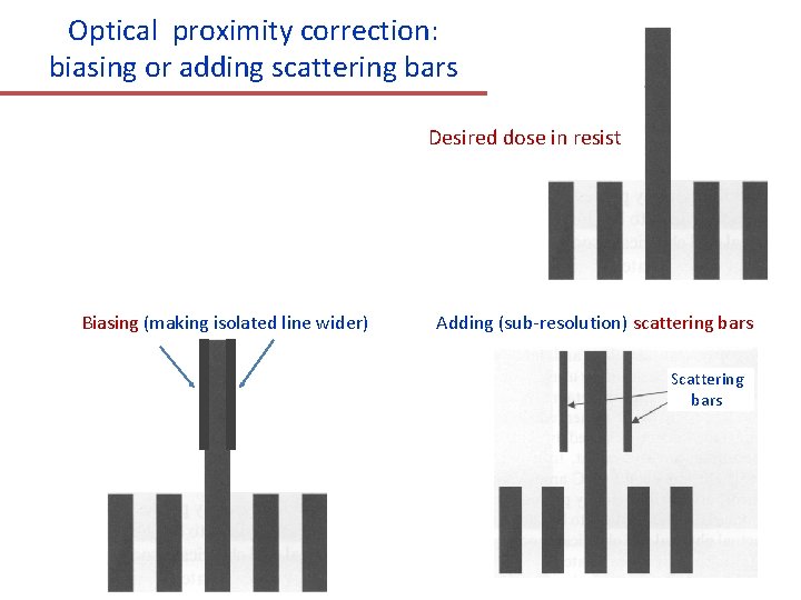
Optical proximity correction: biasing or adding scattering bars Desired dose in resist Biasing (making isolated line wider) Adding (sub-resolution) scattering bars Scattering bars

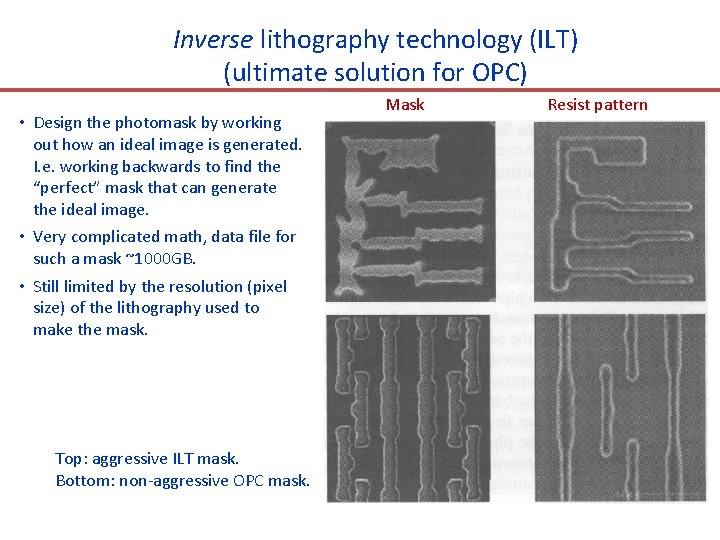
Inverse lithography technology (ILT) (ultimate solution for OPC) • Design the photomask by working out how an ideal image is generated. I. e. working backwards to find the “perfect” mask that can generate the ideal image. • Very complicated math, data file for such a mask ~1000 GB. • Still limited by the resolution (pixel size) of the lithography used to make the mask. Top: aggressive ILT mask. Bottom: non-aggressive OPC mask. Mask Resist pattern

Optical proximity correction (OPC): summary 39

OPC vs PPC (process proximity correction) • Other processes (like etch) also have proximity effect. • Presence or absence of neighbor will affect how a process behaves for a particular feature o Lithography ‘neighborhood’ is about 1 m. o Etch neighborhood is probably few microns (free radical diffusion length). o CMP (chemical mechanical polishing) neighborhood can be few mm. • Correcting for optical (lithography) and few other processes is called process proximity correction (PPC). • Typically lithography + etch corrections are used for PPC. • CMP corrections are at a different (larger) scale: dummy features added to make the feature distribution more even across the wafer. 40

Photolithography and resolution enhancement techniques (RET) 1. 2. 3. 4. 5. 6. Photolithography and resolution limit Immersion lithography Off-axis illumination (OAI) Phase-shift mask (PSM) Optical proximity correction (OPC) Double processing

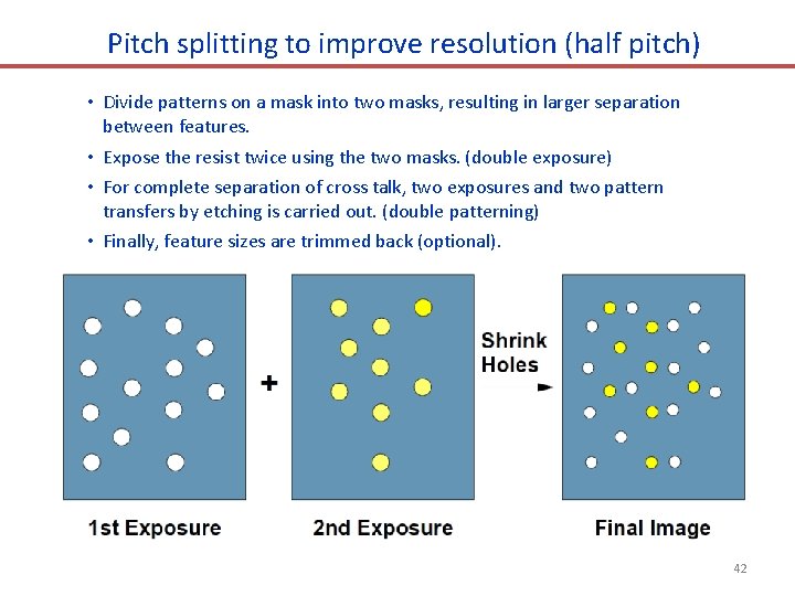
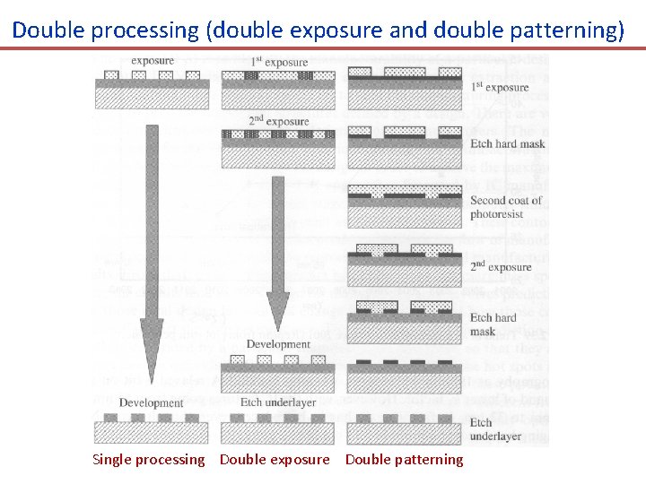
Pitch splitting to improve resolution (half pitch) • Divide patterns on a mask into two masks, resulting in larger separation between features. • Expose the resist twice using the two masks. (double exposure) • For complete separation of cross talk, two exposures and two pattern transfers by etching is carried out. (double patterning) • Finally, feature sizes are trimmed back (optional). 42

Double processing (double exposure and double patterning) Single processing Double exposure Double patterning

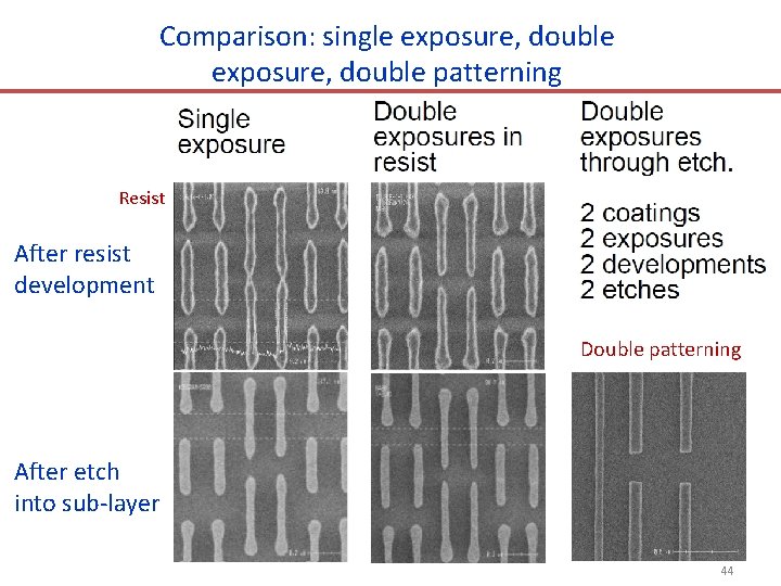
Comparison: single exposure, double patterning Resist After resist development Double patterning After etch into sub-layer 44

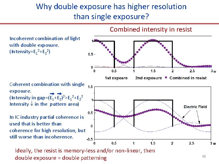
Why double exposure has higher resolution than single exposure? Combined intensity in resist Incoherent combination of light with double exposure. (Intensity=E 12+E 22) Coherent combination with single exposure. (Intensity in gap=(E 1+E 2)2>E 12+E 22 Intensity in the pattern area) In IC industry partial coherence is used that is better than coherence for high resolution, but still worse than incoherence. Ideally, the resist is memory-less and/or non-linear, then double exposure = double patterning 45

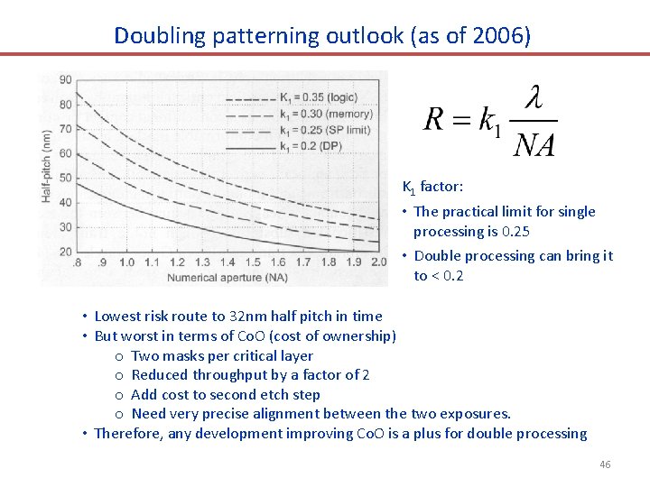
Doubling patterning outlook (as of 2006) K 1 factor: • The practical limit for single processing is 0. 25 • Double processing can bring it to < 0. 2 • Lowest risk route to 32 nm half pitch in time • But worst in terms of Co. O (cost of ownership) o Two masks per critical layer o Reduced throughput by a factor of 2 o Add cost to second etch step o Need very precise alignment between the two exposures. • Therefore, any development improving Co. O is a plus for double processing 46

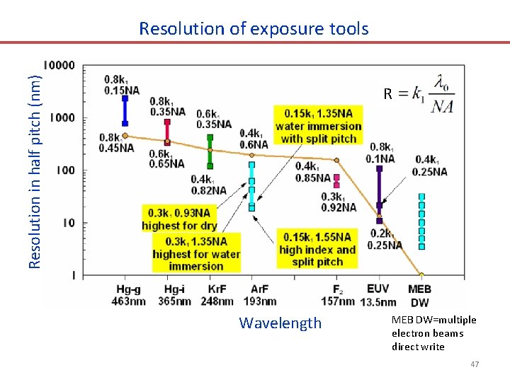
Resolution in half pitch (nm) Resolution of exposure tools R Wavelength MEB DW=multiple electron beams direct write 47