Semiconductor Process Technology What is Semiconductor Process Technology

- Slides: 32

Semiconductor Process Technology

What is Semiconductor Process Technology? q The technology to produce IC microchips q IC chips are the backbone of the computer industry and have spurred related technologies such as software and internet q Every product of the information age is an offspring of IC technology q IC chips increasingly control functions in cars, TVs, VCRs, cameras, mobile phones, toys, etc. q The current technology is as a result of years of research and development, taken many thousands of scientists, engineers and technicians.

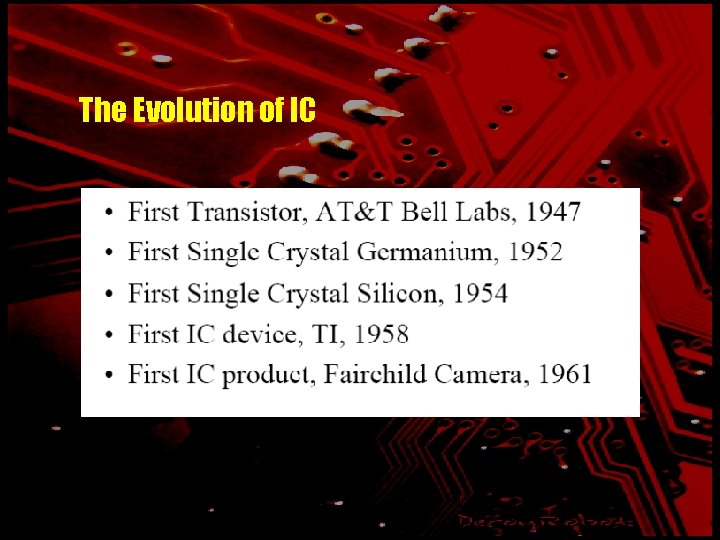
The Evolution of IC

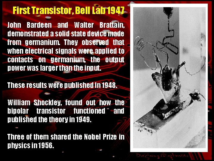
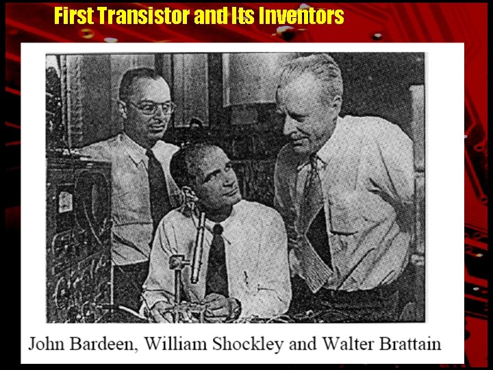
First Transistor, Bell Lab 1947 John Bardeen and Walter Brattain, demonstrated a solid state device made from germanium. They observed that when electrical signals were applied to contacts on germanium, the output power was larger than the input. These results were published In 1948. William Shockley, found out how the bipolar transistor functioned and published theory in 1949. Three of them shared the Nobel Prize in physics in 1956.

First Transistor and Its Inventors

q Semiconductor industry developed rapidly and germanium based transistor quickly replaced vacuum tubes in electronics equipment due to: q smaller size q lower power consumption q lower operating temperature q quicker response time q Single crystal silicon and germanium based devices introduced in 1950 and 1952 respectively (better defect control, hence higher yield).

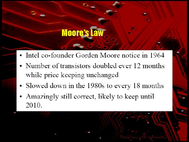
q Shockley left Bell Labs in 1956, to start his own lab in San Francisco Bay, California. Nowadays known as Silicon Valley. His lab has attracted talented scientist such as Robert Noyce and Gordon Moore. q Gordon Moore and Robert Noyce left Shockley in 1957 to start Fairchild Semiconductor.

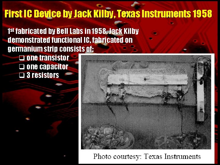
First IC Device by Jack Kilby, Texas Instruments 1958 1 st fabricated by Bell Labs in 1958. Jack Kilby demonstrated functional IC, fabricated on germanium strip consists of; q one transistor q one capacitor q 3 resistors

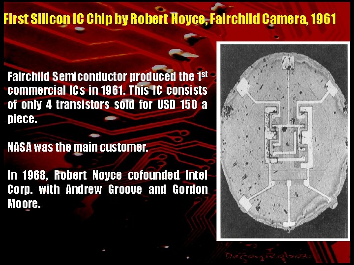
First Silicon IC Chip by Robert Noyce, Fairchild Camera, 1961 Fairchild Semiconductor produced the 1 st commercial ICs in 1961. This IC consists of only 4 transistors sold for USD 150 a piece. NASA was the main customer. In 1968, Robert Noyce cofounded Intel Corp. with Andrew Groove and Gordon Moore.

Moore’s Law

Moore’s Law, Intel Product

IC Integration Scale

Feature Size and Wafer Size

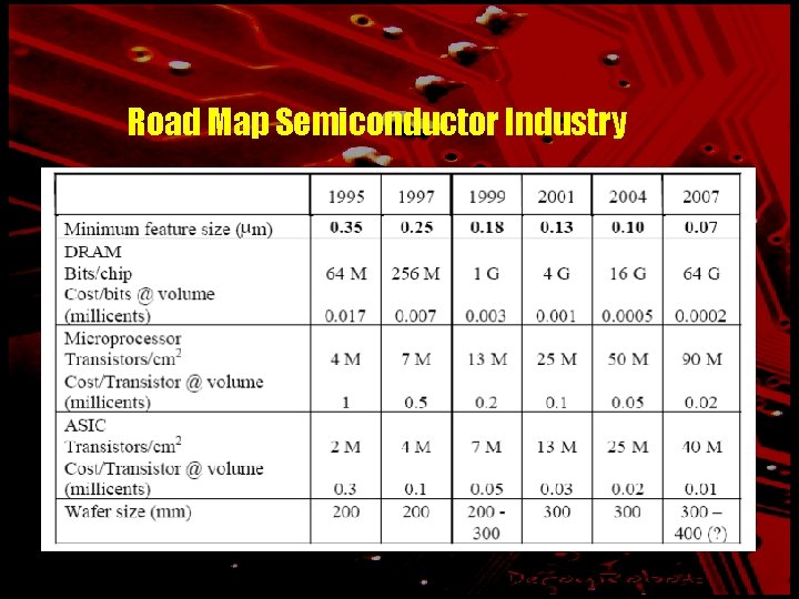
Road Map Semiconductor Industry

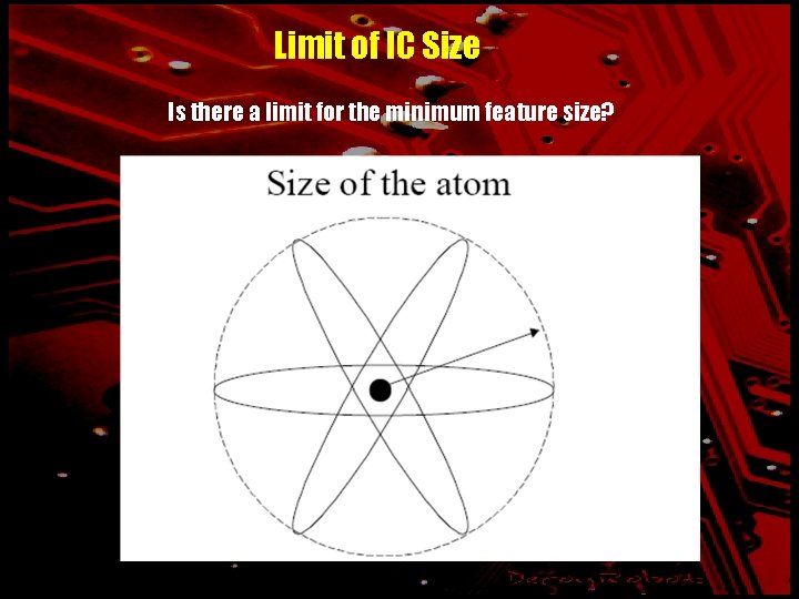
Limit of IC Size Is there a limit for the minimum feature size?

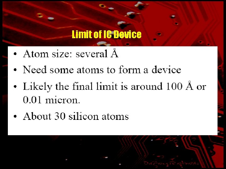
Limit of IC Device

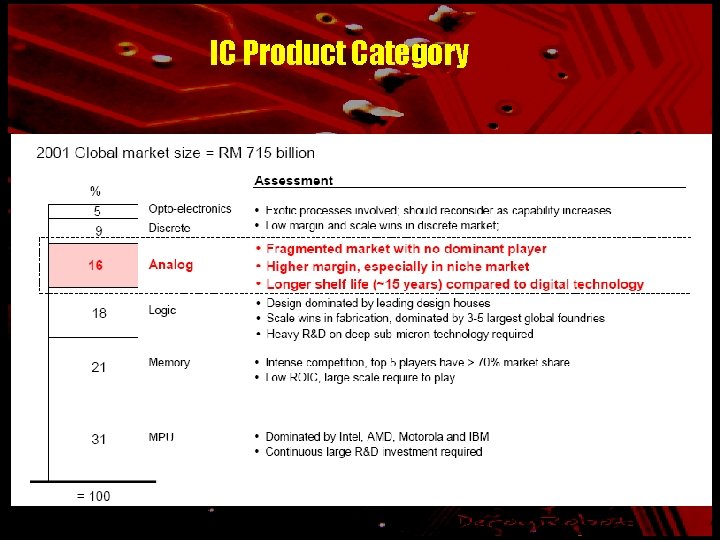
IC Product Category

OVERVIEW ON IC MANUFACTURING

IC Manufacturing q A very complicated process, involves; q Circuit design q Manufacturing material q Clean room technology, processing, equipment q Wafer processing technology q Die testing q Chip packaging and final test

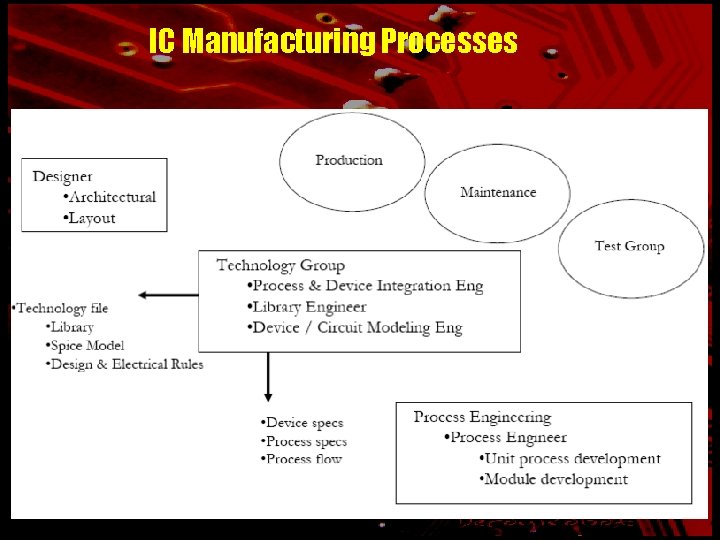
IC Manufacturing Processes

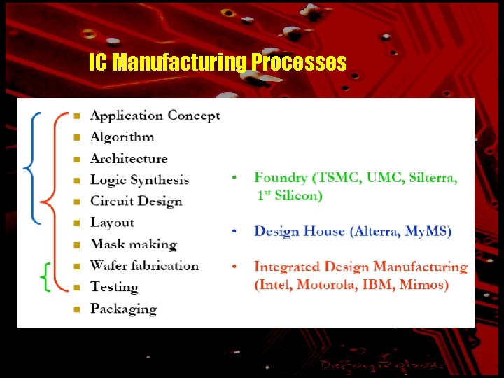
IC Manufacturing Processes

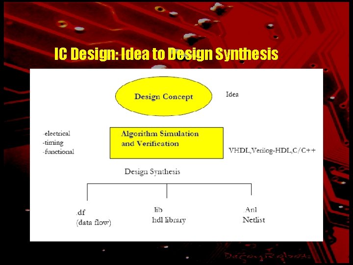
IC Design: Idea to Design Synthesis

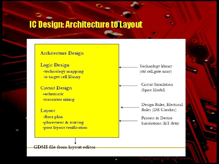
IC Design: Architecture to Layout

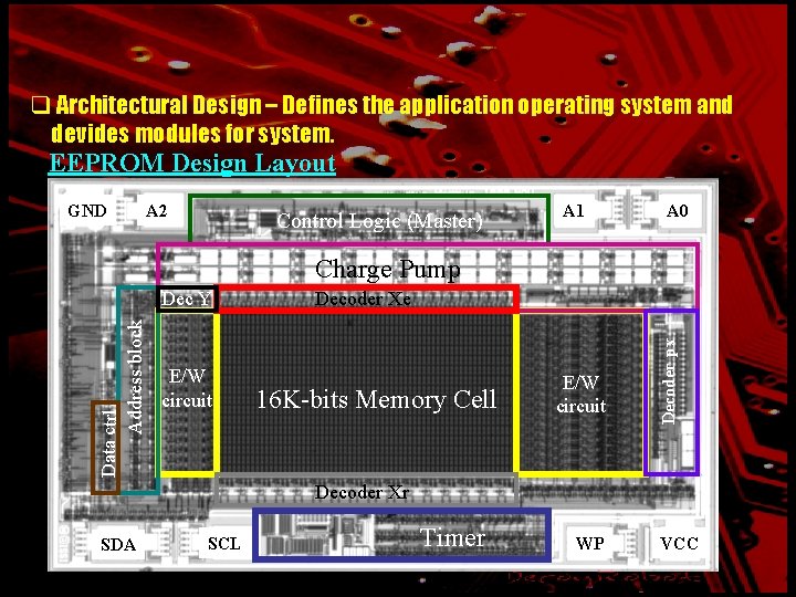
q Architectural Design – Defines the application operating system and devides modules for system. EEPROM Design Layout GND A 2 Control Logic (Master) A 1 A 0 Charge Pump E/W circuit Decoder Xe 16 K-bits Memory Cell E/W circuit Decoder px Data ctrl Address block Dec Y Decoder Xr SDA SCL Timer WP VCC

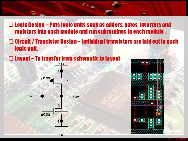
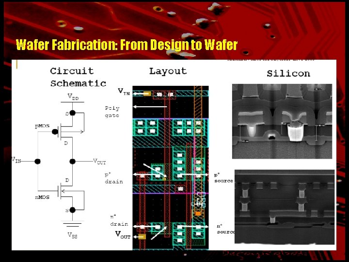
q Logic Design – Puts logic units such as adders, gates, inverters and registers into each module and run subroutines in each module. q Circuit / Transistor Design – Individual transistors are laid out in each logic unit. q Layout – To transfer from schematic to layout VDD S p. MOS D VIN VOUT D n. MOS S VSS

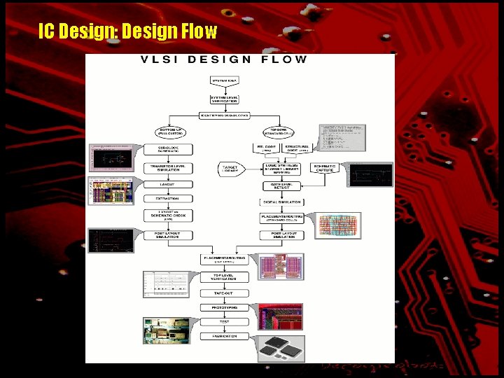
IC Design: Design Flow

Wafer Fabrication: From Design to Wafer

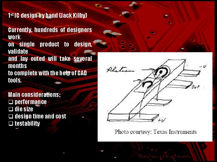
1 st IC design by hand (Jack Kilby) Currently, hundreds of designers work on single product to design, validate and lay outed will take several months to complete with the help of CAD tools. Main considerations; q performance q die size q design time and cost q testability

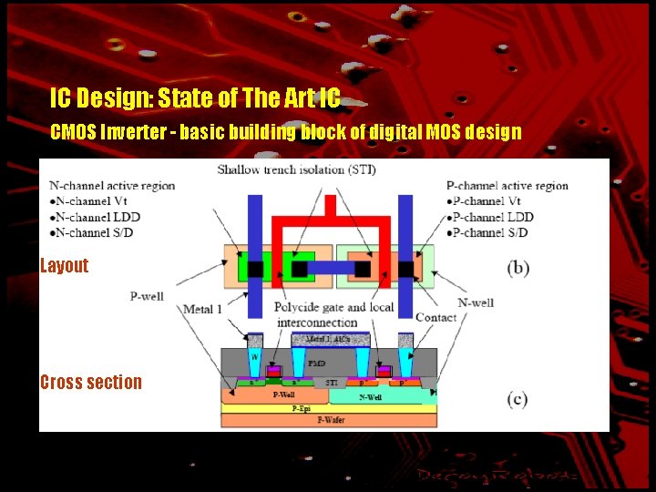
IC Design: State of The Art IC CMOS Inverter - basic building block of digital MOS design Layout Cross section

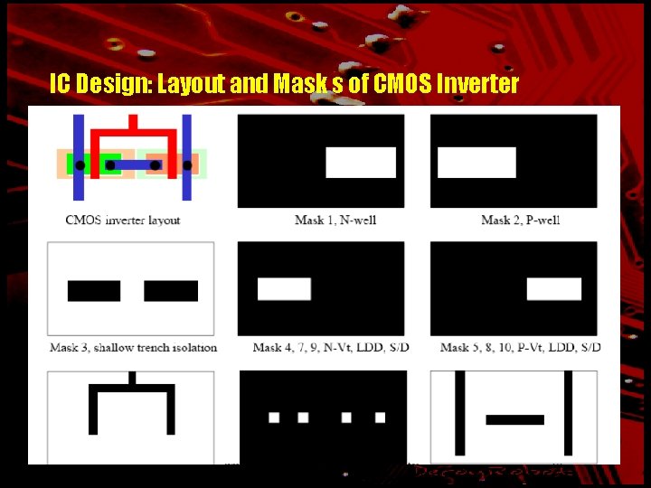
IC Design: Layout and Mask s of CMOS Inverter

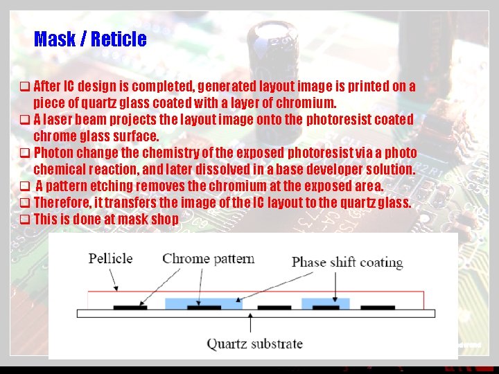
Mask / Reticle q After IC design is completed, generated layout image is printed on a piece of quartz glass coated with a layer of chromium. q A laser beam projects the layout image onto the photoresist coated chrome glass surface. q Photon change the chemistry of the exposed photoresist via a photo chemical reaction, and later dissolved in a base developer solution. q A pattern etching removes the chromium at the exposed area. q Therefore, it transfers the image of the IC layout to the quartz glass. q This is done at mask shop

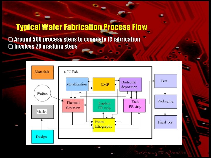
Typical Wafer Fabrication Process Flow q Around 500 process steps to complete IC fabrication q Involves 20 masking steps