Biosensors and Bio MEMS Photolithography soft lithography electron

Biosensors and Bio. MEMS Photolithography, soft lithography, electron beam lithography, Micromachining, metal deposition and bonding Lecturer : Dr Nashrul Fazli Mohd Nasir Contact mask aligner Source: Freescale/ASM SEM
 is originated in United States, The overview of MEMS")
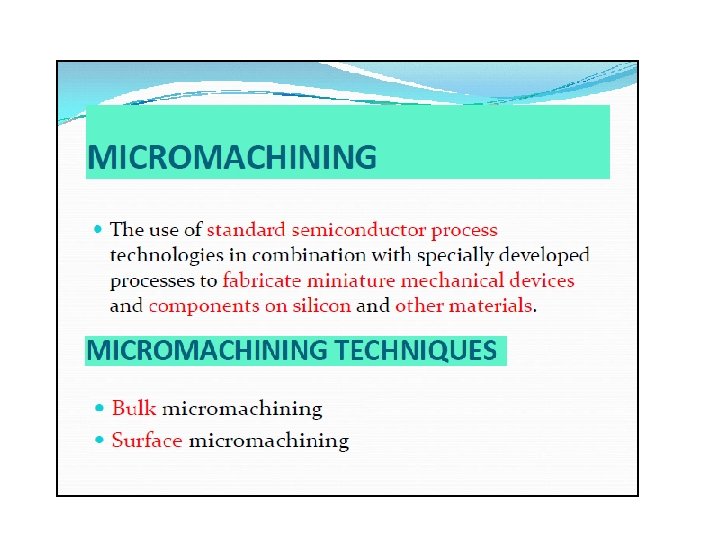
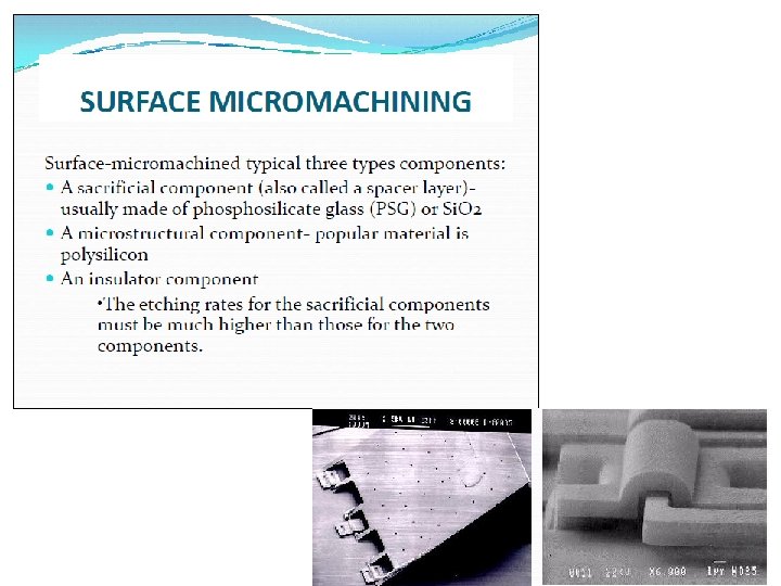
• Micro-electromechanical systems (MEMS) is originated in United States, The overview of MEMS • Referred also as Microsystems Technology (MST) in Europe & Micromachines in Japan. • What is MEMS? • MEMS is a process technology used to create tiny integrated devices or systems that combine mechanical and electrical components. • They are fabricated using integrated circuit (IC) batch processing techniques and can range in size from a few micrometres to millimetres. • These devices (or systems) have the ability to sense, control and actuate on the micro scale, and generate effects on the macro scale.

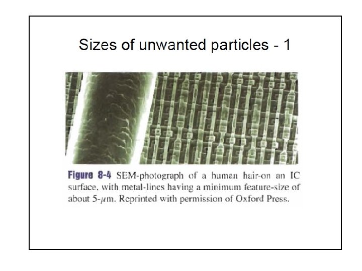
WAFER CLEANING/CLEAN ROOMS

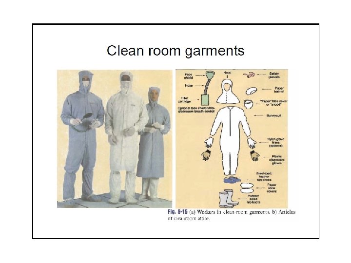
Standard garment wore in a cleanroom

CONTAMINATION EXAMPLE

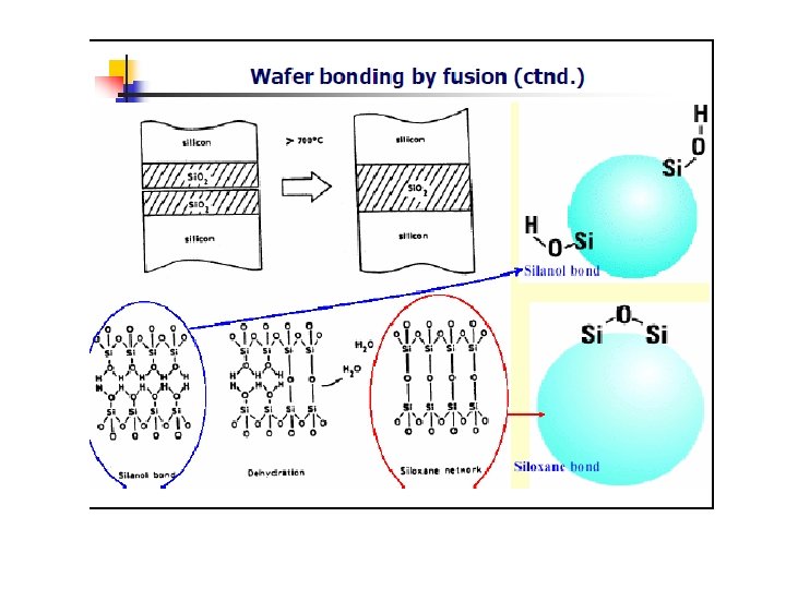
Introduction

Basic Lithography Process Steps • Substrate Clean to prepare surface; prime wafer. • Resist Coat (positive in this example), followed by a bake to remove solvent. Resist Substrate

Basic Lithography Process Steps • Align Photomask to wafer. • Expose pattern through photomask. Light Source/Shutter Photomask Resist Substrate

Basic Lithography Process Steps • Post-Exposure Bake to reduce standing waves and/or to make exposed (Deep Ultra Violet) DUV photoresist soluble in the developer. • Develop away exposed areas and rinse. • Optional hardbake to enhance resistance to chemical or physical attack. • Inspect image and measure overlay and critical dimensions. Resist Substrate

I REPEAT THIS AGAIN!!!!! Basic Steps of Photolithography

Photolithography Process Steps 1. 2. 3. 4. 5. 6. 7. 8. 9. Wafer Cleaning Dehydration Bake HMDS (Hexamethyldisilazane)Priming Photoresist Coating Softbake Align and Expose Photoresist Development Post Exposure Bake Hardbake

Step 1: Dehydration bake • To remove moisture from the wafer surface • Moisture on wafer surface reduces resist adhesion • Wafer on an oxide surface will allow wet etchants to penetrate easily between the resist and the wafer surface • Parameters : Temperature

Step 2: HMDS PRIME • To promote adhesion of the photoresist to the wafer surface • Hexamethyldisilazane • Parameters: • Temperature • Time

Step 3: PHOTORESIST COATING To coat a resist onto the Si wafer for patterning with a required resist thickness and uniformity Parameters : 1. Resist viscosity 2. Resist dispense method 3. Resist dispense velocity 4. Resist dispense volume 5. Resist dispense time 6. Nozzle position 7. Spin speed 8. Spread time 9. Acceleration / deceleration 10. Final spin speed 11. Final spin time 12. Chuck diameter 13. Chuck vacuum 14. Controlled exhaust 15. Ambient atmosphere (RH & Temperature) 16. Cup ambient (RH & Temperature) 17. Wafer centering 18. Machine and chuck leveling 19. Resist temperature control

Photoresist

Photoresist
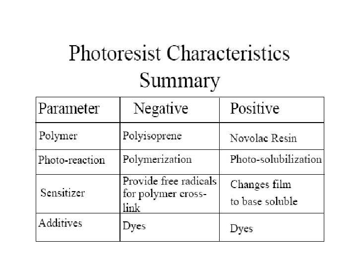

POSITIVE AND NEGATIVE PHOTORESIST

PR Spin Coater Photoresist spread on spinning wafer surface Wafer held on a vacuum chuck Slow spin ~ 500 rpm Ramp up to ~ 3000 - 7000 rpm

Step 4: SOFTBAKE To remove a solvent from photoresist & activates photoactive compound To remove stress in the photoresist To improve photoresist adhesion Parameters 1. Type of heat transfer (Hot plate or convection) 2. Temperature 3. Temperature uniformity 4. Time 5. Exhaust 6. Cool down rate

Step 5: Align and exposure Si wafer with a layer of photoresist on its top will be aligned to the mask and exposed to the UV light.

What is a Photomask? • It provides the master copy of the pattern for the wafer. • The Design layout for the device to be fabricated will typically have many mask patterns. Complex chips may have 50 or so. • The substrate (blank) is made from some form of glass. • There is a chromium layer on one side of the glass that acts as a light barrier. The chrome is selectively removed to form the openings for light. • In many cases the patterns are created using…Lithography!! • Sometimes the mask is called a reticle (see later)

Important Characteristics of Masks • No Defects Permitted • In a reticle (mask with a pellicle, see later), a defect is catastrophic – it will be repeated for every field exposure (chip) on the wafer. • Materials and the line creation process both must be defect-free. • Defect specifications are negotiated with the mask vendor. • High Transmission • The intensity of the light exiting the mask should be nearly equal to the intensity of the light entering it. • Etch resistant • Both the substrate (blank) and light barrier must be resistant to environmental chemical attack. If a mask must be cleaned, the cleaning process must not harm the mask but still remove the contamination. • Low Thermal Expansion • A high thermal expansion leads to registration runout.

Mask Blank Materials • Soda-Lime • Very low cost mask used for large geometries or processes with wide registration specs. Will cause runout of 0. 24 m/°C per inch of substrate diameter during ebeam writing. • Borosilicate • Moderate cost, but seldom used. Has one third of the runout problems. Has less transmission than soda lime. • Quartz • Is the industry standard for high precision registration. Has excellent transmission, even with lower wavelengths (248 nm). Has lower runout by a factor of 20 compared to soda lime. • Fused Silica • Necessary for 248 nm (extended lithography) and 193 nm nodes. Quartz is too birefringent. Like soda lime, Ca. F 2 has too high of a coefficient of thermal expansion.

Light Barrier Material • Chromium – 600 Å to 1000 Å thick, placed on one side of the glass. An antireflective coating of 200 Å is sometimes applied, made of Cr. O 2. • Two sides of mask • Chromium side. The side of the mask facing the wafer • Glass side. The side of the mask facing the light source. Glass Side Chrome Side
 • Why? : contamination on chrome side of")
Pellicle (transparent polymer sheet above mask/reticle) • Why? : contamination on chrome side of wafer. • Pellicle throws contamination out of focus by keeping it several mm away from the chrome side of the mask. Little light is lost through a pellicle. • Made of nitrocellulose or mylar. • Large particles will still cause transmission defects. • Good for projection aligners (scanners, steppers) only. • Frame is mounted to reticle or mask. Pellicle is attached to frame. • Special equipment required. • Pellicles are very susceptible to attack from solvents, even at weak levels in the air. It is expensive and time consuming to replace them. • Pellicles are easily damaged from handling. • Glass side needs no pellicle. The thickness of the glass acts as one. Remember: it is the presence of a particle near the chrome that is costly.

Step 6: POST EXPOSURE BAKE To reduce the effect of standing waves which occur during exposure To increase the resistance of the resist prior to the etching process Parameters : 1. 2. 3. 4. 5. 6. Type of plate (hot plate or convection oven) Temperature uniformity Time Exhaust Cool down rate

Step 8: Development process To remove area of resists that have been exposed/unexposed to form a pattern The development rate for positive resist much less than negative resist Parameters : 1. Development technique (Immersion/Spray/Puddle) 2. Developer type (Metal Ion/metal ion free) 3. Developer concentration 4. Developer temperature 5. Development time 6. Carbon dioxide absorption 7. Agitation 8. Time between exposure and develop 9. Time between develop and rinse 10. Resist thickness 11. Post exposure bake temperature 12. Exposure energy

Development

Developer Solution • Soluble areas of photoresist are dissolved by developer solutions (weak base solution) • Tetramethyl ammonium hydride (TMAH) is commonly used • Visible patterns will appear on the wafer • Quality Measures: • • • Line resolution Uniformity Particles and Defects

Step 9: Hardbake To increase the resistance of the resist To remove any residual solvent Parameters : 1. 2. 3. 4. 5. 6. Type of plate (conduction or convection) Temperature uniformity Time Exhaust Cool down rate Let say, if your pattern doesn’t meet your expectation and you want to remove your photoresist, this step is called STRIPPING. Usually we will use chemical i. e. acetone to remove totally your positive photoresist & methyl ketone for the negative photoresist. Extra Reading Materials : https: //www. ee. washington. edu/research/microtech/cam/PROCESSES/PDF%20 FILES/Photoli thography. pdf http: //www 2. ece. gatech. edu/research/labs/vc/theory/photolith. html
 • Alignment of")
Key Quality Issues of Lithography • Exposure energy dose (under/over development) • Alignment of photolithography mask with features on the wafer • Resolution – smallest feature size available for a given lithography process. • Depth of Focus (DOF) – range of focus settings that provide resolution at the same exposure energy. • Contrast – ability of a resist to • produce acceptably sharp images. Low High
. For a given exposure system – whether")
• Exposure energy dose (under/over development). For a given exposure system – whether the dose is optimum or too much or too little depends on exposure time Desired pattern Over-exposed pattern Under-exposed pattern

• Alignment of photolithography mask with features on the wafer Features on wafer mask wafer alignment marks Features on mask Flat alignment mark Alignment marks used to register two levels. Wafer now ready to be exposed. Mask over wafer

Soft Lithography Techniques • Soft lithography includes several techniques such as: • • Replica Molding (REM) Micro-contact printing (µCP) Micro-transfer molding (µTM) Micro-molding in capillaries (MIMIC)
 • Master mold is replicated in PDMS by casting and curing")
Replica Molding (REM) • Master mold is replicated in PDMS by casting and curing PDMS pre-polymer. • PDMS mold is oxidized in oxygen plasma for 1 minute and exposed to fluorinated silane for 2 hours to make a surface with low adhesion to PDMS. • PDMS is cast against this negative replica, cured and peeled off. • This will make the positive replica of the original master.
 • It uses a PDMS stamp to form patterns of self-assembled")
Micro-Contact Printing (µCP) • It uses a PDMS stamp to form patterns of self-assembled monolayers (SAMs) on the surfaces of substrates. • PDMS stamp is coated with an ink of the molecules and pressed onto the solid surface • Inking creates a Self Assembled Monolayer on the solid surface • the use of elastomers allows the micropatterned surface to come into conformal contact with the surfaces over large areas
 • PDMS stamp is filled with pre polymer • Excess prepolymer")
Micro-Transfer Molding (µTM) • PDMS stamp is filled with pre polymer • Excess prepolymer is removed • Press the rubber stamp against the surface • Cure the polymer • Peel off the stamp
 • Push the PDMS stamp against the substrate. • prepolymer")
Micromolding in Capillaries (MIMIC) • Push the PDMS stamp against the substrate. • prepolymer is applied to access holes in the mold (vacuum assisted). • Prepolymer fills the channels using capillary forces. • Cure the polymer • Peel off the PDMS mold

e-Beam Lithography • Electron source: SEM • Equipment: SEM equipped with a pattern generator and alignment system • e-beam control: – accelerating voltage (k. V) – operation current (p. A) – exposure dose (µC/cm 2) – exposure dwell period (µs)

Steps involved in the EBL process. With a beam current of 600 p. A and an accelerating voltage of 100 k. V, the beam diameter was approximately 3 nm. J. Phys. Chem. B 2002, 106, 11463 -11468

e. BL followed by Self Assembly Langmuir, Vol. 20, No. 9, 2004, 3495

e. BL changes the properties of coating layers Langmuir, Vol. 20, No. 9, 2004 3767
 Backscattered electron (BSE) image of Zn. O patterns on")
Applications of e. BL (a) Backscattered electron (BSE) image of Zn. O patterns on Si. Ox substrates annealed in air at 700 °C for 20 min (b) secondary electron (SE) image before annealing (c) SE image after annealing at 700 °C for 20 min in air (d) SE image of annealed patterns over a large area. Nano Lett. , Vol. 5, No. 9, 2005

Applications of e. BL Proceedings of SPIE Vol. 5184

Anisotropy /ˌænaɪˈsɒtrəpi/ is the property of being directionally dependent, as opposed to isotropy, which implies identical properties in all directions.
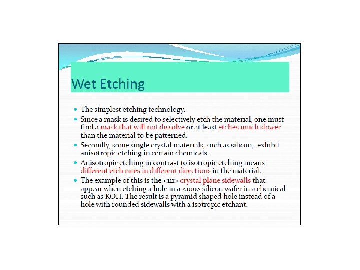

Example of Wet Etching Fig 2. Final product of wet etching

EDP= Ethylene Diamine Pyrochatechol
 Etching • Developed and used for: 1. faster and simpler etching in")
Dry (Plasma) Etching • Developed and used for: 1. faster and simpler etching in a few cases 2. more directional (anisotropic) etching • Both chemical (highly reactive) species and ionic (very directional) species typically play a role.
")
Typical RF-powered plasma etch systems look just like Plasma Enhanced Chemical Vapour Deposition (PECVD) or sputtering systems. Etching gases include halide-containing species such as CF 4, Si. F 6, Cl 2, and HBr, plus additives such as O 2, H 2 and Ar. O 2 by itself is used to etch photoresist. Pressure = 1 m. Torr to 1 Torr. Typically there about 1015 cm-3 neutral species (1 to 10% of which may be free radicals) and 108 -1012 cm-3 ions and electrons.
 is much more directional (e field across")
Physical Etching • Ion etching (below right) is much more directional (e field across plasma) • Etching species are ions like CF 3+ or Ar+ which remove material by sputtering. • Not very selective since all materials sputter at about the same rate. • Physical sputtering can cause damage to surface, with the extent and amount of damage a direct function of ion energy (not ion density).

Ion Enhanced Etching (also known as Deep Reactive Ion Etching, DRIE or the Bosch process) Ion bombardment can enhance etch process (such as by damaging the surface to increase reaction, or by removing etch byproducts i. e. coatings resulting from etching), or can remove inhibitor that is an indirect byproduct of etch process (such as polymer formation from carbon in gas or from photoresist). • Whatever the exact mechanism (multiple mechanisms may occur at same time): need both components for etching to occur. • get anisotropic etching and little undercutting because of directed ion flux. • get selectivity due to chemical component and chemical reactions.

WHAT ARE THE STEPS USED HERE? ? ? ?

Laser Micromachining • Laser micromachining process is a process to create micro size features using laser by removing excess materials • It can be used to cut, drill, & weld the features required during microfabrication • Here, the laser is controlled by switching the laser on & off, controlling the pulse energy & by positioning the substrate or the laser focus • Laser is emitted from the source is passed through the energy attenuator. After it is passed through the beam homogenizer to homogenize the beam. • The target illuminator & machine vision controls the beam to the focusing lens. The lens is moved by precision motion stages. • The beam is then falls on the work piece & the machining takes place.

The laser machine is typically consist of laser, mirrors for beam guide, focusing optic and a positioning system General set up for the laser micromachining equipment

Advantages • Easily automated • Forceless and contactless machining • Minor heat affected zone • Flexibility to design microstructures • High speed and precision • Constant machining quality • No solvent used Disadvantages • Expensive • Need highly skilled operators • Material limitations ( can not be used for reflective materials) • Reflected laser is very hazardous

Thermal Evaporation q In the early years of IC manufacturing, thermal evaporation was widely used for aluminum deposition. q Aluminum is relatively easy to vaporized due to low melting point (6600 C).
 – minimize")
q System needs to be under high vacuum (~ 10 -6 Torr) – minimize residue of oxygen and moisture q Flowing large electric current through aluminum charge – resistive heating. q Aluminum starts to vaporized q When aluminum vapor reaches the wafer surface, it re-condenses and forms a thin aluminum film.

q The deposition rate is mainly related to the heating power, which controlled by the electric current. q The higher the current, the higher the deposition rate. q A significant trace amount of sodium Na, low deposition rate and poor step coverage. q Difficult to precisely control the proper proportions for the alloy films such as Al: Si, Al: Cu and Al: Cu: Si. q No longer used for metallization processes in VLSI and ULSI

Electron Beam Evaporation q A beam of electrons, typically with the energy about 10 ke. V and current up to several amperes, is directed at the metal in a water-cooled crucible in vacuum chamber. q This process heats the metal to the evaporation temperature. q IR lamp is used to heat the wafer (improve step coverage).
 q Less sodium")
q Better step coverage (higher surface mobility due to lamp heating) q Less sodium contamination (only part of aluminum charge is vaporized. q Cannot match the quality of sputtering deposition, therefore very rarely used in advanced semiconductor fab.

Sputtering q The most commonly used PVD process for metallization. q Involves energetic ion bombardment, which physically dislodge atoms or molecules from the solid metal surface, and redeposit them on the substrate as thin metal film. q Argon is normally used as sputtering atom because it is inert, relatively heavy, abundant, cost effective.

Sputtering = ejecting material from a "target" that is a source onto a "substrate" such as a silicon wafer

q When power is applied between two electrodes under low pressure, a free electron is accelerated by the electric field. q When the free electron collides with Ar, another free electron is generated (ionization collision). Ar becomes positively charged. q The free electron repeat this process to generate more free electrons.

q The positively charged Ar ions are accelerated toward a negatively biased cathode, usually called target. q When these energetic argon ions hit the target surface, atoms of the target material are physically removed from the surface by the momentum transfer of the impacting ions and thrown into the vacuum in the form of metal vapor.

q Sputtered-off atoms leave the target and travel inside the vacuum chamber in the form of metal vapor. q Eventually, some of them reach the wafer surface, adsorb and become so-called adatoms. q The adatoms migrate on the surface until they found nucleation sites and rest there. q Other adatoms re-condense around the nucleation sites to form grain. q When the grains grow and meet with other grains, they form a continuous poly-crystalline metal thin film on the wafer surface.

Simple DC Sputtering q The simplest sputtering system. q Wafer is placed on the grounded electrode and the target is the negatively biased electrode, the cathode. q When a high-power DC voltage (several hundred volts) is applied, the argon atoms are ionized by electric field.

q These accelerate and bombard the target, then sputtered-off the target material from the surface.

THANK YOU!
- Slides: 85