Recall Last Lecture The MOSFET has only one


- Slides: 21

Recall Last Lecture • The MOSFET has only one current, ID • Operation of MOSFET – NMOS and PMOS – For NMOS, • VGS > VTN • VDS sat = VGS – VTN – For PMOS • VSG > |VTP| • VSD sat = VSG + VTP © Electronics

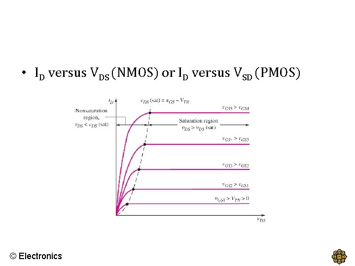
• ID versus VDS (NMOS) or ID versus VSD (PMOS) © Electronics

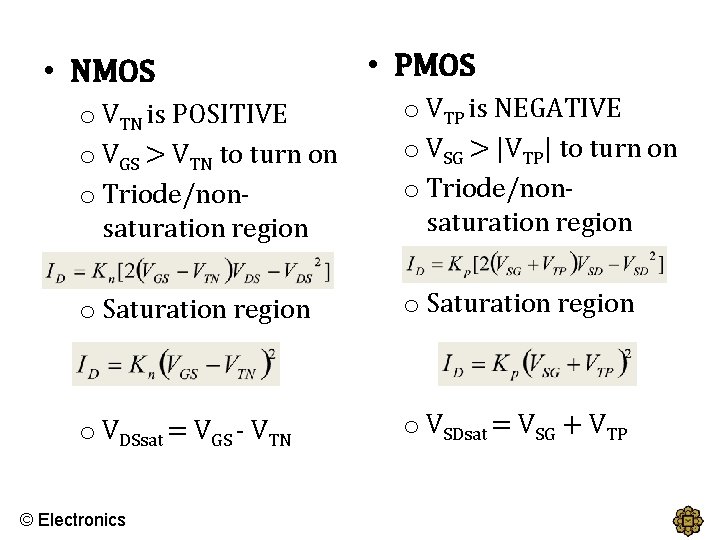
• NMOS • PMOS o VTN is POSITIVE o VGS > VTN to turn on o Triode/nonsaturation region o VTP is NEGATIVE o VSG > |VTP| to turn on o Triode/nonsaturation region o Saturation region o VDSsat = VGS - VTN o VSDsat = VSG + VTP © Electronics

DC analysis of FET © Electronics

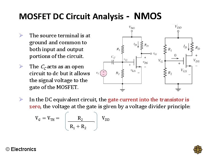
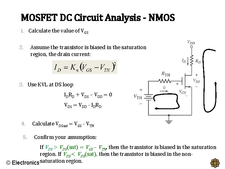
MOSFET DC Circuit Analysis - NMOS Ø The source terminal is at ground and common to both input and output portions of the circuit. Ø The CC acts as an open circuit to dc but it allows the signal voltage to the gate of the MOSFET. Ø In the DC equivalent circuit, the gate current into the transistor is zero, the voltage at the gate is given by a voltage divider principle: VG = VTH = R 2 R 1 + R 2 © Electronics VDD

MOSFET DC Circuit Analysis - NMOS 1. Calculate the value of VGS 2. Assume the transistor is biased in the saturation region, the drain current: 3. Use KVL at DS loop IDRD + VDS – VDD = 0 VDS = VDD - IDRD 4. 5. Calculate VDSsat = VGS - VTN Confirm your assumption: If VDS > VDS(sat) = VGS – VTN, then the transistor is biased in the saturation region. If VDS < VDS(sat), then the transistor is biased in the non© Electronics saturation region.

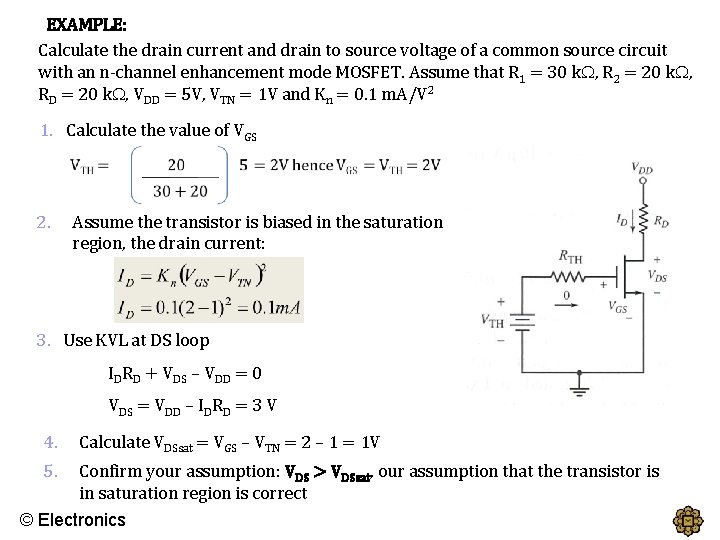
EXAMPLE: Calculate the drain current and drain to source voltage of a common source circuit with an n-channel enhancement mode MOSFET. Assume that R 1 = 30 k , R 2 = 20 k , RD = 20 k , VDD = 5 V, VTN = 1 V and Kn = 0. 1 m. A/V 2 1. Calculate the value of VGS 2. Assume the transistor is biased in the saturation region, the drain current: 3. Use KVL at DS loop IDRD + VDS – VDD = 0 VDS = VDD – IDRD = 3 V 4. 5. Calculate VDSsat = VGS – VTN = 2 – 1 = 1 V Confirm your assumption: VDS > VDSsat, our assumption that the transistor is in saturation region is correct © Electronics

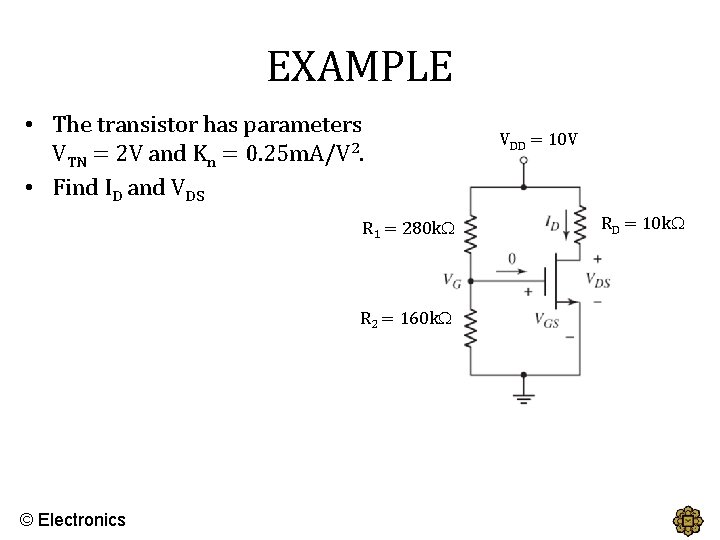
EXAMPLE • The transistor has parameters VTN = 2 V and Kn = 0. 25 m. A/V 2. • Find ID and VDS R 1 = 280 k R 2 = 160 k © Electronics VDD = 10 V RD = 10 k

Solution 1. Calculate the value of VGS KVL at GS loop: VGS – VTH + 0 = 0 VGS = VTH 2. Assume the transistor is biased in the saturation region, the drain current: 3. Use KVL at DS loop IDRD + VDS – VDD = 0 VDS = VDD – IDRD = 3. 31 V 4. Calculate VDSsat = VGS – VTN = 3. 636 – 2 = 1. 636 V 5. Confirm your assumption: VDS > VDSsat, our assumption that the transistor is in saturation region is correct Answer: ID = 0. 669 m. A and VDS = 3. 31 V © Electronics

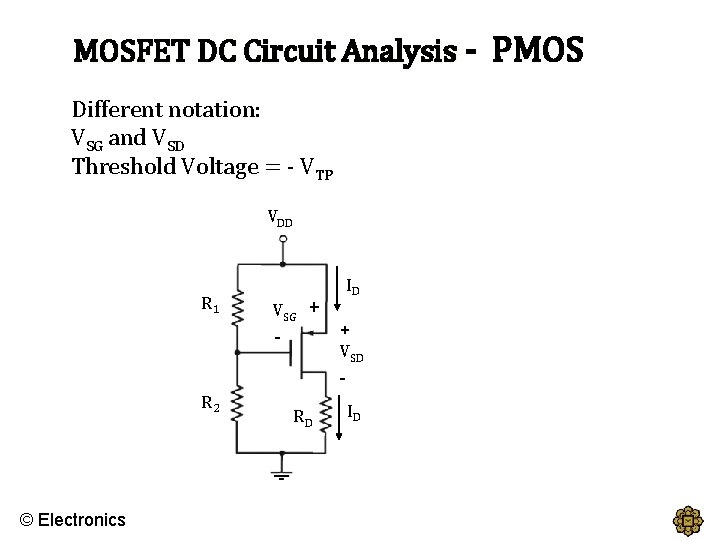
MOSFET DC Circuit Analysis - PMOS Different notation: VSG and VSD Threshold Voltage = - VTP VDD R 1 ID VSG - + + VSD - R 2 © Electronics RD ID

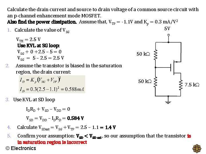
Calculate the drain current and source to drain voltage of a common source circuit with an p-channel enhancement mode MOSFET. Also find the power dissipation. Assume that, VTP = -1. 1 V and Kp = 0. 3 m. A/V 2 5 V 1. Calculate the value of V SG VTH = 2. 5 V Use KVL at SG loop: VSG + 0 +2. 5 – 5 = 0 VSG = 5 – 2. 5 = 2. 5 V 2. 50 k Assume the transistor is biased in the saturation region, the drain current: 50 k 7. 5 k 3. Use KVL at SD loop IDRD + VSD – VDD = 0 VSD = VDD – IDRD = 0. 584 V 4. 5. Calculate VSDsat = VSG +VTP = 2. 5 – 1. 1 = 1. 4 V Confirm your assumption: VSD < VSD sat , so our assumption that the transistor is in saturation region is incorrect © Electronics

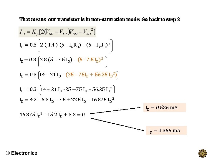
That means our transistor is in non-saturation mode: Go back to step 2 ID = 0. 3 2 ( 1. 4 ) (5 – IDRD) – (5 – IDRD)2 ID = 0. 3 2. 8 (5 – 7. 5 ID) – (5 - 7. 5 ID)2 ID = 0. 3 14 – 21 ID – (25 – 75 ID + 56. 25 ID 2) ID = 0. 3 14 – 21 ID -25 +75 ID – 56. 25 ID 2 ID = 4. 2 – 6. 3 ID – 7. 5 +22. 5 ID – 16. 875 ID 2 ID = 0. 536 m. A 16. 875 ID 2 – 15. 2 ID + 3. 3 = 0 ID = 0. 365 m. A © Electronics

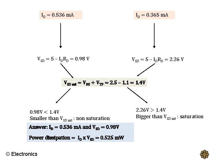
ID = 0. 536 m. A VSD = 5 – IDRD = 0. 98 V ID = 0. 365 m. A VSD = 5 – IDRD = 2. 26 V VSD sat = VSG + VTP = 2. 5 – 1. 1 = 1. 4 V 0. 98 V < 1. 4 V Smaller than VSD sat : non saturation Answer: ID = 0. 536 m. A and VSD = 0. 98 V Power dissipation = ID x VSD = 0. 525 m. W © Electronics 2. 26 V > 1. 4 V Bigger than VSD sat : saturation

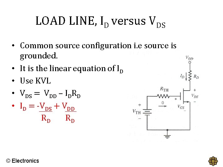
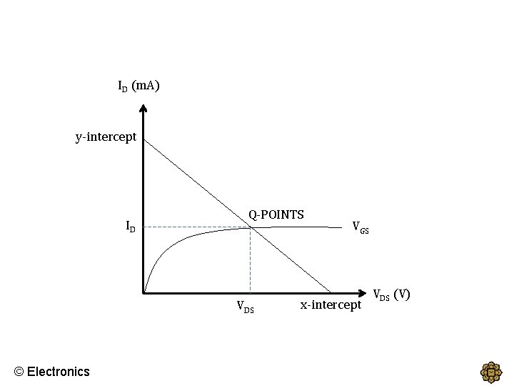
LOAD LINE, ID versus VDS • Common source configuration i. e source is grounded. • It is the linear equation of ID versus VDS • Use KVL • VDS = VDD – IDRD • ID = -VDS + VDD RD RD © Electronics

ID (m. A) y-intercept ID Q-POINTS VDS © Electronics VGS x-intercept VDS (V)

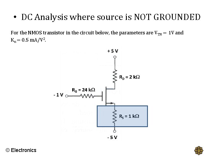
• DC Analysis where source is NOT GROUNDED For the NMOS transistor in the circuit below, the parameters are V TN = 1 V and Kn = 0. 5 m. A/V 2. © Electronics

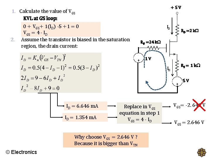
1. Calculate the value of VGS KVL at GS loop: 0 + VGS+ 1(ID) -5 +1 = 0 VGS = 4 - ID 2. Assume the transistor is biased in the saturation region, the drain current: +5 V ID RD =2 k RG =24 k 1 V ID RS = 1 k 5 V ID = 6. 646 m. A ID = 1. 354 m. A Replace in VGS equation in step 1 VGS = 4 - ID Why choose VGS = 2. 646 V ? Because it is bigger than VTN © Electronics VGS= -2. 646 V VGS = 2. 646 V

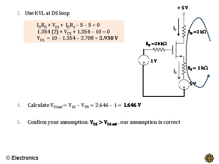
+5 V 3. Use KVL at DS loop IDRD + VDS + IDRS – 5 = 0 1. 354 (2) + VDS + 1. 354 – 10 = 0 VDS = 10 – 1. 354 – 2. 708 = 5. 938 V ID RD =2 k RG =24 k 1 V ID RS = 1 k 5 V 4. Calculate VDSsat = VGS – VTN = 2. 646 – 1 = 1. 646 V 5. Confirm your assumption: VDS > VDS sat , our assumption is correct © Electronics

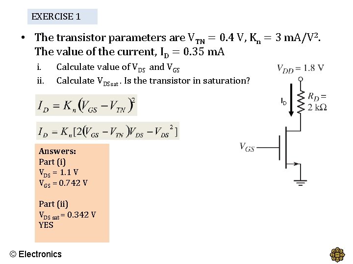
EXERCISE 1 • The transistor parameters are VTN = 0. 4 V, Kn = 3 m. A/V 2. The value of the current, ID = 0. 35 m. A i. ii. Calculate value of VDS and VGS Calculate VDSsat. Is the transistor in saturation? ID Answers: Part (i) VDS = 1. 1 V VGS = 0. 742 V Part (ii) VDS sat = 0. 342 V YES © Electronics

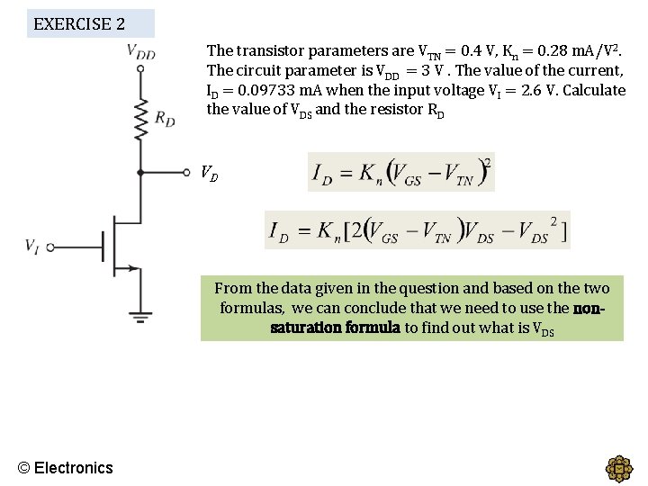
EXERCISE 2 The transistor parameters are VTN = 0. 4 V, Kn = 0. 28 m. A/V 2. The circuit parameter is VDD = 3 V. The value of the current, ID = 0. 09733 m. A when the input voltage VI = 2. 6 V. Calculate the value of VDS and the resistor RD VD From the data given in the question and based on the two formulas, we can conclude that we need to use the nonsaturation formula to find out what is VDS © Electronics

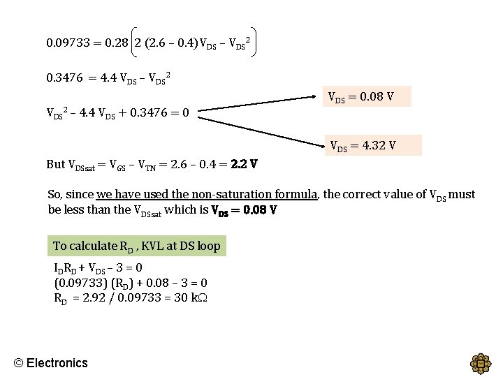
0. 09733 = 0. 28 2 (2. 6 – 0. 4)VDS – VDS 2 0. 3476 = 4. 4 VDS – VDS 2 VDS = 0. 08 V VDS 2 – 4. 4 VDS + 0. 3476 = 0 VDS = 4. 32 V But VDSsat = VGS – VTN = 2. 6 – 0. 4 = 2. 2 V So, since we have used the non-saturation formula, the correct value of VDS must be less than the VDSsat which is VDS = 0. 08 V To calculate RD , KVL at DS loop IDRD + VDS – 3 = 0 (0. 09733) (RD) + 0. 08 – 3 = 0 RD = 2. 92 / 0. 09733 = 30 k © Electronics