Recall Last Lecture The MOSFET has only one

- Slides: 20
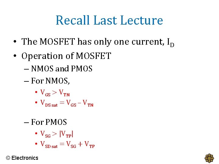
Recall Last Lecture • The MOSFET has only one current, ID • Operation of MOSFET – NMOS and PMOS – For NMOS, • VGS > VTN • VDS sat = VGS – VTN – For PMOS • VSG > |VTP| • VSD sat = VSG + VTP © Electronics
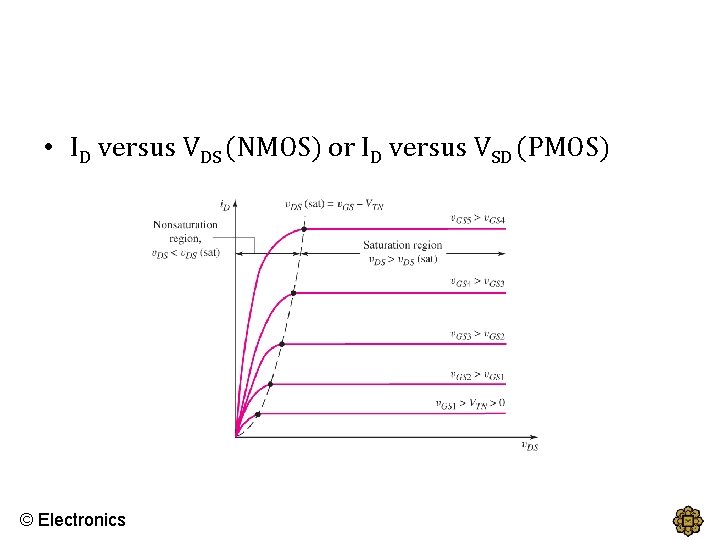
• ID versus VDS (NMOS) or ID versus VSD (PMOS) © Electronics
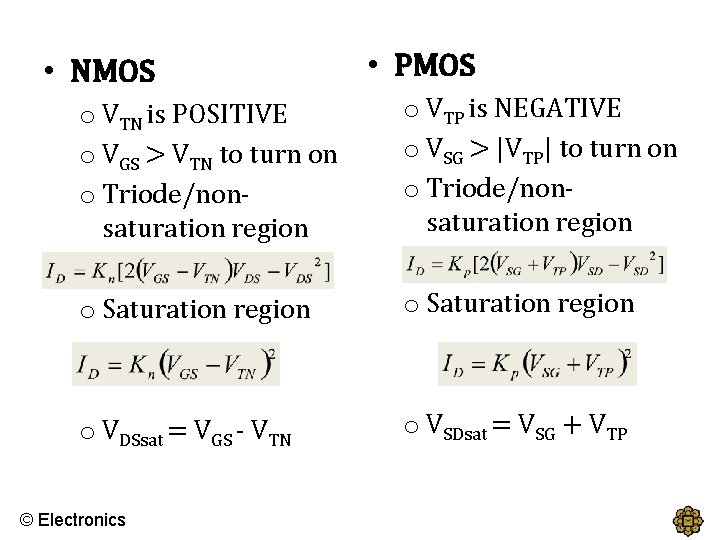
• NMOS • PMOS o VTN is POSITIVE o VGS > VTN to turn on o Triode/nonsaturation region o VTP is NEGATIVE o VSG > |VTP| to turn on o Triode/nonsaturation region o Saturation region o VDSsat = VGS - VTN o VSDsat = VSG + VTP © Electronics
DC analysis of FET © Electronics
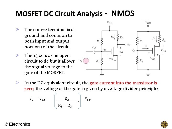
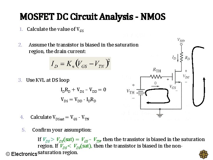
MOSFET DC Circuit Analysis - NMOS Ø The source terminal is at ground and common to both input and output portions of the circuit. Ø The CC acts as an open circuit to dc but it allows the signal voltage to the gate of the MOSFET. Ø In the DC equivalent circuit, the gate current into the transistor is zero, the voltage at the gate is given by a voltage divider principle: VG = VTH = R 2 R 1 + R 2 © Electronics VDD
MOSFET DC Circuit Analysis - NMOS 1. Calculate the value of VGS 2. Assume the transistor is biased in the saturation region, the drain current: 3. Use KVL at DS loop IDRD + VDS – VDD = 0 VDS = VDD - IDRD 4. 5. Calculate VDSsat = VGS - VTN Confirm your assumption: If VDS > VDS(sat) = VGS – VTN, then the transistor is biased in the saturation region. If VDS < VDS(sat), then the transistor is biased in the non© Electronics saturation region.
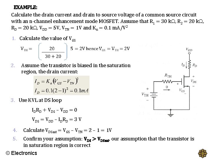
EXAMPLE: Calculate the drain current and drain to source voltage of a common source circuit with an n-channel enhancement mode MOSFET. Assume that R 1 = 30 k , R 2 = 20 k , RD = 20 k , VDD = 5 V, VTN = 1 V and Kn = 0. 1 m. A/V 2 1. Calculate the value of VGS 2. Assume the transistor is biased in the saturation region, the drain current: 3. Use KVL at DS loop IDRD + VDS – VDD = 0 VDS = VDD – IDRD = 3 V 4. 5. Calculate VDSsat = VGS – VTN = 2 – 1 = 1 V Confirm your assumption: VDS > VDSsat, our assumption that the transistor is in saturation region is correct © Electronics
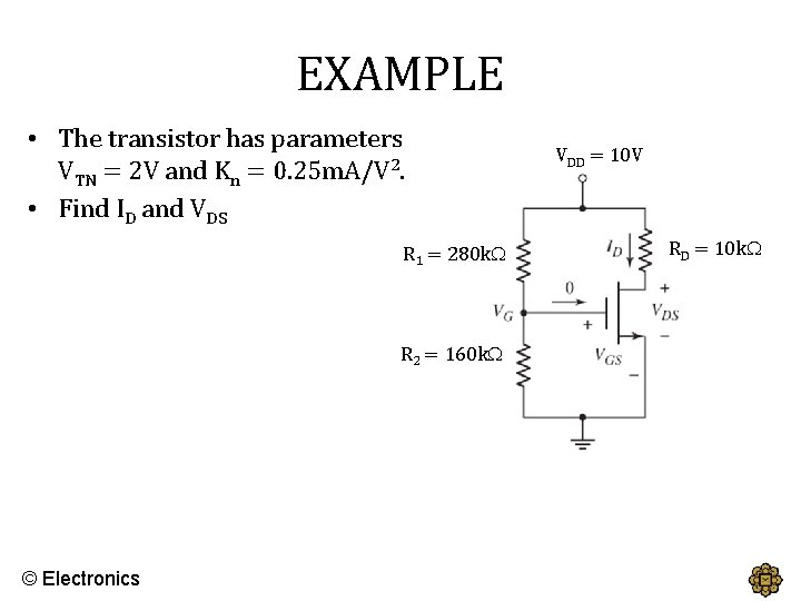
EXAMPLE • The transistor has parameters VTN = 2 V and Kn = 0. 25 m. A/V 2. • Find ID and VDS R 1 = 280 k R 2 = 160 k © Electronics VDD = 10 V RD = 10 k
Solution 1. Calculate the value of VGS KVL at GS loop: VGS – VTH + 0 = 0 VGS = VTH 2. Assume the transistor is biased in the saturation region, the drain current: 3. Use KVL at DS loop IDRD + VDS – VDD = 0 VDS = VDD – IDRD = 3. 31 V 4. Calculate VDSsat = VGS – VTN = 3. 636 – 2 = 1. 636 V 5. Confirm your assumption: VDS > VDSsat, our assumption that the transistor is in saturation region is correct Answer: ID = 0. 669 m. A and VDS = 3. 31 V © Electronics
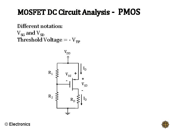
MOSFET DC Circuit Analysis - PMOS Different notation: VSG and VSD Threshold Voltage = - VTP VDD R 1 ID VSG - + + VSD - R 2 © Electronics RD ID
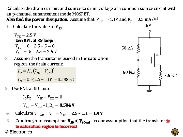
Calculate the drain current and source to drain voltage of a common source circuit with an p-channel enhancement mode MOSFET. Also find the power dissipation. Assume that, VTP = -1. 1 V and Kp = 0. 3 m. A/V 2 5 V 1. Calculate the value of V SG VTH = 2. 5 V Use KVL at SG loop: VSG + 0 +2. 5 – 5 = 0 VSG = 5 – 2. 5 = 2. 5 V 2. 50 k Assume the transistor is biased in the saturation region, the drain current: 50 k 7. 5 k 3. Use KVL at SD loop IDRD + VSD – VDD = 0 VSD = VDD – IDRD = 0. 584 V 4. 5. Calculate VSDsat = VSG +VTP = 2. 5 – 1. 1 = 1. 4 V Confirm your assumption: VSD < VSD sat , so our assumption that the transistor is in saturation region is incorrect © Electronics
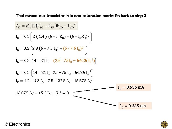
That means our transistor is in non-saturation mode: Go back to step 2 ID = 0. 3 2 ( 1. 4 ) (5 – IDRD) – (5 – IDRD)2 ID = 0. 3 2. 8 (5 – 7. 5 ID) – (5 - 7. 5 ID)2 ID = 0. 3 14 – 21 ID – (25 – 75 ID + 56. 25 ID 2) ID = 0. 3 14 – 21 ID -25 +75 ID – 56. 25 ID 2 ID = 4. 2 – 6. 3 ID – 7. 5 +22. 5 ID – 16. 875 ID 2 ID = 0. 536 m. A 16. 875 ID 2 – 15. 2 ID + 3. 3 = 0 ID = 0. 365 m. A © Electronics
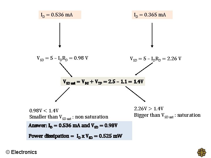
ID = 0. 536 m. A VSD = 5 – IDRD = 0. 98 V ID = 0. 365 m. A VSD = 5 – IDRD = 2. 26 V VSD sat = VSG + VTP = 2. 5 – 1. 1 = 1. 4 V 0. 98 V < 1. 4 V Smaller than VSD sat : non saturation Answer: ID = 0. 536 m. A and VSD = 0. 98 V Power dissipation = ID x VSD = 0. 525 m. W © Electronics 2. 26 V > 1. 4 V Bigger than VSD sat : saturation
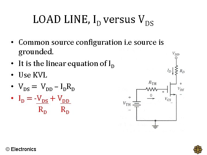
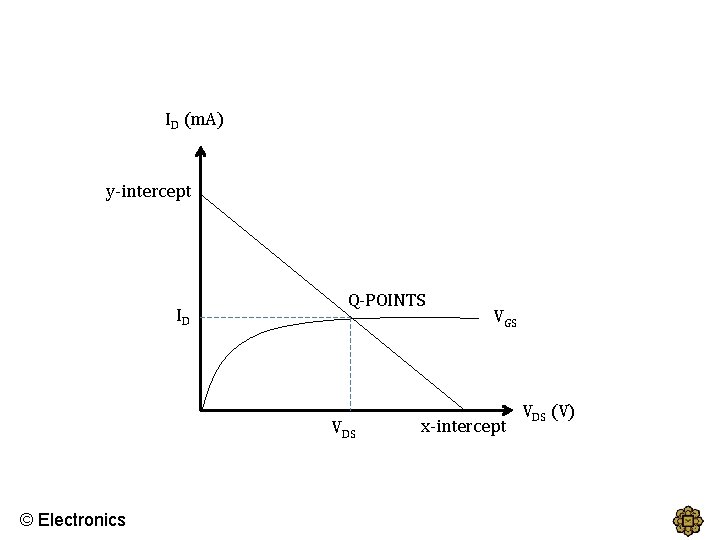
LOAD LINE, ID versus VDS • Common source configuration i. e source is grounded. • It is the linear equation of ID versus VDS • Use KVL • VDS = VDD – IDRD • ID = -VDS + VDD RD RD © Electronics
ID (m. A) y-intercept ID Q-POINTS VDS © Electronics VGS x-intercept VDS (V)
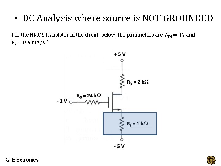
• DC Analysis where source is NOT GROUNDED For the NMOS transistor in the circuit below, the parameters are V TN = 1 V and Kn = 0. 5 m. A/V 2. © Electronics
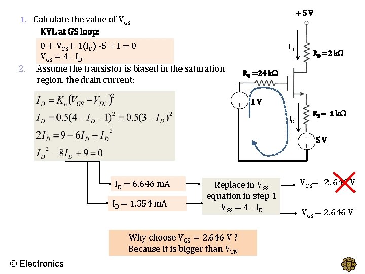
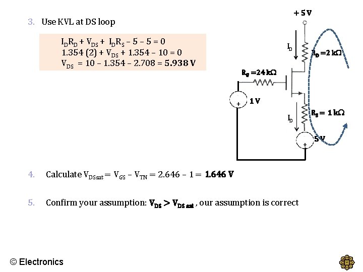
1. Calculate the value of VGS KVL at GS loop: 0 + VGS+ 1(ID) -5 +1 = 0 VGS = 4 - ID 2. Assume the transistor is biased in the saturation region, the drain current: +5 V ID RD =2 k RG =24 k 1 V ID RS = 1 k 5 V ID = 6. 646 m. A ID = 1. 354 m. A Replace in VGS equation in step 1 VGS = 4 - ID Why choose VGS = 2. 646 V ? Because it is bigger than VTN © Electronics VGS= -2. 646 V VGS = 2. 646 V
+5 V 3. Use KVL at DS loop IDRD + VDS + IDRS – 5 = 0 1. 354 (2) + VDS + 1. 354 – 10 = 0 VDS = 10 – 1. 354 – 2. 708 = 5. 938 V ID RD =2 k RG =24 k 1 V ID RS = 1 k 5 V 4. Calculate VDSsat = VGS – VTN = 2. 646 – 1 = 1. 646 V 5. Confirm your assumption: VDS > VDS sat , our assumption is correct © Electronics
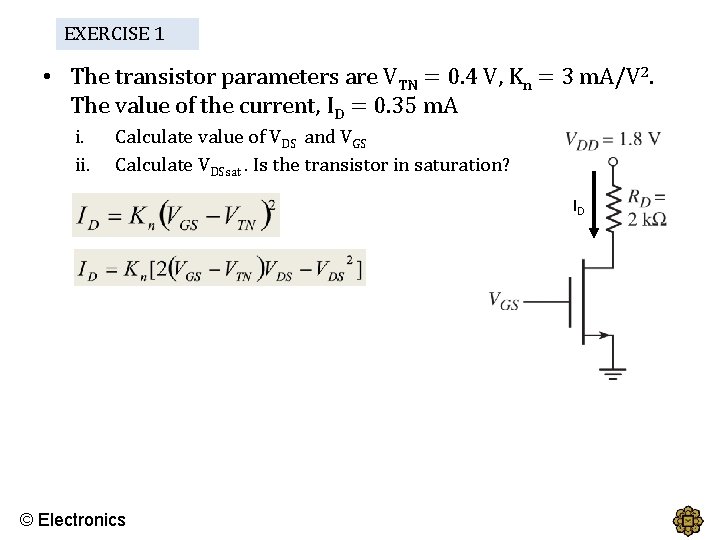
EXERCISE 1 • The transistor parameters are VTN = 0. 4 V, Kn = 3 m. A/V 2. The value of the current, ID = 0. 35 m. A i. ii. Calculate value of VDS and VGS Calculate VDSsat. Is the transistor in saturation? ID Answers: Part (i) VDS = 1. 1 V VGS = 0. 742 V Part (ii) VDS sat = 0. 342 V YES © Electronics
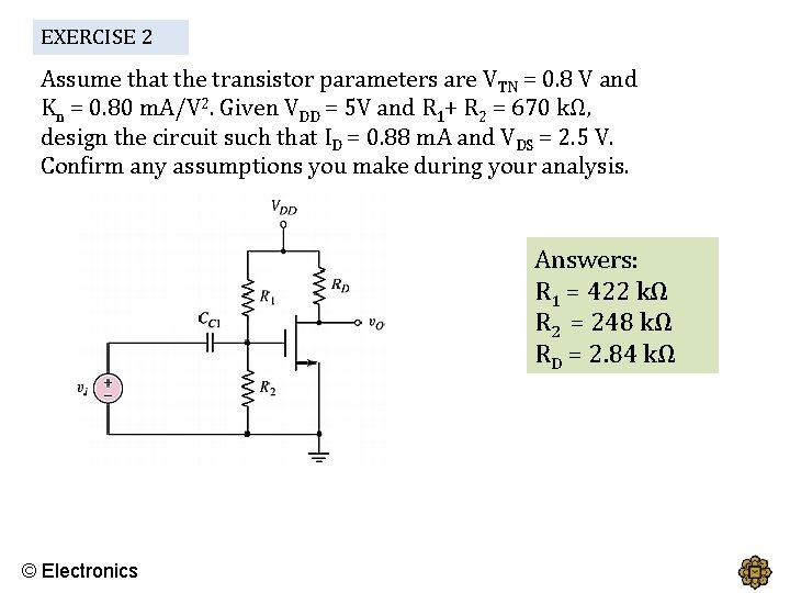
EXERCISE 2 Assume that the transistor parameters are VTN = 0. 8 V and Kn = 0. 80 m. A/V 2. Given VDD = 5 V and R 1+ R 2 = 670 kΩ, design the circuit such that ID = 0. 88 m. A and VDS = 2. 5 V. Confirm any assumptions you make during your analysis. Answers: R 1 = 422 kΩ R 2 = 248 kΩ RD = 2. 84 kΩ © Electronics