PSU Erie Computational Materials Science Properties of Point
![PSU – Erie Computational Materials Science 2001 Convergence: Basis size DE [e. V] • PSU – Erie Computational Materials Science 2001 Convergence: Basis size DE [e. V] •](https://slidetodoc.com/presentation_image/ab9be3cc92710ef741ce31ee55fb5d8a/image-18.jpg)
![PSU – Erie Computational Materials Science 2001 • [D] concentration thermally activated with Ed PSU – Erie Computational Materials Science 2001 • [D] concentration thermally activated with Ed](https://slidetodoc.com/presentation_image/ab9be3cc92710ef741ce31ee55fb5d8a/image-40.jpg)
- Slides: 52

PSU – Erie Computational Materials Science Properties of Point Defects in Semiconductors Dr. Blair R. Tuttle Assistant Professor of Physics Penn State University at Erie, The Behrend College © Blair Tuttle 2001

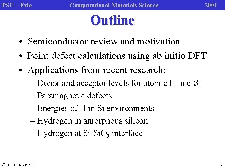
PSU – Erie Computational Materials Science 2001 Outline • Semiconductor review and motivation • Point defect calculations using ab initio DFT • Applications from recent research: – Donor and acceptor levels for atomic H in c-Si – Paramagnetic defects – Energies of H in Si environments – Hydrogen in amorphous silicon – Hydrogen at Si-Si. O 2 interface © Blair Tuttle 2001 2

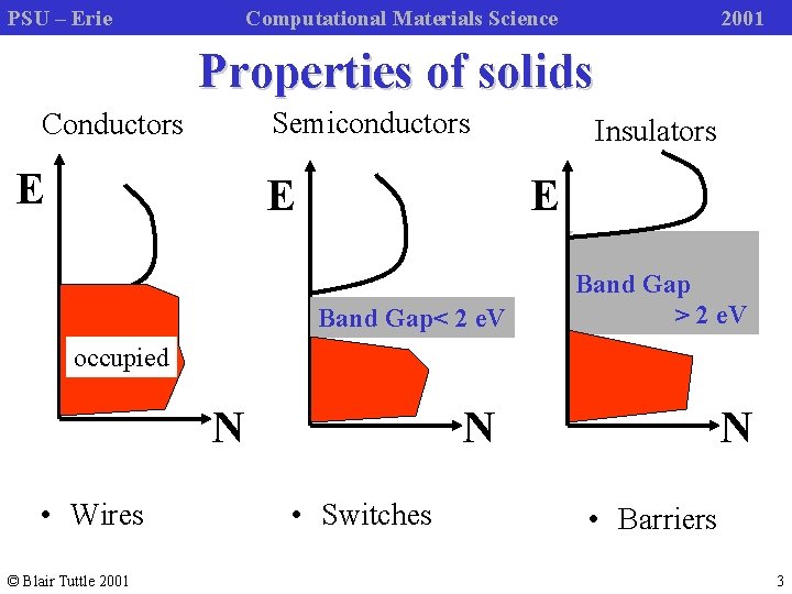
PSU – Erie Computational Materials Science 2001 Properties of solids Semiconductors Conductors E E Insulators E Band Gap< 2 e. V Band Gap > 2 e. V occupied N • Wires © Blair Tuttle 2001 N • Switches N • Barriers 3

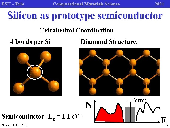
PSU – Erie Computational Materials Science 2001 Silicon as prototype semiconductor Tetrahedral Coordination 4 bonds per Si Diamond Structure: N Semiconductor: Eg = 1. 1 e. V : © Blair Tuttle 2001 E-Fermi E 4

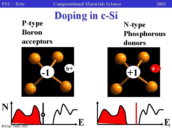
PSU – Erie Computational Materials Science P-type Boron acceptors -1 Doping in c-Si h+ 2001 N-type Phosphorous donors +1 e- N © Blair Tuttle 2001 E E 5

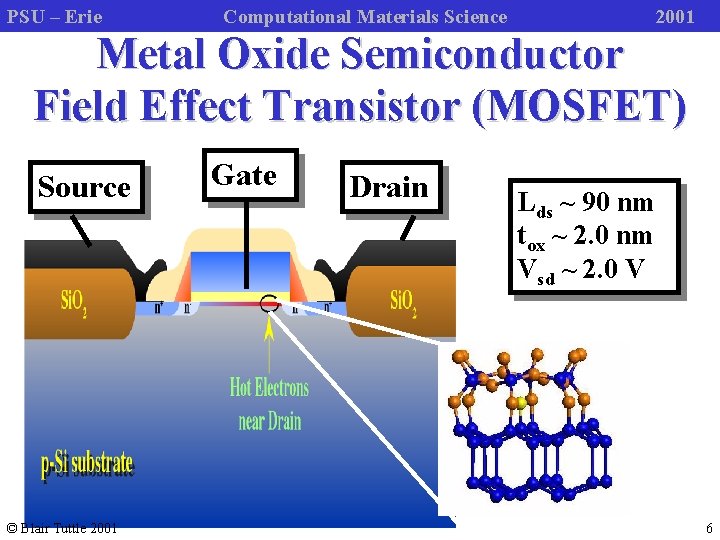
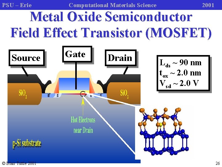
PSU – Erie Computational Materials Science 2001 Metal Oxide Semiconductor Field Effect Transistor (MOSFET) Source © Blair Tuttle 2001 Gate Drain Lds ~ 90 nm tox ~ 2. 0 nm Vsd ~ 2. 0 V 6

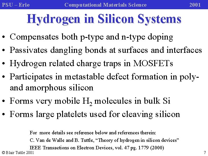
PSU – Erie Computational Materials Science 2001 Hydrogen in Silicon Systems • • Compensates both p-type and n-type doping Passivates dangling bonds at surfaces and interfaces Hydrogen related charge traps in MOSFETs Participates in metastable defect formation in polyand amorphous silicon • Forms very mobile H 2 molecules in bulk Si • Forms large platelets used for cleaving silicon For more details see reference below and references therein: C. Van de Walle and B. Tuttle, “Theory of hydrogen in silicon devices” IEEE Transactions on Electron Devices, vol. 47 pg. 1779 (2000) © Blair Tuttle 2001 7

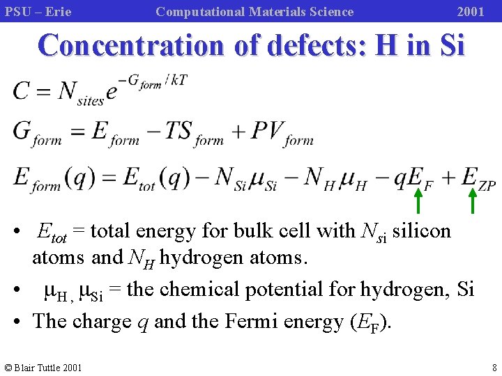
PSU – Erie Computational Materials Science 2001 Concentration of defects: H in Si • Etot = total energy for bulk cell with Nsi silicon atoms and NH hydrogen atoms. • m. H , m. Si = the chemical potential for hydrogen, Si • The charge q and the Fermi energy (EF). © Blair Tuttle 2001 8

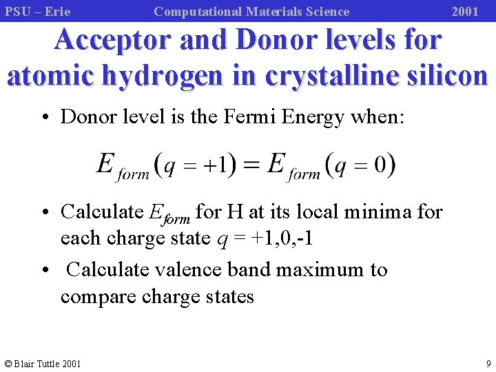
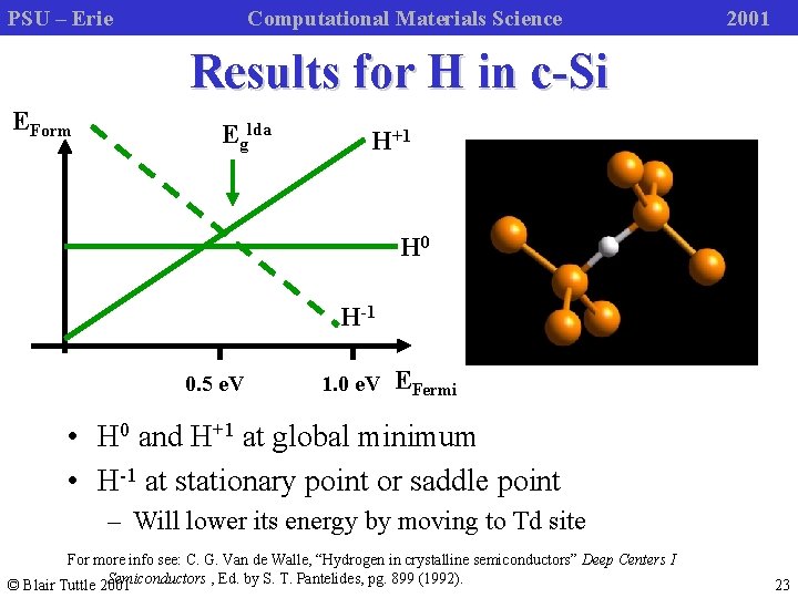
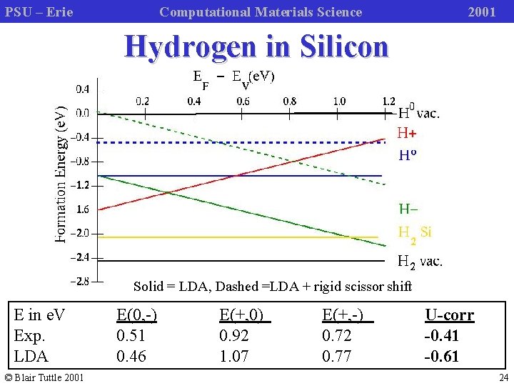
PSU – Erie Computational Materials Science 2001 Acceptor and Donor levels for atomic hydrogen in crystalline silicon • Donor level is the Fermi Energy when: • Calculate Eform for H at its local minima for each charge state q = +1, 0, -1 • Calculate valence band maximum to compare charge states © Blair Tuttle 2001 9

PSU – Erie Computational Materials Science 2001 Choose Method • Semi-empirical – Tight binding (TB) – Classical Potentials • Ab intio – Quantum Monte Carlo (QMC) – Hartree-Fock methods (HF) – Density Function Theory (DFT) For more details on a state-of-the-art implimentation of DFT: Kresse and Furthmuller, ”Efficient iterative schemes for ab intio total-energy calculations using a plane wave basis set” Phys. Rev. B vol. 54 pg. 11169 (1996). http: //cms. mpi. univie. ac. at/vasp/vasp. html © Blair Tuttle 2001 10

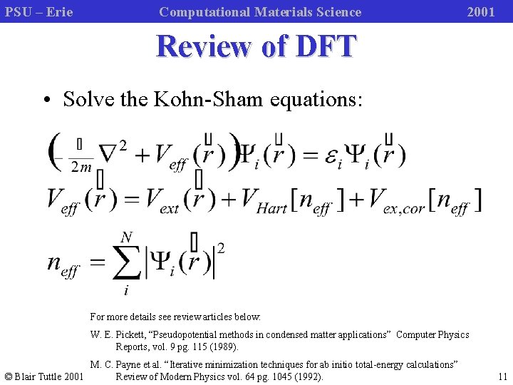
PSU – Erie Computational Materials Science 2001 Review of DFT • Solve the Kohn-Sham equations: For more details see review articles below: W. E. Pickett, “Pseudopotential methods in condensed matter applications” Computer Physics Reports, vol. 9 pg. 115 (1989). M. C. Payne et al. “Iterative minimization techniques for ab initio total-energy calculations” © Blair Tuttle 2001 Review of Modern Physics vol. 64 pg. 1045 (1992). 11

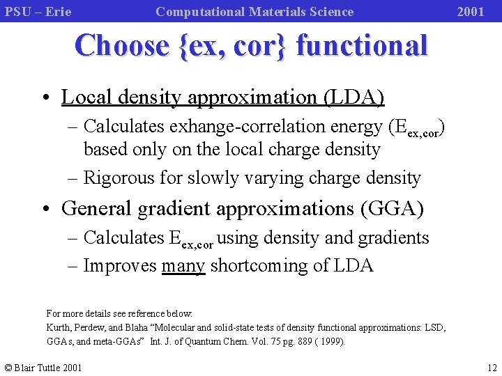
PSU – Erie Computational Materials Science 2001 Choose {ex, cor} functional • Local density approximation (LDA) – Calculates exhange-correlation energy (Eex, cor) based only on the local charge density – Rigorous for slowly varying charge density • General gradient approximations (GGA) – Calculates Eex, cor using density and gradients – Improves many shortcoming of LDA For more details see reference below: Kurth, Perdew, and Blaha “Molecular and solid-state tests of density functional approximations: LSD, GGAs, and meta-GGAs” Int. J. of Quantum Chem. Vol. 75 pg. 889 ( 1999). © Blair Tuttle 2001 12

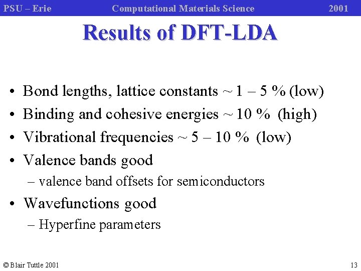
PSU – Erie Computational Materials Science 2001 Results of DFT-LDA • • Bond lengths, lattice constants ~ 1 – 5 % (low) Binding and cohesive energies ~ 10 % (high) Vibrational frequencies ~ 5 – 10 % (low) Valence bands good – valence band offsets for semiconductors • Wavefunctions good – Hyperfine parameters © Blair Tuttle 2001 13

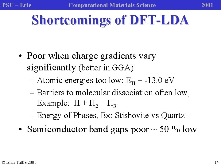
PSU – Erie Computational Materials Science 2001 Shortcomings of DFT-LDA • Poor when charge gradients vary significantly (better in GGA) – Atomic energies too low: EH = -13. 0 e. V – Barriers to molecular dissociation often low, Example: H + H 2 = H 3 – Energy of Phases, Ex: Stishovite vs Quartz • Semiconductor band gaps poor ~ 50 % low © Blair Tuttle 2001 14

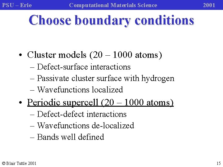
PSU – Erie Computational Materials Science 2001 Choose boundary conditions • Cluster models (20 – 1000 atoms) – Defect-surface interactions – Passivate cluster surface with hydrogen – Wavefunctions localized • Periodic supercell (20 – 1000 atoms) – Defect-defect interactions – Wavefunctions de-localized – Bands well defined © Blair Tuttle 2001 15

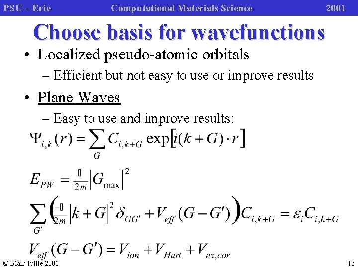
PSU – Erie Computational Materials Science 2001 Choose basis for wavefunctions • Localized pseudo-atomic orbitals – Efficient but not easy to use or improve results • Plane Waves – Easy to use and improve results: © Blair Tuttle 2001 16

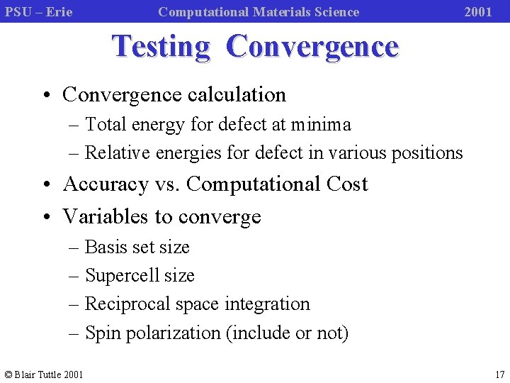
PSU – Erie Computational Materials Science 2001 Testing Convergence • Convergence calculation – Total energy for defect at minima – Relative energies for defect in various positions • Accuracy vs. Computational Cost • Variables to converge – Basis set size – Supercell size – Reciprocal space integration – Spin polarization (include or not) © Blair Tuttle 2001 17
![PSU Erie Computational Materials Science 2001 Convergence Basis size DE e V PSU – Erie Computational Materials Science 2001 Convergence: Basis size DE [e. V] •](https://slidetodoc.com/presentation_image/ab9be3cc92710ef741ce31ee55fb5d8a/image-18.jpg)
PSU – Erie Computational Materials Science 2001 Convergence: Basis size DE [e. V] • Plane waves are a complete basis so crank up the G vectors until convergence is reached. © Blair Tuttle 2001 EPW [Ryd. ] 18

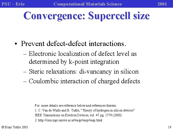
PSU – Erie Computational Materials Science 2001 Convergence: Supercell size • Prevent defect-defect interactions. – Electronic localization of defect level as determined by k-point integration – Steric relaxations: di-vancancy in silicon – Coulombic interaction of charged defects For more details see reference below and references therein: 1. C. Van de Walle and B. Tuttle, “Theory of hydrogen in silicon devices” IEEE Transactions on Electron Devices, vol. 47 pg. 1779 (2000) 2. http: //cms. mpi. univie. ac. at/vasp/vasp. html © Blair Tuttle 2001 19

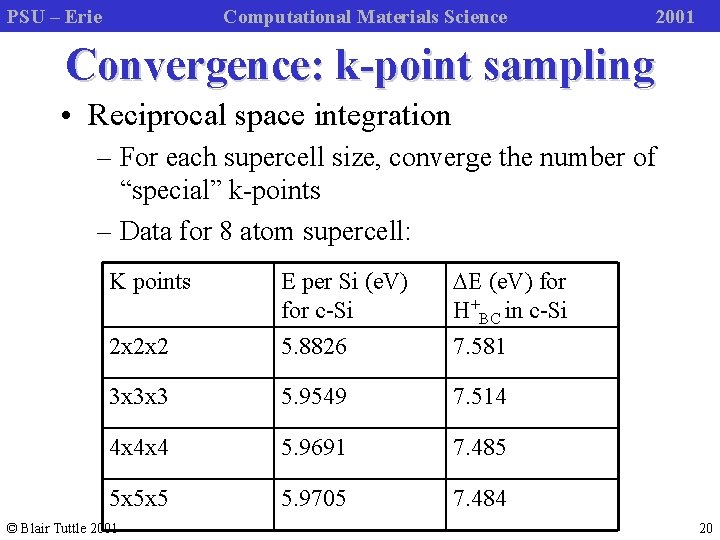
PSU – Erie Computational Materials Science 2001 Convergence: k-point sampling • Reciprocal space integration – For each supercell size, converge the number of “special” k-points – Data for 8 atom supercell: K points E per Si (e. V) for c-Si DE (e. V) for H+BC in c-Si 2 x 2 x 2 5. 8826 7. 581 3 x 3 x 3 5. 9549 7. 514 4 x 4 x 4 5. 9691 7. 485 5 x 5 x 5 5. 9705 7. 484 © Blair Tuttle 2001 20

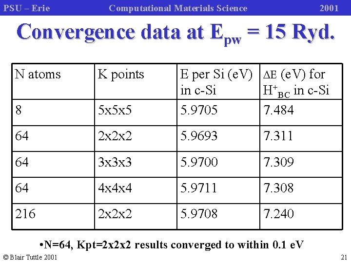
PSU – Erie Computational Materials Science 2001 Convergence data at Epw = 15 Ryd. N atoms K points 8 5 x 5 x 5 E per Si (e. V) DE (e. V) for in c-Si H+BC in c-Si 5. 9705 7. 484 64 2 x 2 x 2 5. 9693 7. 311 64 3 x 3 x 3 5. 9700 7. 309 64 4 x 4 x 4 5. 9711 7. 308 216 2 x 2 x 2 5. 9708 7. 240 • N=64, Kpt=2 x 2 x 2 results converged to within 0. 1 e. V © Blair Tuttle 2001 21

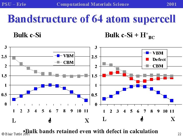
PSU – Erie Computational Materials Science 2001 Bandstructure of 64 atom supercell Bulk c-Si + H+BC G L X L G • Bulk bands retained even with defect in calculation © Blair Tuttle 2001 X 22

PSU – Erie Computational Materials Science 2001 Results for H in c-Si EForm Eglda H+1 H 0 H-1 0. 5 e. V 1. 0 e. V EFermi • H 0 and H+1 at global minimum • H-1 at stationary point or saddle point – Will lower its energy by moving to Td site For more info see: C. G. Van de Walle, “Hydrogen in crystalline semiconductors” Deep Centers I Semiconductors , Ed. by S. T. Pantelides, pg. 899 (1992). © Blair Tuttle 2001 23

PSU – Erie Computational Materials Science 2001 Hydrogen in Silicon Solid = LDA, Dashed =LDA + rigid scissor shift E in e. V Exp. LDA © Blair Tuttle 2001 E(0, -) 0. 51 0. 46 E(+, 0) 0. 92 1. 07 E(+, -) 0. 72 0. 77 U-corr -0. 41 -0. 61 24

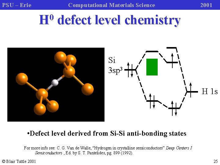
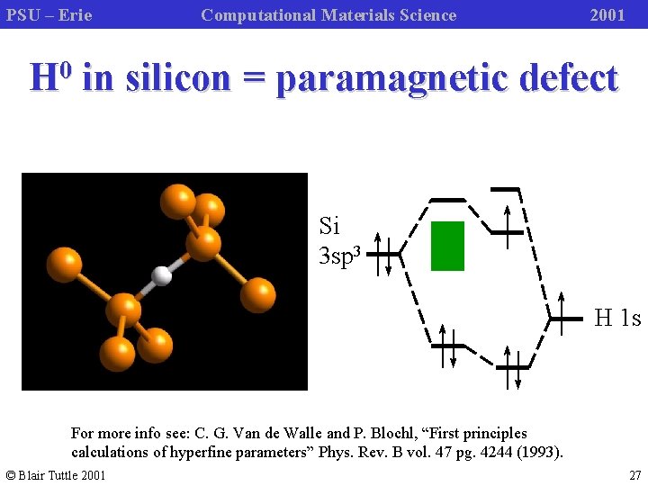
PSU – Erie Computational Materials Science 2001 H 0 defect level chemistry Si 3 sp 3 001 110 H 1 s • Defect level derived from Si-Si anti-bonding states For more info see: C. G. Van de Walle, “Hydrogen in crystalline semiconductors” Deep Centers I Semiconductors , Ed. by S. T. Pantelides, pg. 899 (1992). © Blair Tuttle 2001 25

PSU – Erie Computational Materials Science 2001 Metal Oxide Semiconductor Field Effect Transistor (MOSFET) Source © Blair Tuttle 2001 Gate Drain Lds ~ 90 nm tox ~ 2. 0 nm Vsd ~ 2. 0 V 26

PSU – Erie 0 H Computational Materials Science 2001 in silicon = paramagnetic defect Si 3 sp 3 001 110 H 1 s For more info see: C. G. Van de Walle and P. Blochl, “First principles calculations of hyperfine parameters” Phys. Rev. B vol. 47 pg. 4244 (1993). © Blair Tuttle 2001 27

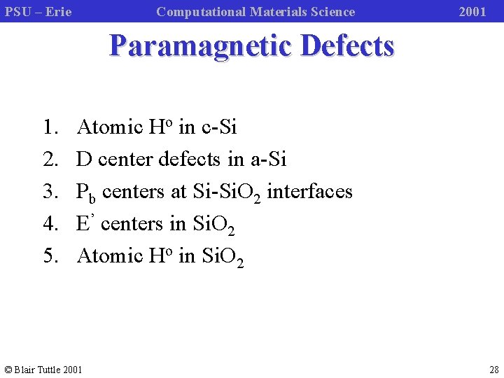
PSU – Erie Computational Materials Science 2001 Paramagnetic Defects 1. 2. 3. 4. 5. Atomic Ho in c-Si D center defects in a-Si Pb centers at Si-Si. O 2 interfaces E’ centers in Si. O 2 Atomic Ho in Si. O 2 © Blair Tuttle 2001 28

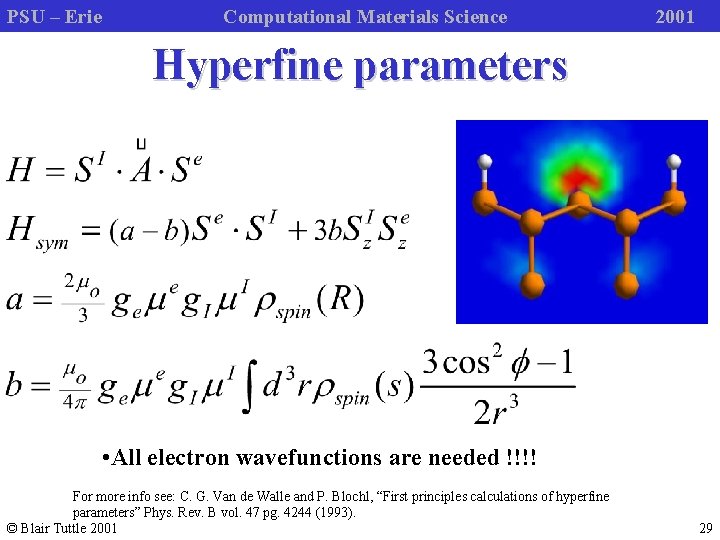
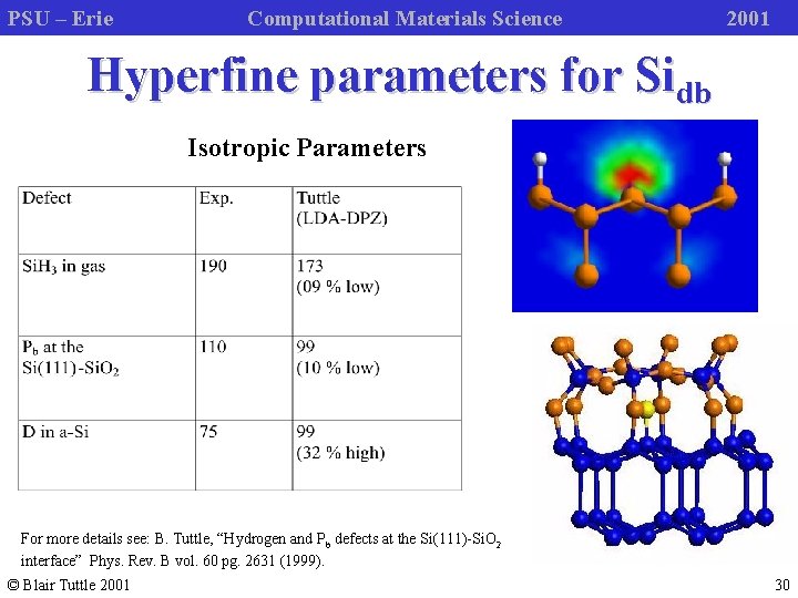
PSU – Erie Computational Materials Science 2001 Hyperfine parameters • All electron wavefunctions are needed !!!! For more info see: C. G. Van de Walle and P. Blochl, “First principles calculations of hyperfine parameters” Phys. Rev. B vol. 47 pg. 4244 (1993). © Blair Tuttle 2001 29

PSU – Erie Computational Materials Science 2001 Hyperfine parameters for Sidb Isotropic Parameters For more details see: B. Tuttle, “Hydrogen and Pb defects at the Si(111)-Si. O 2 interface” Phys. Rev. B vol. 60 pg. 2631 (1999). © Blair Tuttle 2001 30

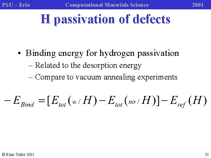
PSU – Erie Computational Materials Science 2001 H passivation of defects • Binding energy for hydrogen passivation – Related to the desorption energy – Compare to vacuum annealing experiments © Blair Tuttle 2001 31

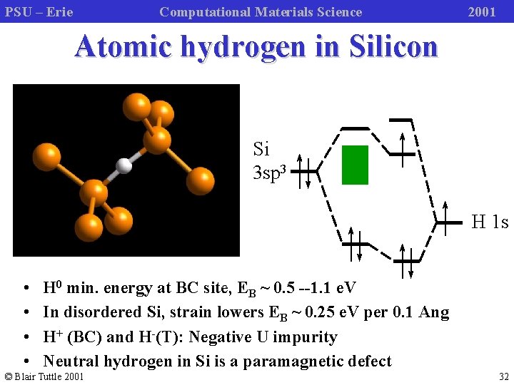
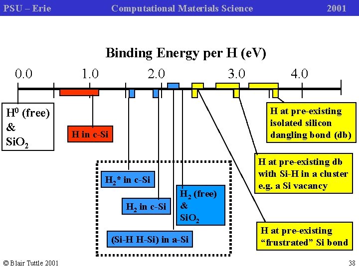
PSU – Erie Computational Materials Science 2001 Atomic hydrogen in Silicon 001 Si 3 sp 3 H 1 s • • 110 E ~ 0. 5 --1. 1 e. V H 0 min. energy at BC site, B In disordered Si, strain lowers EB ~ 0. 25 e. V per 0. 1 Ang H+ (BC) and H-(T): Negative U impurity Neutral hydrogen in Si is a paramagnetic defect © Blair Tuttle 2001 32

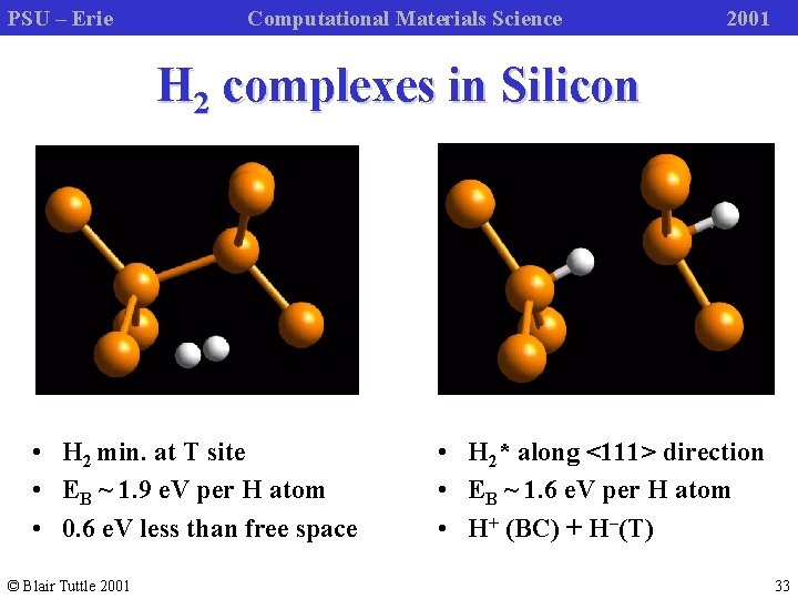
PSU – Erie Computational Materials Science 2001 H 2 complexes in Silicon • H 2 min. at T site • EB ~ 1. 9 e. V per H atom • 0. 6 e. V less than free space © Blair Tuttle 2001 • H 2* along <111> direction • EB ~ 1. 6 e. V per H atom _ • H+ (BC) + H (T) 33

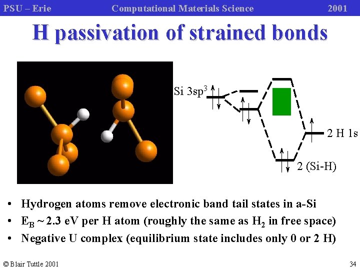
PSU – Erie Computational Materials Science 2001 H passivation of strained bonds Si 3 sp 3 2 H 1 s 2 (Si-H) • Hydrogen atoms remove electronic band tail states in a-Si • EB ~ 2. 3 e. V per H atom (roughly the same as H 2 in free space) • Negative U complex (equilibrium state includes only 0 or 2 H) © Blair Tuttle 2001 34

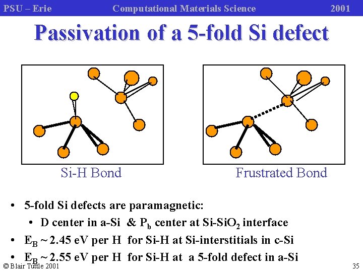
PSU – Erie Computational Materials Science 2001 Passivation of a 5 -fold Si defect Si-H Bond Frustrated Bond • 5 -fold Si defects are paramagnetic: • D center in a-Si & Pb center at Si-Si. O 2 interface • EB ~ 2. 45 e. V per H for Si-H at Si-interstitials in c-Si • EB ~ 2. 55 e. V per H for Si-H at a 5 -fold defect in a-Si © Blair Tuttle 2001 35

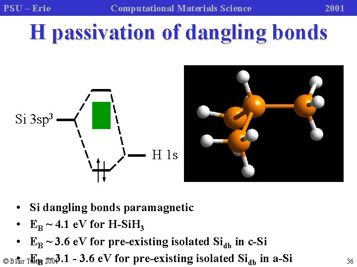
PSU – Erie Computational Materials Science 2001 H passivation of dangling bonds Si 3 sp 3 H 1 s • Si dangling bonds paramagnetic • EB ~ 4. 1 e. V for H-Si. H 3 • EB ~ 3. 6 e. V for pre-existing isolated Sidb in c-Si • Tuttle EB 2001 ~ 3. 1 - 3. 6 e. V for pre-existing isolated Sidb in a-Si © Blair 36

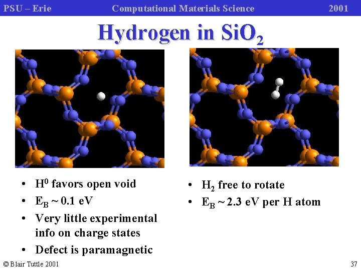
PSU – Erie Computational Materials Science 2001 Hydrogen in Si. O 2 • H 0 favors open void • EB ~ 0. 1 e. V • Very little experimental info on charge states • Defect is paramagnetic © Blair Tuttle 2001 • H 2 free to rotate • EB ~ 2. 3 e. V per H atom 37

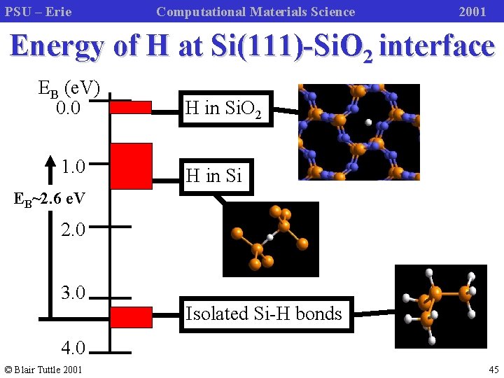
PSU – Erie Computational Materials Science 2001 Binding Energy per H (e. V) 0. 0 H 0 (free) & Si. O 2 1. 0 2. 0 3. 0 H at pre-existing isolated silicon dangling bond (db) H in c-Si H 2* in c-Si H 2 (free) & Si. O 2 (Si-H H-Si) in a-Si © Blair Tuttle 2001 4. 0 H at pre-existing db with Si-H in a cluster e. g. a Si vacancy H at pre-existing “frustrated” Si bond 38

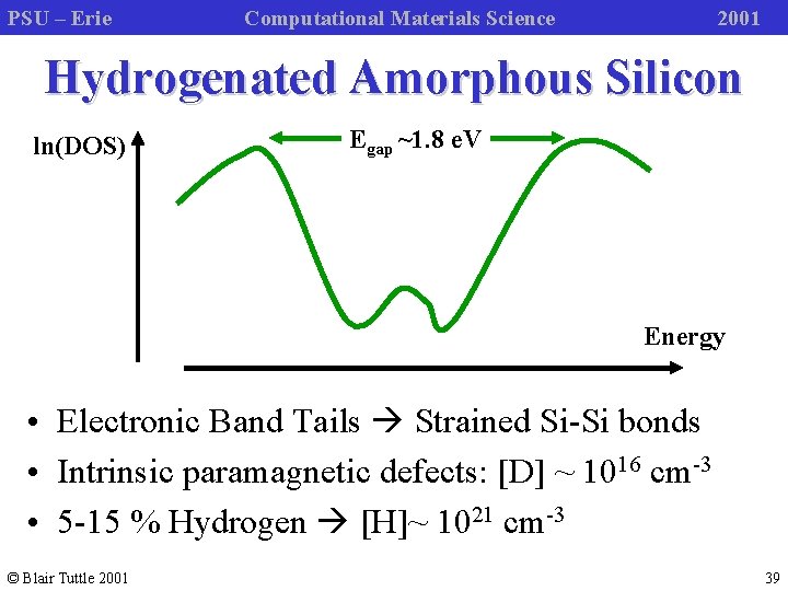
PSU – Erie Computational Materials Science 2001 Hydrogenated Amorphous Silicon ln(DOS) Egap ~1. 8 e. V Energy • Electronic Band Tails Strained Si-Si bonds • Intrinsic paramagnetic defects: [D] ~ 1016 cm-3 • 5 -15 % Hydrogen [H]~ 1021 cm-3 © Blair Tuttle 2001 39
![PSU Erie Computational Materials Science 2001 D concentration thermally activated with Ed PSU – Erie Computational Materials Science 2001 • [D] concentration thermally activated with Ed](https://slidetodoc.com/presentation_image/ab9be3cc92710ef741ce31ee55fb5d8a/image-40.jpg)
PSU – Erie Computational Materials Science 2001 • [D] concentration thermally activated with Ed ~ 0. 3 e. V • Hydrogen diffusion thermally activated Ea ~ 1. 5 e. V 1019 1018 1017 1019 1020 1021 H Evolved [cm-3] • Hydrogen in (Si-H H-Si) clusters evolves first • Dilute Si-H bonds stronger Spin Density [cm-3] Si-H behavior in a-Si: H 1018 1017 1016 S. Zafar and A. Schiff, “Hydrogen and defects in amorphous © Blair Tuttle 2001 silicon” Phys. Rev. Lett. Vol. 66 pg. 1493 (1991). 1. 2 1. 6 2. 0 1000/T [ k-1] 40

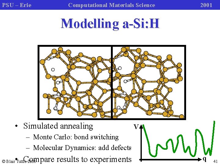
PSU – Erie Computational Materials Science 2001 Modelling a-Si: H • Simulated annealing V – Monte Carlo: bond switching – Molecular Dynamics: add defects • Compare results to experiments © Blair Tuttle 2001 q 41

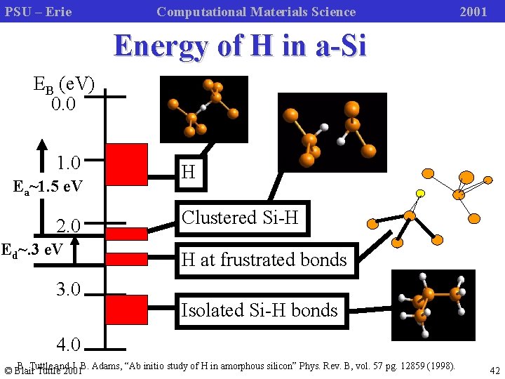
PSU – Erie Computational Materials Science 2001 Energy of H in a-Si EB (e. V) 0. 0 1. 0 Ea~1. 5 e. V 2. 0 Ed~. 3 e. V 3. 0 H Clustered Si-H H at frustrated bonds Isolated Si-H bonds 4. 0 B. Tuttle and J. B. Adams, “Ab initio study of H in amorphous silicon” Phys. Rev. B, vol. 57 pg. 12859 (1998). © Blair Tuttle 2001 42

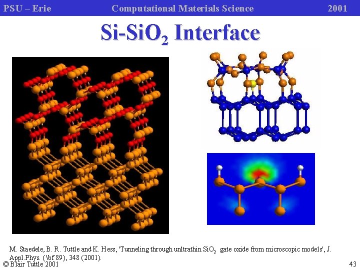
PSU – Erie Computational Materials Science 2001 Si-Si. O 2 Interface M. Staedele, B. R. Tuttle and K. Hess, 'Tunneling through unltrathin Si. O 2 gate oxide from microscopic models', J. Appl. Phys. {bf 89}, 348 (2001). © Blair Tuttle 2001 43

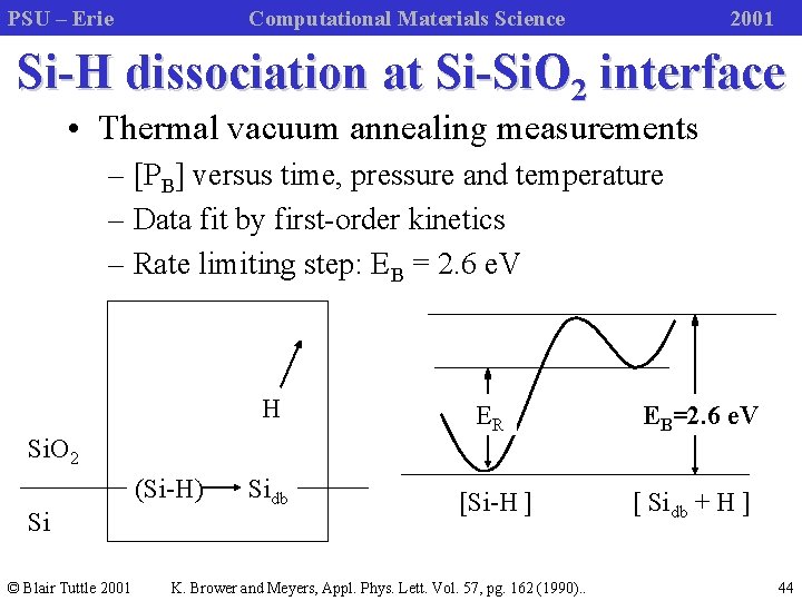
PSU – Erie Computational Materials Science 2001 Si-H dissociation at Si-Si. O 2 interface • Thermal vacuum annealing measurements – [PB] versus time, pressure and temperature – Data fit by first-order kinetics – Rate limiting step: EB = 2. 6 e. V H ER Sidb [Si-H ] Si. O 2 (Si-H) Si © Blair Tuttle 2001 K. Brower and Meyers, Appl. Phys. Lett. Vol. 57, pg. 162 (1990). . EB=2. 6 e. V [ Sidb + H ] 44

PSU – Erie Computational Materials Science 2001 Energy of H at Si(111)-Si. O 2 interface EB (e. V) 0. 0 1. 0 H in Si. O 2 H in Si EB~2. 6 e. V 2. 0 3. 0 Isolated Si-H bonds 4. 0 © Blair Tuttle 2001 45

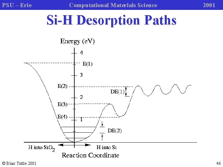
PSU – Erie Computational Materials Science 2001 Si-H Desorption Paths © Blair Tuttle 2001 46

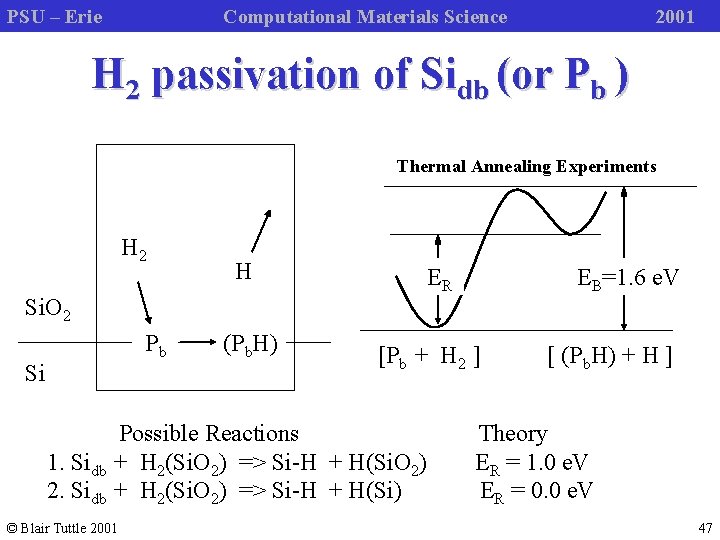
PSU – Erie Computational Materials Science 2001 H 2 passivation of Sidb (or Pb ) Thermal Annealing Experiments H 2 H ER Si. O 2 Pb Si (Pb. H) [Pb + H 2 ] Possible Reactions 1. Sidb + H 2(Si. O 2) => Si-H + H(Si. O 2) 2. Sidb + H 2(Si. O 2) => Si-H + H(Si) © Blair Tuttle 2001 EB=1. 6 e. V [ (Pb. H) + H ] Theory ER = 1. 0 e. V ER = 0. 0 e. V 47

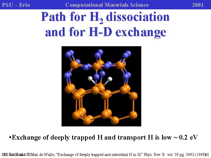
PSU – Erie Computational Materials Science 2001 Path for H 2 dissociation and for H-D exchange • Exchange of deeply trapped H and transport H is low ~ 0. 2 e. V ©B. Blair Tuttle 48 Tuttle and 2001 C. Van de Walle, “Exchange of deeply trapped and interstitial H in Si” Phys. Rev. B vol. 59 pg. 5493 (1999).

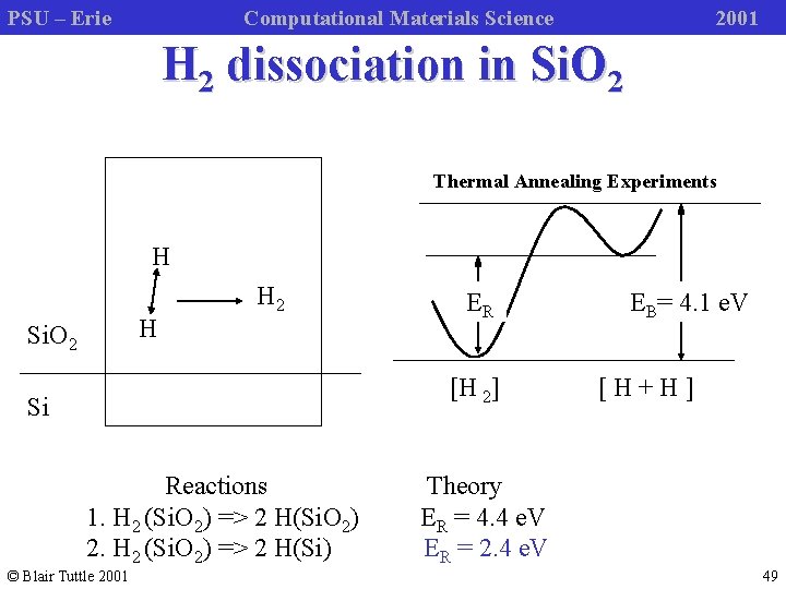
PSU – Erie Computational Materials Science 2001 H 2 dissociation in Si. O 2 Thermal Annealing Experiments H H Si. O 2 H 2 ER [H 2] Si Reactions 1. H 2 (Si. O 2) => 2 H(Si. O 2) 2. H 2 (Si. O 2) => 2 H(Si) © Blair Tuttle 2001 EB= 4. 1 e. V [H+H] Theory ER = 4. 4 e. V ER = 2. 4 e. V 49

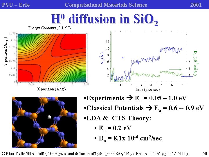
PSU – Erie Computational Materials Science 2001 H 0 diffusion in Si. O 2 Y position (Ang. ) Energy Contours (0. 1 e. V) X position (Ang. ) • Experiments Ea = 0. 05 – 1. 0 e. V • Classical Potentials Ea = 0. 6 -- 0. 9 e. V • LDA & CTS Theory: • Ea = 0. 2 e. V • Do = 8. 1 x 10 -4 cm 2/sec © Blair Tuttle 2001 B. Tuttle, “Energetics and diffusion of hydrogen in Si. O 2” Phys. Rev. B vol. 61 pg. 4417 (2000). 50

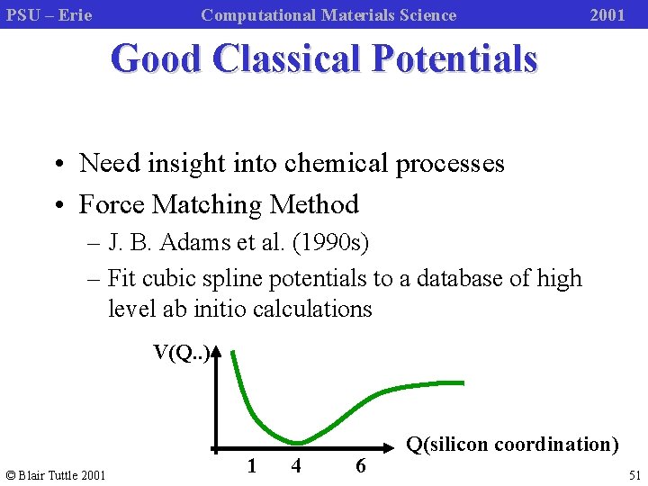
PSU – Erie Computational Materials Science 2001 Good Classical Potentials • Need insight into chemical processes • Force Matching Method – J. B. Adams et al. (1990 s) – Fit cubic spline potentials to a database of high level ab initio calculations V(Q. . ) © Blair Tuttle 2001 1 4 6 Q(silicon coordination) 51

PSU – Erie Computational Materials Science 2001 Summary • Computational methods based on DFT have been widely applied to important problems in materials science including point defects in semiconductors. • DFT methods provide a powerful tool for calculating properties of interest including: – Static properties (potential energy surfaces, formation energies, donor/acceptor levels) – Dynamical properties (vibrational frequencies, diffusivities) – Electrical and structural properties (defect levels, defect localization, hyperfine parameters) © Blair Tuttle 2001 52