PROCESSORS CONTROLLERS Course code 15 EM 2202 LTP


")
 TCON. 7 TCON. 6 TCON. 5 TCON. 4 TCON.")


")


 MOV")


 1 2 3 4 5 6 Vss Vcc VEE")


 INTERFACING ADCs( Analog-to-Digital Converters) are among the most widely used devices for data")


 This is")


 INTERFACING")


- Slides: 83
PROCESSORS & CONTROLLERS • Course code : 15 EM 2202 • L–T–P : 2– 2– 2 • Pre Requisite : 15 EC 1101 • Credits : 4
PROCESSORS AND CONTROLLERS 8086 Microprocessor: Introduction to Microprocessor, Intel Microprocessor families , 8086 Microprocessor architecture, Register Organization, Pin Description, Physical Memory Organization, Modes of operation. 8086 Instruction set & Assembly Language programming: Addressing modes, Instruction set, Assembler directives, simple Programs, Procedures and Macros, 8086 Interrupts.
PROCESSORS AND CONTROLLERS 8051 Microcontroller: Microcontroller families, 8051 Architecture, Signal Description, Register organization, Internal RAM, Special Function Registers, Interrupt control flow, Timer/Counter Operation, Serial Data Communication, and RS-232 C Standard. 8051 Programming & Interfacing: Addressing modes, Instruction set, Simple Programs involving Arithmetic and Logical Instructions, Timers/Counters, Serial Communication & Interrupts.
PROCESSORS AND CONTROLLERS PIC Microcontroller: Introduction, Architectural overview, Memory organization, interrupts and reset, I/O ports, Timers. Interfacing: Matrix Key Board, Stepper Motor, LCD’s, DAC & ADC. using 8051 and PIC Microcontroller.
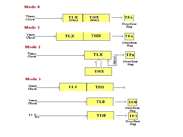
TIMERS The 8051 has two timers: 1. TIMER 0 2. TIMER 1 TIMER 0 TIMER 1
TMOD Register • • Gate : When set, timer only runs while INT(0, 1) is high. C/T : Counter/Timer select bit. M 1 : Mode bit 1. M 0 : Mode bit 0.
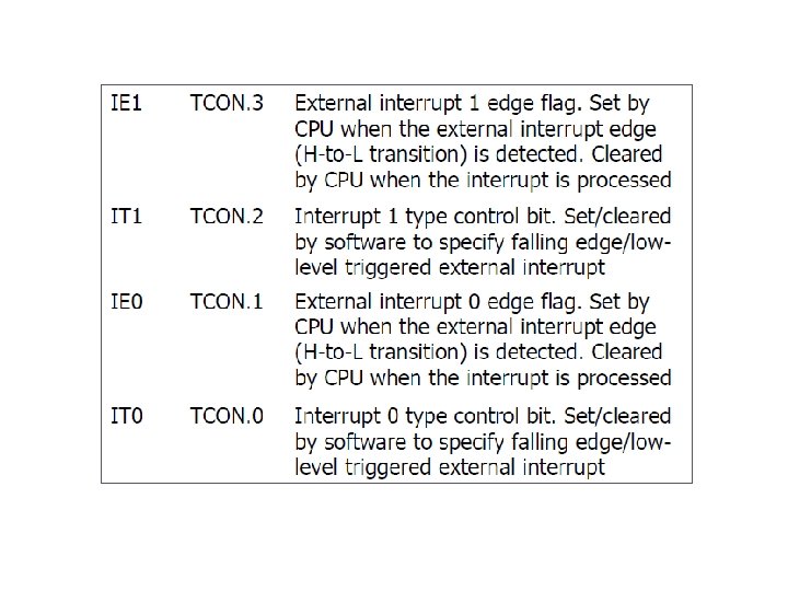
TCON Register (BIT ADRESSABLE REG) TCON. 7 TCON. 6 TCON. 5 TCON. 4 TCON. 3 TCON. 2 TCON. 1 TCON. 0 - TF 1: Timer 1 overflow flag. TR 1: Timer 1 run control bit. TF 0: Timer 0 overflag. TR 0: Timer 0 run control bit. IE 1: External interrupt 1 edge flag. IT 1: External interrupt 1 type flag. IE 0: External interrupt 0 edge flag. IT 0: External interrupt 0 type flag.
Concept of timer
GATE Control in TMOD If GATE = 1, the start and stop of the timer are done externally through pins P 3. 2 and P 3. 3 for timers 0 and 1, respectively
COUNTER Programming
Mode 1 Programming 1. Load the TMOD value register indicating which timer (Timer 0 or Timer 1) is to be used and which timer mode is selected. 2. Load registers TL & TH with initial count values. 3. Start the timer 4. Keep monitoring the timer flag(TF) 5. Stop the timer. 6. Clear TF for next round. 7. Go back to step 2 to load TH & TL again NOTE: MODE 0 is exactly like mode-1 except that it is 13 -bit timer instead 16 -bit. The 13 -bit timer/counter can hold values between 0000 H to 1 FFFH in TH-TL.
Mode 2 Programming 1. Load the TMOD value register indicating which timer (Timer 0 or Timer 1)is to be used, and select the timer mode (mode-2). 2. Load the TH register with the initial count value. 3. Start the timer. 4. Keep monitoring TF timer flag 5. After it becomes “ 1” then clear the TF flag 6. Go back to step 4 , since mode 2 is auto - reload
Example program for Mode 1 ORG 0 H MOV TMOD, #00000001 B BACK: MOV TL 0, #0 F 0 H MOV TH 0, #0 FFH CPL P 1. 0 ACALL DELAY SJMP BACK DELAY: SETB TR 0 HERE: JNB TF 0, HERE CLR TR 0 CLR TF 0 RET END
Example program for Mode 2 ORG 0 H MOV TMOD, #00100000 B MOV TH 1, #05 H SETB TR 1 HERE: JNB TF 1, HERE CPL P 2. 0 CLR TF 1 SJMP HERE END
Serial Communication
Serial vs. parallel Communication
Synchronous vs. Asynchronous Serial data communication uses two methods 1. Synchronous 2. Asynchronous There are special IC chips made by manufacturers for serial communications. 1. UART- universal asynchronous receiver-transmitter. 2. USART- universal synchronous - asynchronous receiver-transmitter
Framing (Asynchronous )
SCON register
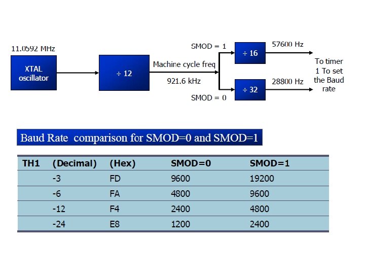
Doubling the baud rate There are two ways to increase the baud rate of data transfer in 8051. 1. Use a higher frequency crystal. 2. Change a D 7 -bit to 1 in the PCON register PCON Register: ( Byte addressable)
Programming 8051 to transfer data serially In programming 8051 to transfer character bytes serially, the following steps must be taken 1. The TMOD register is loaded with the value 20 H , indicating the use of Timer 1 in mode 2(8 -bit auto reload) to set the baud rate 2. The TH 1 is loaded with one of the values to set the baud rate for serial data transfer( assuming XTAL= 11. 0592 MHz). 3. The SCON register is loaded with the value 50 H indicating serial mode 1, where an 8 -bit data is framed with start & stop bits. 4. TR 1 is SET to 1 to start Timer 1. 5. TI is cleared when transmission is complete. 6. The character byte to be transferred serially is written into SBUF register. 7. TI is monitored for transmission. 8. To transfer the next character go to step 5
Example Program for Serial Communication ORG 0 H MOV TMOD, #00100000 B------(20 H) MOV TH 1, #-3 MOV SCON, #01010000 B-------(50 H) SETB TR 1 AGAIN: MOV A, # ” “ ACALL TRANSFER MOV A, # ”K“ ACALL TRANSFER MOV A, # ”L“ ACALL TRANSFER MOV A, # ”U“ TRANSFER: ACALL TRANSFER HERE: MOV A, # ” “ ACALL TRANSFER SJMP AGAIN END MOV SBUF, A JNB TI, HERE CLR TI RET
Interrupts
Concept behind Interrupt An interrupt is an external or internal event that interrupts the microcontroller to inform it that a device needs its service Upon activation of an interrupt, the microcontroller goes through the following steps 1. It finishes the instruction it is executing and saves the address of the next instruction (PC) on the stack 2. It also saves the current status of all the interrupts internally (i. e. : not on the stack) 3. It jumps to a fixed location in memory, called the interrupt vector table, that holds the address of the ISR 4. The microcontroller gets the address of the ISR from the interrupt vector table and jumps to it 5. Upon executing the RETI instruction, the microcontroller returns to the place where it was interrupted
Interrupts & Interrupt vectors:
Interrupt Enable Register
TCON REGISTER
LEVEL TRIGGERED INTERRUPT In level triggered interrupt to ensure the activation of the hardware interrupt at the INT ‘n’ pin, make sure that the duration of the low-level signal is around 4 machine cycles.
In edge-triggered interrupts • The external source must be held high for at least one machine cycle, and then held low for at least one machine cycle • The falling edge of pins INT 0 and INT 1 are latched by the 8051 and are held by the TCON. 1 and TCON. 3 bits of TCON register
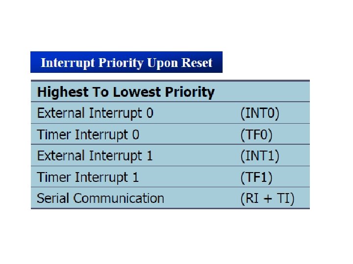
Interrupt Priority register
EXAMPLE PROGRAMS Write a program that continuously get 8 -bit data from P 0 and sends it to P 1 while simultaneously creating a square wave of 200 μs period on pin P 2. 1. Use timer 0 to create the square wave. Assume that XTAL = 11. 0592 MHz. END ORG 0000 H LJMP MAIN ORG 000 BH CPL P 2. 1 RETI ORG 0030 H MAIN: MOV TMOD, #02 H MOV P 0, #0 FFH MOV TH 0, #-92 (TH 0=A 4 H) MOV IE, #82 H SETB TR 0 BACK: MOV A, P 0 MOV P 1, A SJMP BACK
EXAMPLE PROGRAMS Write a program to generate a square wave if 50 Hz frequency on pin P 1. 2. Assume that XTAL=11. 0592 MHz ORG 0 LJMP MAIN ORG 000 BH CPL P 1. 2 MOV TL 0, #00 MOV TH 0, #0 DCH RETI ORG 30 H MAIN: MOV TM 0 D, #00000001 B MOV TL 0, #00 MOV TH 0, #0 DCH MOV IE, #82 H SETB TR 0 HERE: SJMP HERE END
EXAMPLE PROGRAMS Write a program in which the 8051 reads data from P 1 and writes it to P 2 continuously while giving a copy of it to the serial COM port to be transferred serially. Assume that XTAL=11. 0592. Set the baud rate at 9600 ORG 0000 H LJMP MAIN ORG 23 H LJMP SERIAL ORG 30 H MAIN: MOV P 1, #0 FFH MOV TMOD, #20 H MOV TH 1, #0 FDH MOV SCON, #50 H MOV IE, #10010000 B SETB TR 1 BACK: MOV A, P 1 MOV SBUF, A MOV P 2, A SJMP BACK ORG 100 H SERIAL: JB TI, TRANS MOV A, SBUF CLR RI RETI TRANS: CLR TI RETI END
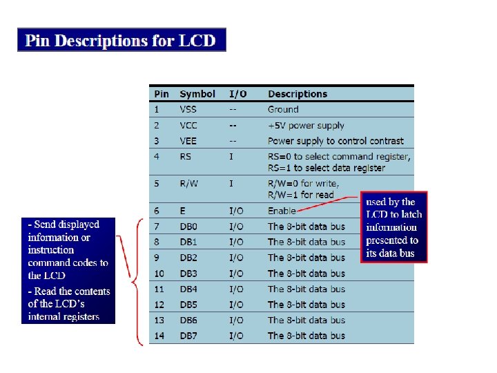
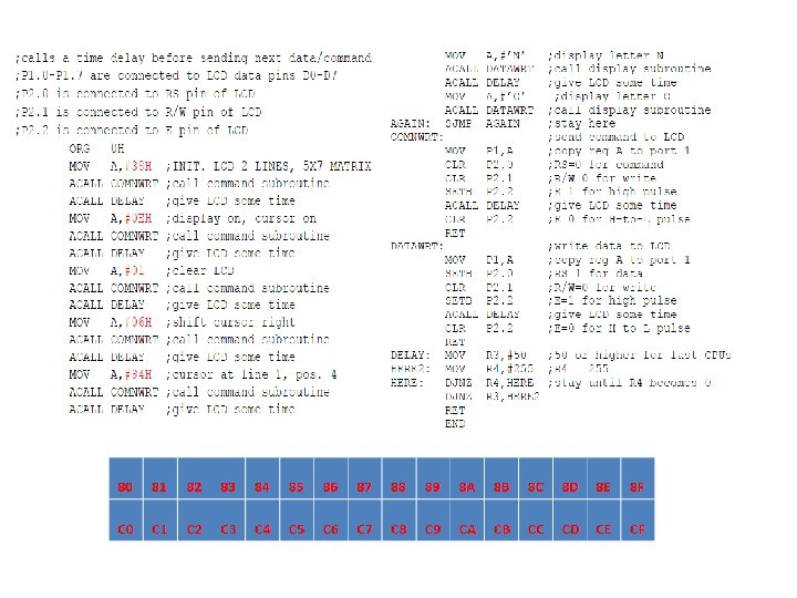
LCD Interfacing (16 X 2) 1 2 3 4 5 6 Vss Vcc VEE RS R/W EN LCD 7 8 9 10 11 12 13 14 DB 0 ----------------------- DB 7 15 16 + -
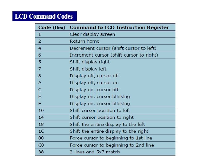
Addresses of 16 x 2 LCD 80 81 82 83 84 85 86 87 88 89 8 A 8 B 8 C 8 D 8 E 8 F C 0 C 1 C 2 C 3 C 4 C 5 C 6 C 7 C 8 C 9 CA CB CC CD CE CF
LCD INTERFACING TO 8051
STEPPER MOTOR INTERFACING Ø A Stepper motor is a widely used device that translates electrical pulses into mechanical movement. Ø In applications such as disk drives, dot matrix printers & robotics, the stepper motor is used for position control Ø Stepper motors commonly have a permanent magnet ‘rotor’( also called shaft) surrounded by a ‘stator’.
Stator Windings Configuration
Driving Stepper motor Normal 4 Step Sequence CLOCKWISE STEP WINDING A WINDING B WINDING C WINDING D 1 1 1 0 0 2 0 1 1 0 3 0 0 1 1 4 1 0 0 1 COUNTER CLOCKWISE Wave Drive 4 step sequence CLOCKWISE STEP WINDING A WINDING B WINDING C WINDING D 1 1 0 0 0 2 0 1 0 0 3 0 0 1 0 4 0 0 0 1 COUNTER CLOCKWISE
Driving Stepper motor Half step 8 -step sequence Step Sequence CLOCKWISE STEP WINDING A WINDING B WINDING C WINDING D 1 1 0 0 0 2 1 1 0 0 3 0 1 0 0 4 0 1 1 0 5 0 0 1 0 6 0 0 1 1 7 0 0 0 1 8 1 0 0 1 COUNTER CLOCKWISE
Interfacing Circuit
ULN 2803
Stepper Motor Program Assuming two stepper motors are interfaced to 8051 with ULN 2803 drivers. Program for normal 4 -step sequence ( clock wise ) ORG 0 H BACK: END MOV A, #0 CCH MOV P 1, A ACALL DELAY MOV A, #66 H MOV P 1, A ACALL DELAY MOV A, #33 H MOV P 1, A ACALL DELAY MOV A, #99 H MOV P 1, A ACALL DELAY SJMP BACK DELAY: LOOP 2: LOOP 1: MOV R 0, #0 FFH MOV R 1, #80 H DJNZ R 1, LOOP 1 DJNZ R 0, LOOP 2 RET
Stepper Motor Program Assuming two stepper motors are interfaced to 8051 with ULN 2803 drivers. Program for wave drive 4 -step sequence ( clock wise ) ORG 0 H BACK: END MOV A, #88 H MOV P 1, A ACALL DELAY MOV A, #44 H MOV P 1, A ACALL DELAY MOV A, #22 H MOV P 1, A ACALL DELAY MOV A, #11 H MOV P 1, A ACALL DELAY SJMP BACK DELAY: LOOP 2: LOOP 1: MOV R 0, #0 FFH MOV R 1, #80 H DJNZ R 1, LOOP 1 DJNZ R 0, LOOP 2 RET
Stepper Motor Program Assuming two stepper motors are interfaced to 8051 with ULN 2803 drivers. Program for half step 8 -step sequence ( clock wise ) ORG 0 H BACK: MOV A, #88 H MOV P 1, A ACALL DELAY MOV A, #0 CCH MOV P 1, A ACALL DELAY MOV A, #44 H MOV P 1, A ACALL DELAY MOV A, #66 H MOV P 1, A ACALL DELAY MOV A, #22 H MOV P 1, A ACALL DELAY MOV A, #33 H MOV P 1, A ACALL DELAY MOV A, #11 H MOV P 1, A ACALL DELAY MOV A, #99 H MOV P 1, A ACALL DELAY SJMP BACK END DELAY: LOOP 2: LOOP 1: RET MOV R 0, #0 FFH MOV R 1, #80 H DJNZ R 1, LOOP 1 DJNZ R 0, LOOP 2
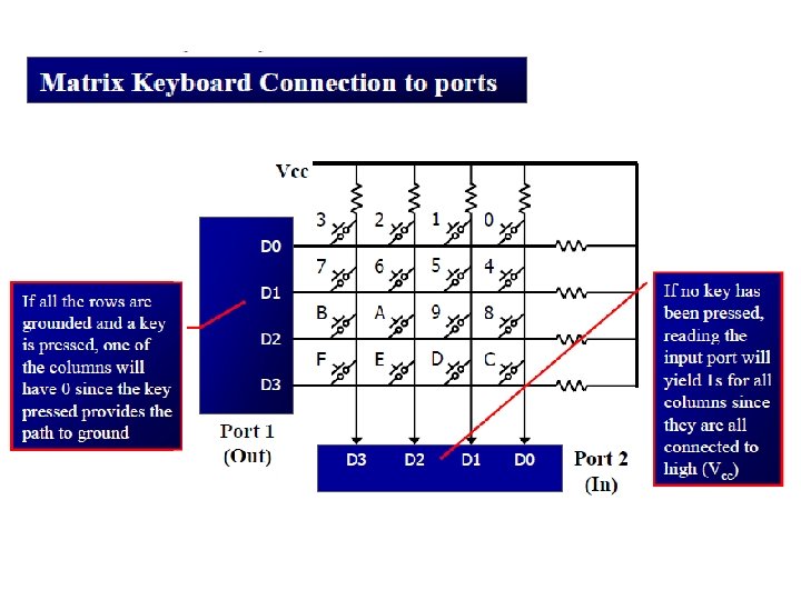
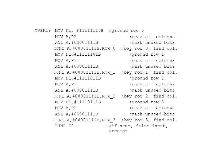
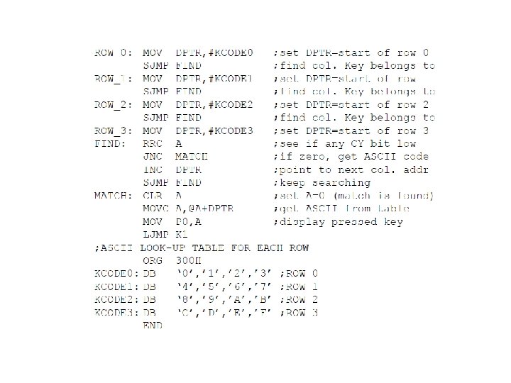
KEYBOARD INTERFACING
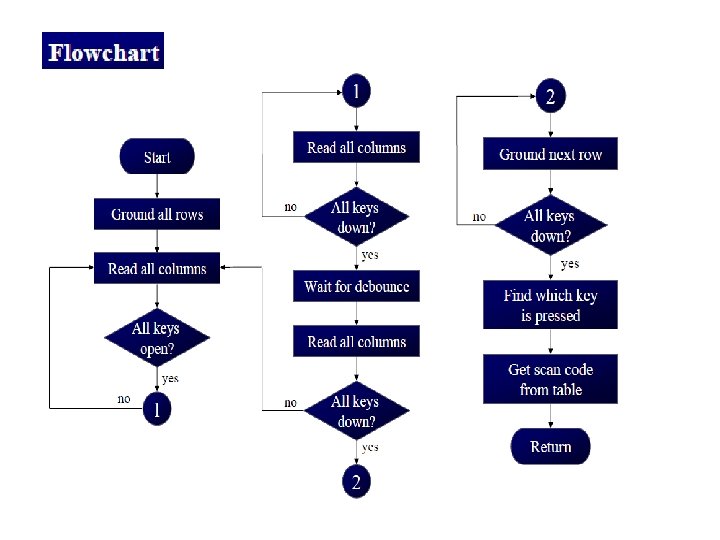
Keyboard Program
ADC(0804) INTERFACING ADCs( Analog-to-Digital Converters) are among the most widely used devices for data acquisition. A Physical quantity, like temperature, pressure, humidity, and velocity, etc. , is converted to electrical ( Voltage , current) signals using a device called a transducer or sensor. We need ADCs to translate the analog signals to digital numbers, so that the microprocessor/microcontroller can read the data for further implement.
ADC 0804
Important Points on ADC 0804 1. Vcc It works with +5 volts and has a resolution of 8 bits. 2. Conversion time is another major factor in judging an ADC. a. Conversion time is defined as the time it takes the ADC to convert the analog input to a digital (Binary) number. b. In ADC 804 conversion time varies depending on the clocking signals applied to CLK R and CLK IN pins, but it cannot be faster than 110 μs
3. CLK IN and CLK R a. CLK IN is an input pin connected to an external clock source b. To use the internal clock generator (also called self clocking), CLK IN and CLK R pins are connected to a capacitor and a resistor, and the clock frequency is determined by Typical values are R = 10 K ohms and C = 150 p. F. We get f = 606 k. Hz and the conversion time is 110 μs.
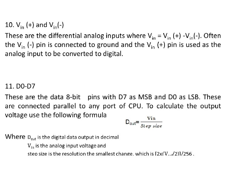
4. VRef/2: It is used for the reference voltage § If this pin is open (not connected), the analog input voltage is in the range of 0 to 5 volts (the same as the Vcc pin) § If the analog input range needs to be 0 to 4 volts, VRef/2 is connected to 2 volts
5. Analog ground and digital ground § Analog ground is connected to the ground of the analog Vin. § Digital ground is connected to the ground of the Vcc pin. 6. CS( Chip Select) Chip select is an active low input used to activate the ADC 0804 chip. 7. RD(Read) This is an input signal and is active low. The ADC converts the analog input to its binary equivalent and holds it in an internal register. RD is used to get the converted data out of the ADC 0804 chip. When CS=0, if a high-to-low pulse is applied to the RD pin, the 8 -bit digital output can be read from D 0 -D 7. The RD pin is also referred to as Output Enable(OE).
8. WR( Write , a better name might be “start of Conversion”) This is an active low input used to inform the ADC 0804 to start the conversion process. If CS=0, when WR makes a low-to-high transition, the ADC 0804 starts converting the analog input value of Vin to an 8 -bit digital number 9. INTR( Interrupt, a better name might be “End of Conversion”) This is an output pin and is active low. It is normally high pin and when the conversion is completed, it goes low to signal the CPU that the converted data is ready to be picked up. After INTR goes low, we make CS=0 and send a high- to- low pulse to the RD pin to get the next analog data to be converted.
Timing diagram of ADC 0804
Interfacing circuit of ADC 0804
Program for ADC 0804 HERE: RD BIT P 2. 5 WR BIT P 2. 6 INTR BIT P 2. 7 MYDATA EQU P 1 MOV P 1, #0 FFH SETB INTR CLR WR SETB WR JB INTR, HERE CLR RD MOV A, MYDATA ACALL CONVERSION ACALL DATA_DISPLAY SETB RD SJMP BACK
DAC(0808) INTERFACING
Interfacing Circuit of DAC 0808
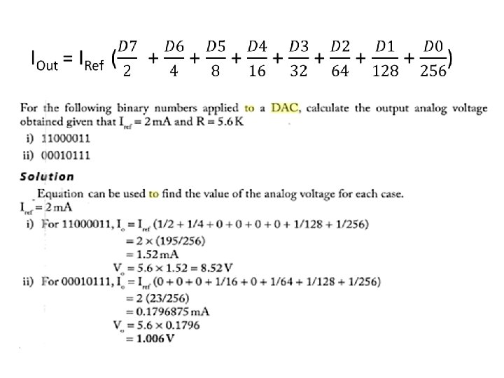
Specifications related to DAC 1. Resolution: It can be defined as a smallest change in the output corresponding to an input change by one LSB. 2. Accuracy: This is the measure of the difference between the actual output voltage & the expected output voltage. 3. Full scale output voltage: This is the output voltage when binary input has the highest value. For ex: 8 -bit 5 V DAC have max voltage 5 V-19. 5 mv= 4. 9805 V.
Generating Staircase waveform ORG 0 H START: CLR A AGAIN: MOV P 1, A INC A ACALL DELAY CJNE A, #0 FFH, GO SJMP START GO: SJMP AGAIN DELAY: LOOP: END MOV R 0, #0 FFH DJNZ R 0, LOOP RET ; Send data to DAC ; count from 0 h to FFh ; Let DAC recover
Generating Triangular waveform ORG 0 H START 0 to 1: AGAIN 1: GO 1: START 1 to 0: GO 2: END CLR A MOV P 1, A INC A ACALL DELAY CJNE A, #0 FFH, GO 1 SJMP START 1 to 0 SJMP AGAIN 1 MOV P 1, A DEC A ACALL DELAY CJNE A, #00 H, GO 2 SJMP START 0 to 1 SJMP START 1 to 0 ; Send data to DAC ; count from 0 h to FFh ; Let DAC recover DELAY: LOOP: MOV R 0, #0 FFH DJNZ R 0, LOOP RET
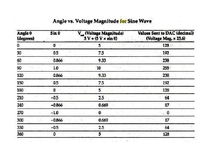
Generating Sine waveform To generate a sine wave , we first need a table whose values represent the magnitude of the sine of angles between 00 & 3600 The values for the sine function vary from -1. 0 to +1. 0 for 00 & 3600 angles. Therefore, the table values are integer numbers representing the voltage magnitude for the sine of theta (θ). To generate sine wave we assume the full scale voltage of 10 V for DAC output. Full scale output of the DAC is achieved when all the data inputs of the DAC are high. Therefore, to achieve the full scale 10 V output, we use the following equation. VOut = 5 V + ( 5 X Sin θ)
Example
Program ORG 0 H BACK: MOV DPTR, #TABLE MOV R 2, #COUNT CLR A MOVC A, @A+DPTR MOV P 1, A INC DPTR DJNZ R 2, BACK SJMP AGAIN ORG 0300 H TABLE: DB 128, 192, 238, 255, 238, 192, 128, 64, 17, 0, 17, 64, 128
Representation of Sine waveform Volts 10 9 8 7 6 5 4 3 2 1 0 30 60 90 120 150 180 210 240 270 300 330 Degrees 360