PLL Phase Locked Loop Concept PLL compares the
 Concept • PLL compares the phase of the input signal")


 Input Signal Phase detector Vc(t) VCO v(t)")
![Therefore, the general equation of the PLL is Vc(t) = KD [ i(t) v(t)]](https://slidetodoc.com/presentation_image_h2/acab4612cafeb7ced115b61c35f55f8f/image-14.jpg "Therefore, the general equation of the PLL is Vc(t) = KD [ i(t) v(t)]")


- Slides: 46
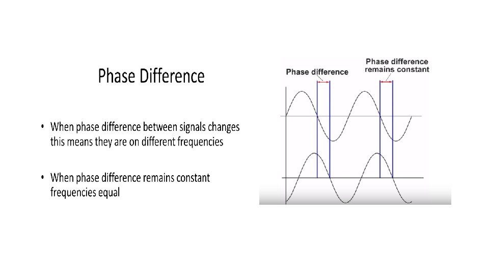
PLL (Phase Locked Loop) Concept • PLL compares the phase of the input signal with the phase of an internally generated periodic signal (typically sine or square wave) and uses a negative feedback to make the two phases equal. • Equal phase means equal frequencies ; which is the reason for PLL • If an input signal is suddenly applied to a PLL circuit, the circuit takes finite amount of time to respond at the end, the phases of the input and internally generated signals are equal, independent of time, then the PLL is said to be LOCKED. • It is also known as Phase difference– to- Voltage Converter.
PLL are mainly used in – – 2/12/2022 FM demodulators Signal Re constituion Clock Recovery Frequency synthesis , etc. ,
2/12/2022
PLL Building Blocks • • 2/12/2022 Phase Detector VCO Loop filter Error Amplifier
2/12/2022
2/12/2022
2/12/2022
PLL 2/12/2022
Applications 1. PLL are integral part of many communications systems and many digital systems. 2. Used in frequency demodulation and phase demodulation 3. Frequency synthesis – generating rational multiples of fixed input frequencies. 4. Clock Generation and Recovery 5. Reduction of Jitter in Circuits 6. Used in radar signal synchronization. 2/12/2022
Why PLL 2/12/2022
PLL Working 2/12/2022
Block Diagram of First order PLL i(t) Input Signal Phase detector Vc(t) VCO v(t) • The phase detector produces an output voltage vc(t), which is proportional to the difference in the phases of the input voltage and VCO output voltage Vv(t). [ Phase diff to voltage converter] • The output of the PD is fed to the VCO. • The frequency of the output signal of the VCO is directly proportional to its input voltage called control voltage Vc(t).
Therefore, the general equation of the PLL is Vc(t) = KD [ i(t) v(t)] v(t) = FR + K 0 Vc(t) Where i and v are the total phases of the input and VCO signals KD is the gain of the Phase detector in V/rad. v is the frequency of the VCO output FR is the free running frequency, the natural oscillation frequency of the VCO when control input voltage is zero. And K 0 is the voltage to frequency conversion factor of the VCO in rad/s V.
PLL – IC 565 It is a closed loop system designed to lock the frequency and phase of the output to the frequency and phase of an input signal. PLL are available as inexpensive monolithic ICs. IC 565 is a popular PLL IC. It is 14 pin IC. In this all components are integrated as a single chip. IC 565 Consists of • Phase Detector • Low Pass Filter • Error Amplifier and • VCO 2/12/2022
565 PLL Block Diagram 2/12/2022
Operation • The phase detector is a multiplier which multiplies the two input signals and gives the sum and difference component as o/p. • The low pass filter passes the difference component and attenuate the sum frequency component. • The error amplifier produces the dc voltage signal proportional to the difference in frequency. • This dc voltage is applied to the VCO (Voltage Controlled Oscillator) and it produces corresponding changes in the frequency. • This process repeat until the error is zero. Then the PLL is said to be locked.
• 2/12/2022
• 2/12/2022
2/12/2022
2/12/2022
2/12/2022
2/12/2022
Frequency Multiplier • In electronics, a frequency multiplier is an electronic circuit that generates an output signal whose output frequency is a harmonic (multiple) of its input frequency. • A divide by N network is inserted between VCO output (pin 4) and phase comparator input (pin 5). Since the output of the divider is locked to the input signal frequency ‘fi‘ the VCO is running at the multiple of input frequency. In the locked state the output frequency of the VCO is given by f 0 = N. fi • By using proper divide by N circuit, it is possible to obtain desired multiplication. 2/12/2022
2/12/2022
2/12/2022
2/12/2022
Circuit Description of frequency multiplier To verify the operation of the circuit frequency multiplier, one must determine the input frequency range and then adjust the free running frequency f. OUT of the VCO by mean of R 1 and C 1 so that the output frequency of the 7490 divider is midway within the predetermined input frequency range. The output of the VCO now should be 5 f. IN. The output frequency f. OUT can be adjusted from 1. 5 KHz to 15 KHz by varying potentiometer R 1 (f. OUT = 1. 2/4 R 1 C 1). This means that the input frequency f. IN range has to be within 300 Hz to 3 KHz. In addition, the input waveform can either be sine or square wave and may be applied to input pin 2 or 3. Even though supply voltages of ± 10 V are used in figure 1 1, the NE 565 can be operated on ± 5 supply voltage instead. A small capacitor C 3 typically 1000 p. F, is connected between pins 7 and 8 to eliminate possible oscillations. Also, capacitor C 2 should be large enough to stabilize the VCO frequency.
2/12/2022
2/12/2022
2/12/2022
• the two resulting frequencies corre spondto the logic 0 and logic 1 states of the binary data signal. • The frequencies corresponding to logic 1 and logic 0 states are commonly called the mark and space frequencies. Several standards are used to set the mark and space frequencies. 2/12/2022
Demodulator using 565 2/12/2022
An FSK signal demodulator can be built as illustrated in figure. • The demodulator receives a signal at one of the two distinct carrier frequencies, 1, 270 Hz or 1, 070 Hz representing the RS 232 C logic levels of mark ( 5 V) or space (+ 14 V), respectively. • Capacitance coupling is used at the input to remove a dc level. As the signal appears at the input of 565 PLL, the PLL locks to the input frequency and tracks it between the two possible frequencies with a corresponding dc shift at the output. • Resistor R 1 and capacitor C 1 determine the free running frequency of the VCO =(1170 Hz). • Capacitor C 2 is a loop filter capacitor that establishes the dynamic characteristics of the demodulator. • Capacitor C 2 is chosen smaller than usual one to eliminate overshoot on the output pulse. • A three stage RC ladder filter is employed for removing the sum frequency component from the output. 2/12/2022
The VCO frequency is adjusted with R 1 so that the dc voltage level at the output (pin 7) is the same as that at pin 6. An input at frequency 1, 070 Hz drives the demodulator output voltage to a more positive voltage level, driving the digital output to the high level (space or + 14 V). An input at 1, 270 Hz correspondingly drives the 565 dc output less positive with the digital output, which then drops to the low level (mark or – 5 V). 2/12/2022
2/12/2022
2/12/2022
2/12/2022
2/12/2022
2/12/2022
2/12/2022
2/12/2022
2/12/2022
2/12/2022
2/12/2022
2/12/2022