Low jitter PLL design Jeffrey Prinzie 16 05


- Slides: 45

Low jitter PLL design Jeffrey Prinzie 16 -05 -2017

Content • Basic PLL concepts • Phase noise and jitter • Noise sources in PLLs • Phase noise in VCOs 2

Content • Basic PLL concepts • Phase noise and jitter • Noise sources in PLLs • Phase noise in VCOs 3

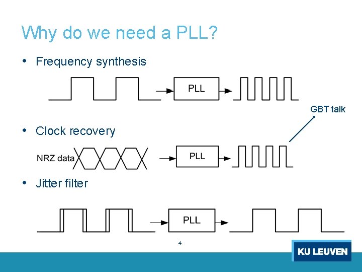
Why do we need a PLL? • Frequency synthesis GBT talk • Clock recovery • Jitter filter 4

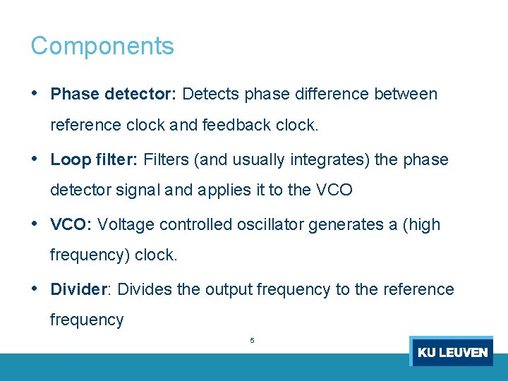
Components • Phase detector: Detects phase difference between reference clock and feedback clock. • Loop filter: Filters (and usually integrates) the phase detector signal and applies it to the VCO • VCO: Voltage controlled oscillator generates a (high frequency) clock. • Divider: Divides the output frequency to the reference frequency 5

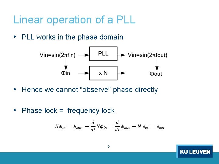
Linear operation of a PLL • PLL works in the phase domain • Hence we cannot “observe” phase directly • Phase lock = frequency lock 6

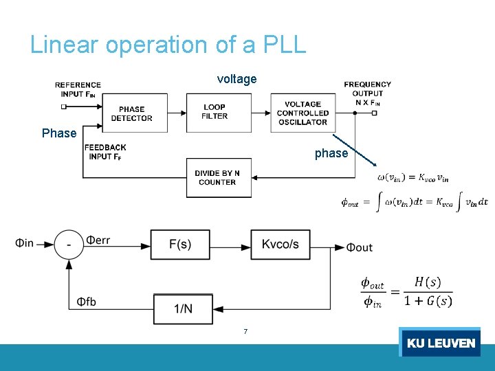
Linear operation of a PLL voltage Phase phase 7

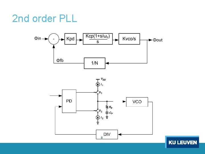
2 nd order PLL 8

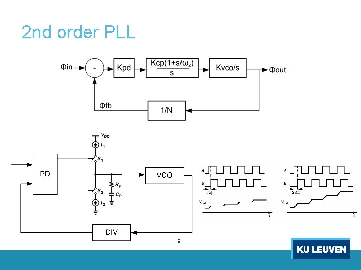
2 nd order PLL 9

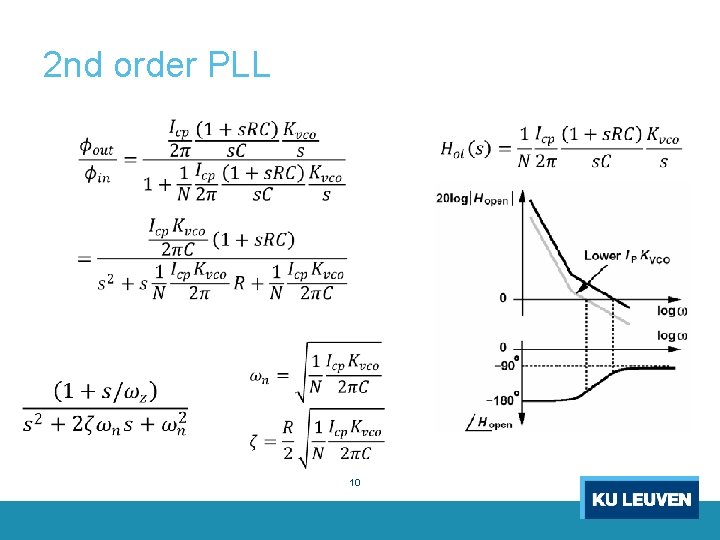
2 nd order PLL 10

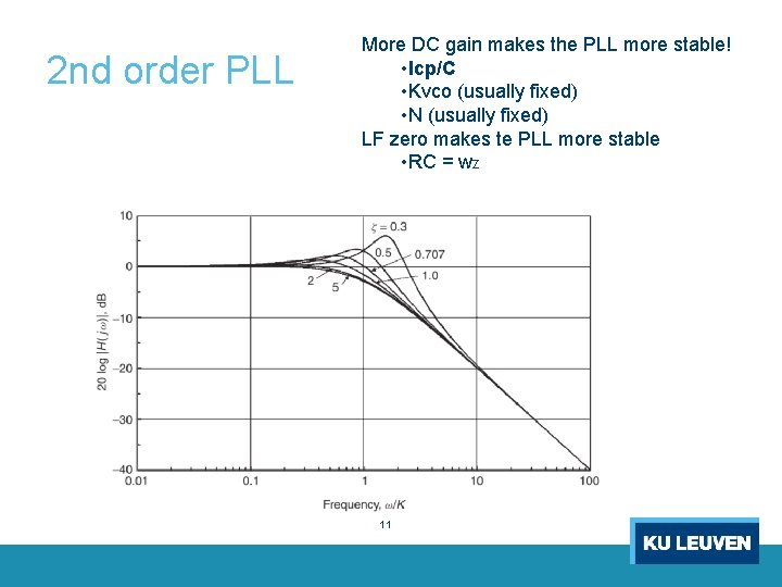
2 nd order PLL More DC gain makes the PLL more stable! • Icp/C • Kvco (usually fixed) • N (usually fixed) LF zero makes te PLL more stable • RC = wz 11

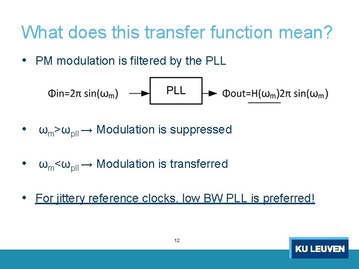
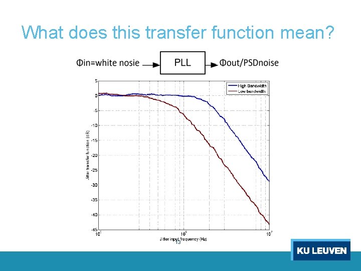
What does this transfer function mean? • PM modulation is filtered by the PLL • ωm>ωpll → Modulation is suppressed • ωm<ωpll → Modulation is transferred • For jittery reference clocks, low BW PLL is preferred! 12

What does this transfer function mean? 13

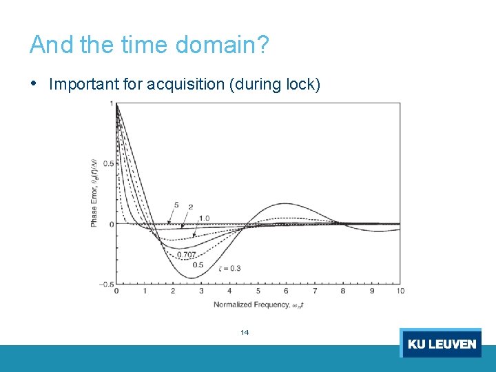
And the time domain? • Important for acquisition (during lock) 14

Content • Basic PLL concepts • Phase noise and jitter • Noise sources in PLLs • Phase noise in VCOs 15

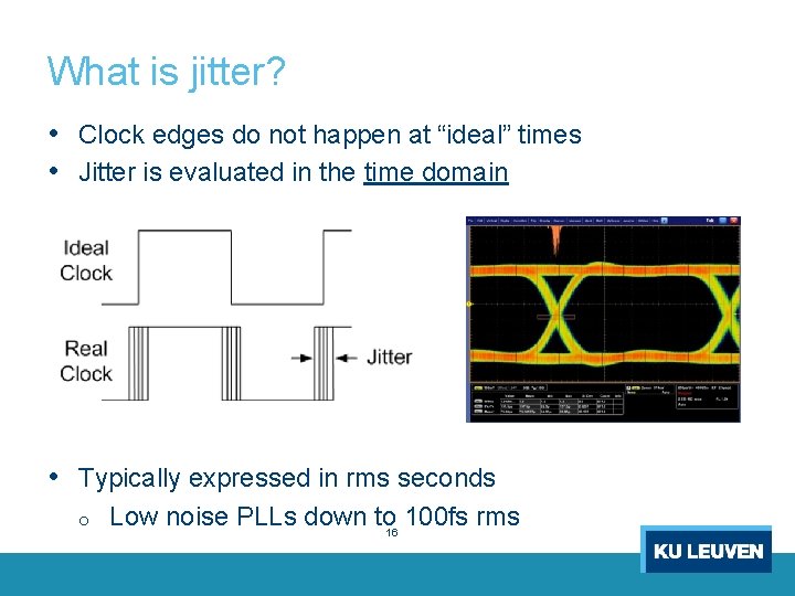
What is jitter? • Clock edges do not happen at “ideal” times • Jitter is evaluated in the time domain • Typically expressed in rms seconds o Low noise PLLs down to 16 100 fs rms

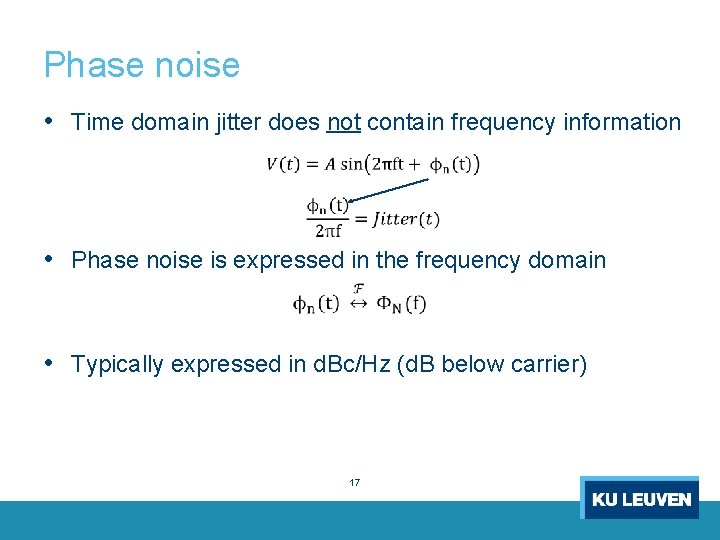
Phase noise • Time domain jitter does not contain frequency information • Phase noise is expressed in the frequency domain • Typically expressed in d. Bc/Hz (d. B below carrier) 17

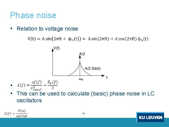
Phase noise • Relation to voltage noise • • This can be used to calculate (basic) phase noise in LC oscillators 18

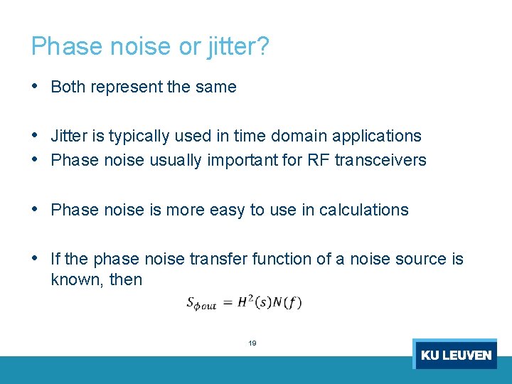
Phase noise or jitter? • Both represent the same • Jitter is typically used in time domain applications • Phase noise usually important for RF transceivers • Phase noise is more easy to use in calculations • If the phase noise transfer function of a noise source is known, then 19

Content • Basic PLL concepts • Phase noise and jitter • Noise sources in PLLs • Phase noise in VCOs 20

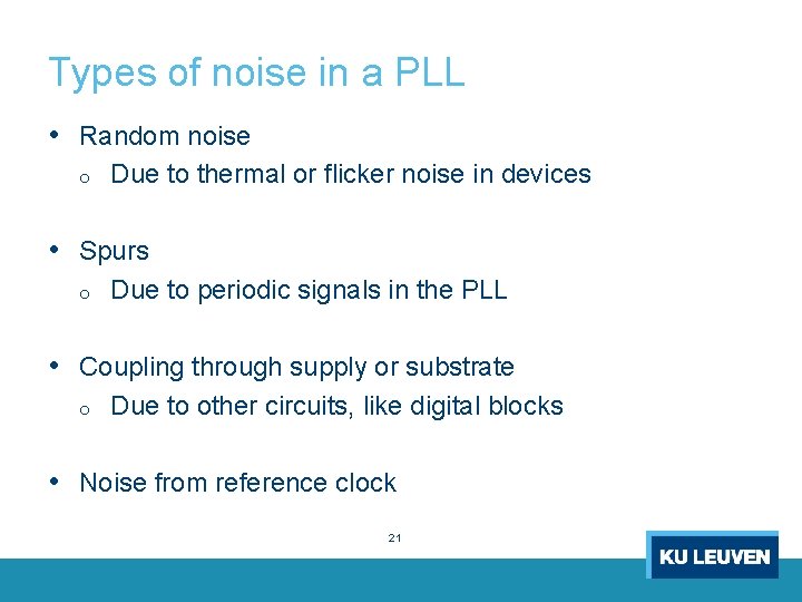
Types of noise in a PLL • Random noise o Due to thermal or flicker noise in devices • Spurs o Due to periodic signals in the PLL • Coupling through supply or substrate o Due to other circuits, like digital blocks • Noise from reference clock 21

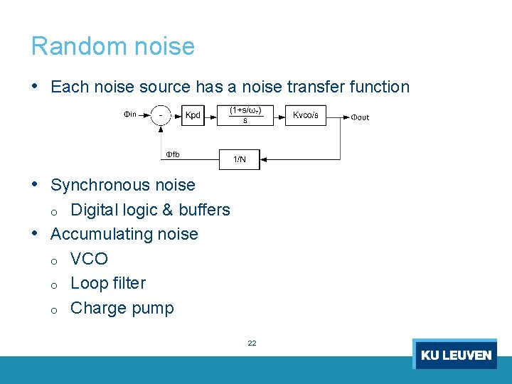
Random noise • Each noise source has a noise transfer function • Synchronous noise Digital logic & buffers • Accumulating noise o VCO o Loop filter o Charge pump o 22

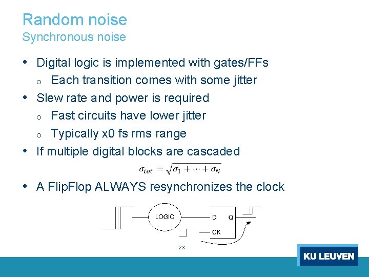
Random noise Synchronous noise • Digital logic is implemented with gates/FFs Each transition comes with some jitter • Slew rate and power is required o Fast circuits have lower jitter o Typically x 0 fs rms range • If multiple digital blocks are cascaded o • A Flip. Flop ALWAYS resynchronizes the clock 23

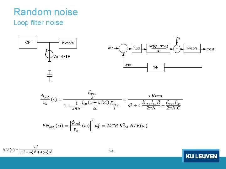
Random noise Loop filter noise 24

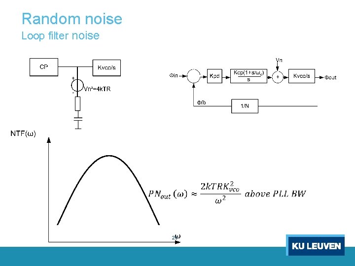
Random noise Loop filter noise 25

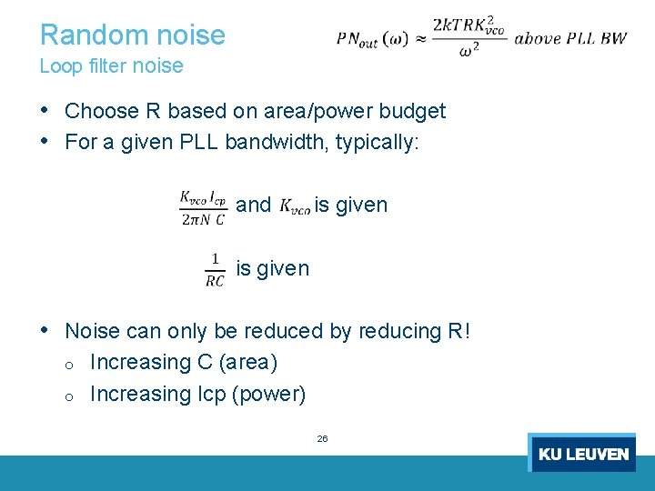
Random noise Loop filter noise • Choose R based on area/power budget • For a given PLL bandwidth, typically: and is given • Noise can only be reduced by reducing R! o o Increasing C (area) Increasing Icp (power) 26

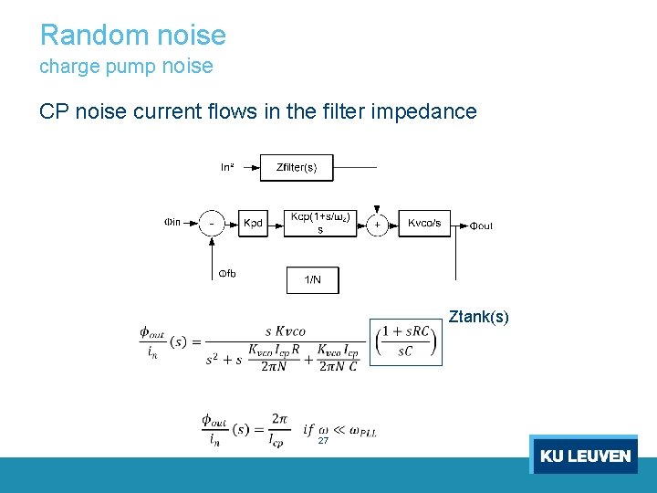
Random noise charge pump noise CP noise current flows in the filter impedance Ztank(s) 27

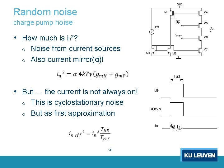
Random noise charge pump noise • How much is in²? o o Noise from current sources Also current mirror(α)! • But … the current is not always on! o o This is cyclostationary noise But as first approximation 28

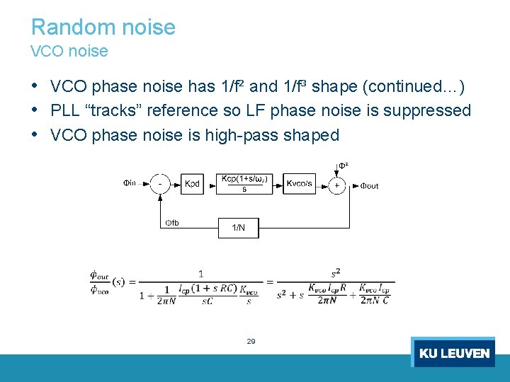
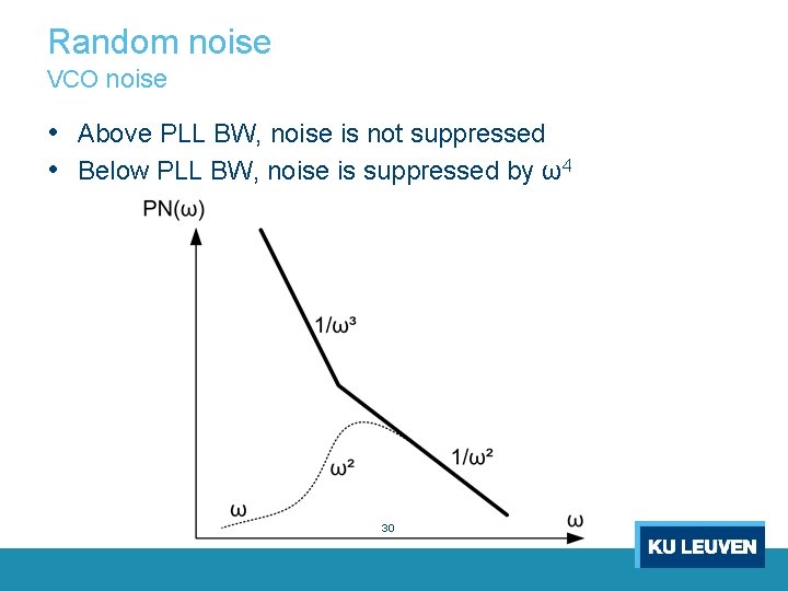
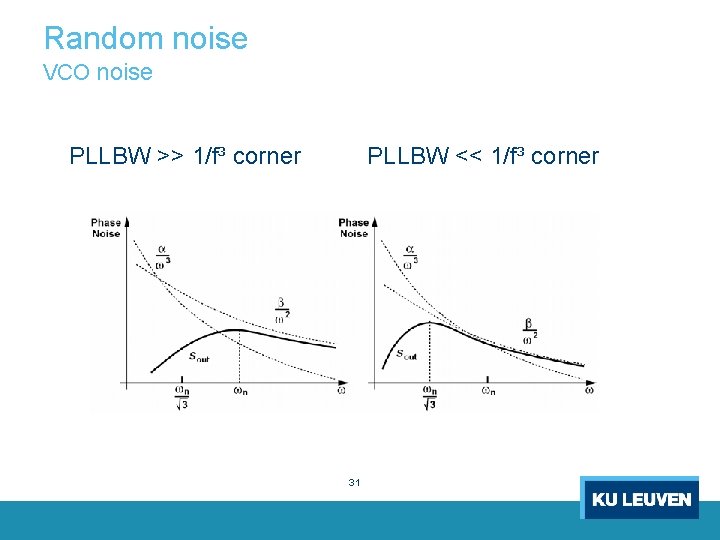
Random noise VCO noise • VCO phase noise has 1/f² and 1/f³ shape (continued…) • PLL “tracks” reference so LF phase noise is suppressed • VCO phase noise is high-pass shaped 29

Random noise VCO noise • Above PLL BW, noise is not suppressed • Below PLL BW, noise is suppressed by ω4 30

Random noise VCO noise PLLBW >> 1/f³ corner PLLBW << 1/f³ corner 31

Content • Basic PLL concepts • Phase noise and jitter • Noise sources in PLLs • Phase noise in VCOs 32

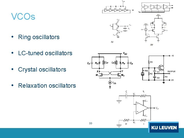
VCOs • Ring oscillators • LC-tuned oscillators • Crystal oscillators • Relaxation oscillators 33

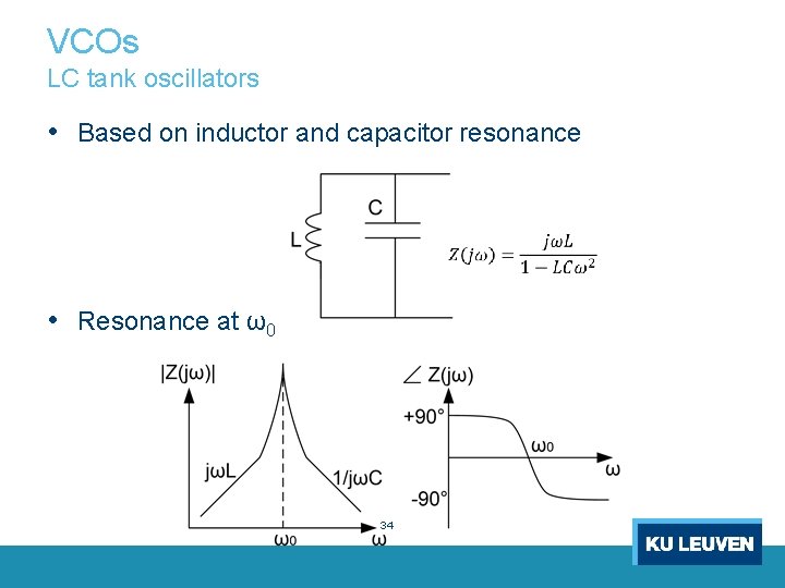
VCOs LC tank oscillators • Based on inductor and capacitor resonance • Resonance at ω0 34

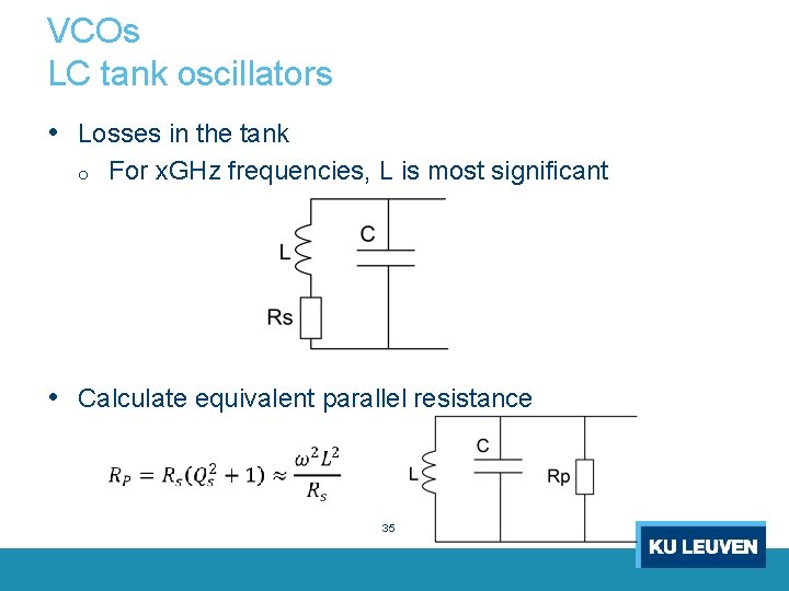
VCOs LC tank oscillators • Losses in the tank o For x. GHz frequencies, L is most significant • Calculate equivalent parallel resistance 35

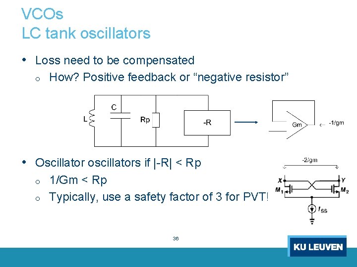
VCOs LC tank oscillators • Loss need to be compensated o How? Positive feedback or “negative resistor” • Oscillator oscillators if |-R| < Rp o o 1/Gm < Rp Typically, use a safety factor of 3 for PVT! 36

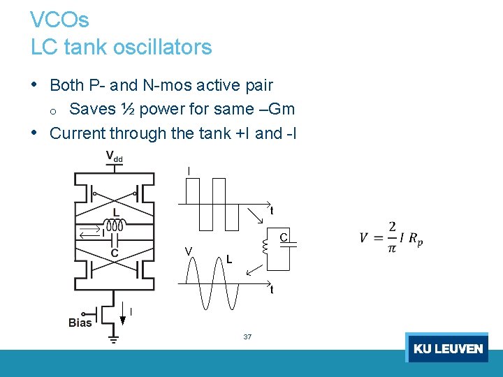
VCOs LC tank oscillators • Both P- and N-mos active pair Saves ½ power for same –Gm • Current through the tank +I and -I o 37

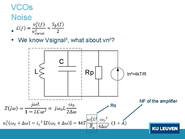
VCOs Noise • • We know Vsignal², what about vn²? Rs 38 NF of the amplifier

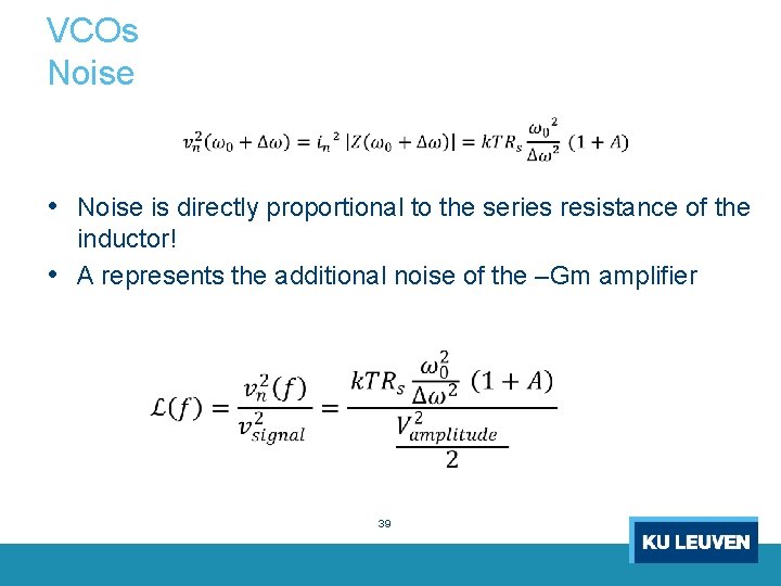
VCOs Noise • Noise is directly proportional to the series resistance of the inductor! • A represents the additional noise of the –Gm amplifier 39

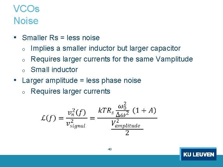
VCOs Noise • Smaller Rs = less noise Implies a smaller inductor but larger capacitor o Requires larger currents for the same Vamplitude o Small inductor • Larger amplitude = less phase noise o Requires larger currents o 40

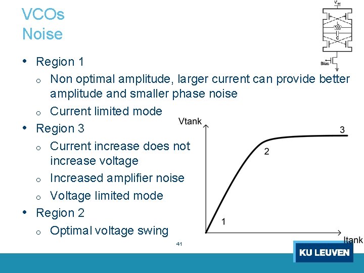
VCOs Noise • Region 1 Non optimal amplitude, larger current can provide better amplitude and smaller phase noise o Current limited mode • Region 3 o Current increase does not increase voltage o Increased amplifier noise o Voltage limited mode • Region 2 o Optimal voltage swing o 41

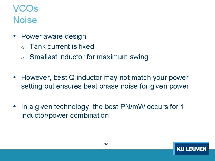
VCOs Noise • Power aware design o o Tank current is fixed Smallest inductor for maximum swing • However, best Q inductor may not match your power setting but ensures best phase noise for given power • In a given technology, the best PN/m. W occurs for 1 inductor/power combination 42

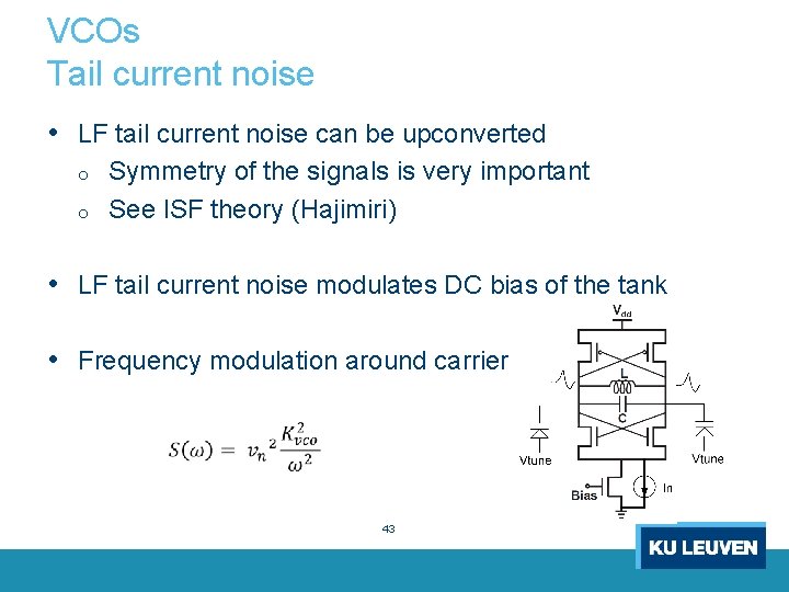
VCOs Tail current noise • LF tail current noise can be upconverted o o Symmetry of the signals is very important See ISF theory (Hajimiri) • LF tail current noise modulates DC bias of the tank • Frequency modulation around carrier 43

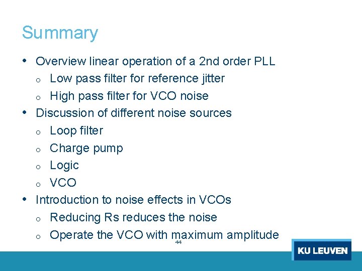
Summary • Overview linear operation of a 2 nd order PLL Low pass filter for reference jitter o High pass filter for VCO noise • Discussion of different noise sources o Loop filter o Charge pump o Logic o VCO • Introduction to noise effects in VCOs o Reducing Rs reduces the noise o Operate the VCO with maximum amplitude 44 o

Thank you Jeffrey. Prinzie@kuleuven. be