DLL Design for Low Power and Jitter Yanqing
- Slides: 35
DLL Design for Low Power and Jitter Yanqing Zhang yanqing@virginia. edu
Outline � DLL Quick Review � Seminal Papers � First “dual loop” with infinite phase capture range � First true dual loop architecture � Summary of DLL Design Issues � A Walk Through Time � The first all digital DLL (1999) � The first mixed mode DLL (1999) � Process variation problem � False lock problem � Fast lock acquisition � PFD jitter � CP jitter � Summary of DLL Design Space � Discussion Questions
Outline � DLL Quick Review � Seminal Papers � First “dual loop” with infinite phase capture range � First true dual loop architecture � Summary of DLL Design Issues � A Walk Through Time � The first all digital DLL (1999) � The first mixed mode DLL (1999) � Process variation problem � False lock problem � Fast lock acquisition � PFD jitter � CP jitter � Summary of DLL Design Space � Discussion Questions
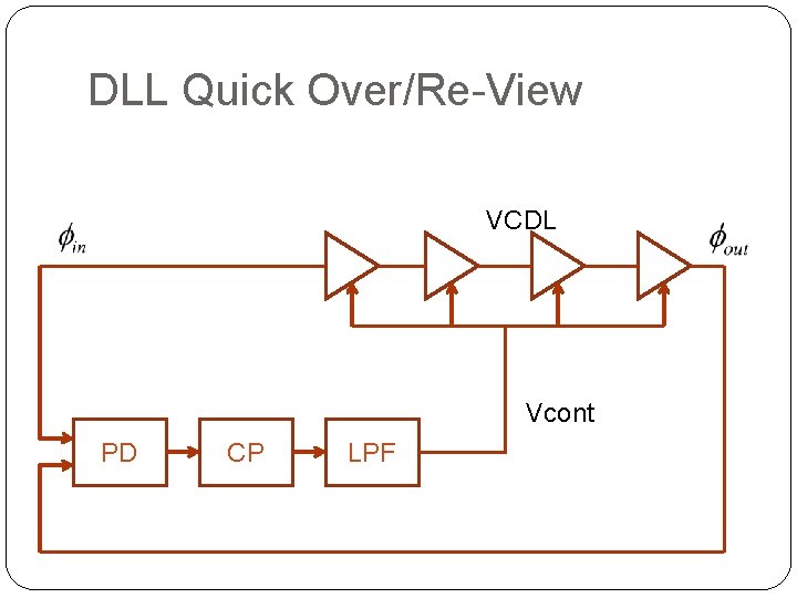
DLL Quick Over/Re-View VCDL Vcont PD CP LPF
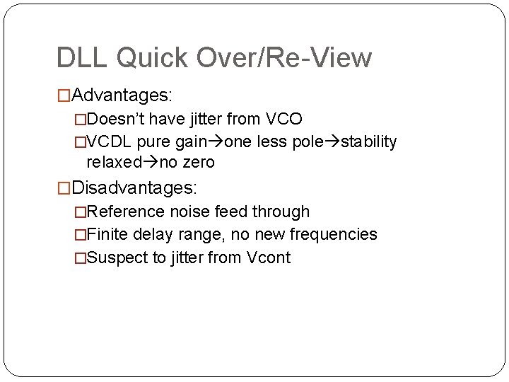
DLL Quick Over/Re-View �Advantages: �Doesn’t have jitter from VCO �VCDL pure gain one less pole stability relaxed no zero �Disadvantages: �Reference noise feed through �Finite delay range, no new frequencies �Suspect to jitter from Vcont
Outline � DLL Quick Review � Seminal Papers � First “dual loop” with infinite phase capture range � First true dual loop architecture � Summary of DLL Design Issues � A Walk Through Time � The first all digital DLL (1999) � The first mixed mode DLL (1999) � Process variation problem � False lock problem � Fast lock acquisition � PFD jitter � CP jitter � Summary of DLL Design Space � Discussion Questions
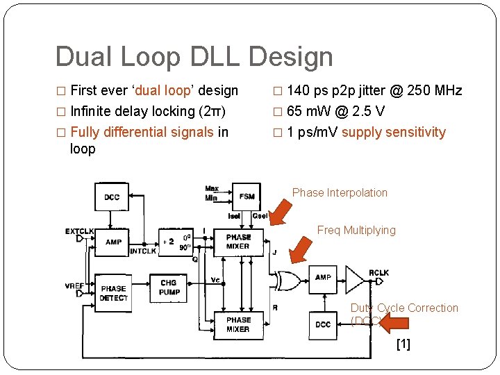
Dual Loop DLL Design � First ever ‘dual loop’ design � 140 ps p 2 p jitter @ 250 MHz � Infinite delay locking (2π) � 65 m. W @ 2. 5 V � Fully differential signals in � 1 ps/m. V supply sensitivity loop Phase Interpolation Freq Multiplying Duty Cycle Correction (DCC) [1]
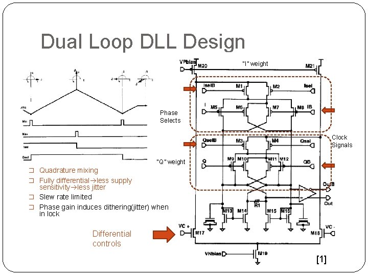
Dual Loop DLL Design “I” weight Phase Selects Clock Signals “Q” weight � Quadrature mixing � Fully differential less supply sensitivity less jitter � Slew rate limited � Phase gain induces dithering(jitter) when in lock Differential controls [1]
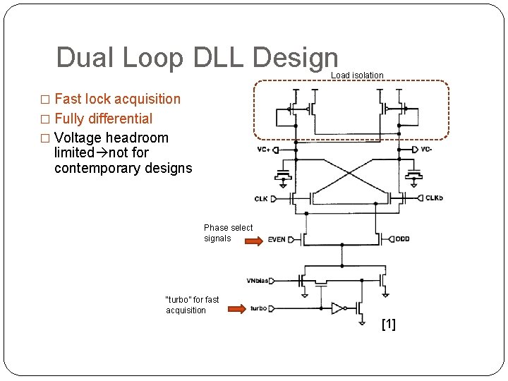
Dual Loop DLL Design Load isolation � Fast lock acquisition � Fully differential � Voltage headroom limited not for contemporary designs Phase select signals “turbo” for fast acquisition [1]
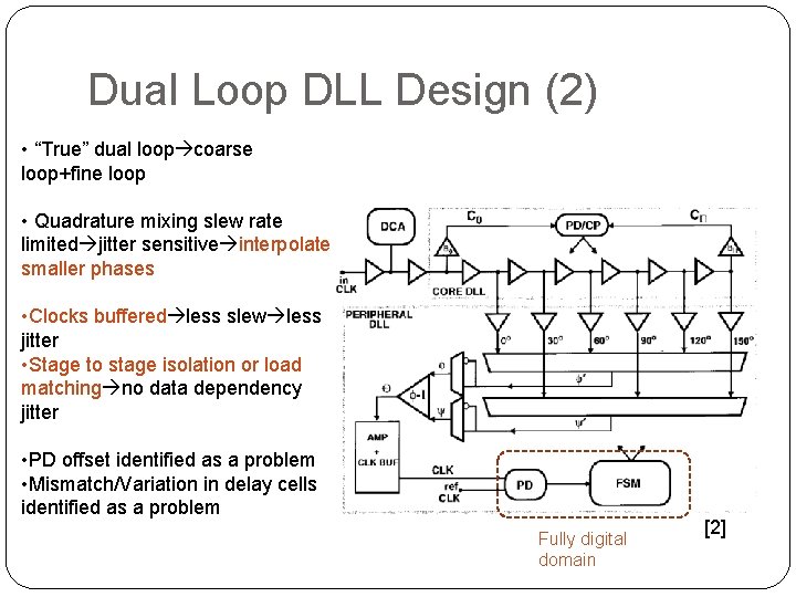
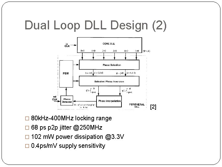
Dual Loop DLL Design (2) • “True” dual loop coarse loop+fine loop • Quadrature mixing slew rate limited jitter sensitive interpolate smaller phases • Clocks buffered less slew less jitter • Stage to stage isolation or load matching no data dependency jitter • PD offset identified as a problem • Mismatch/Variation in delay cells identified as a problem Fully digital domain [2]
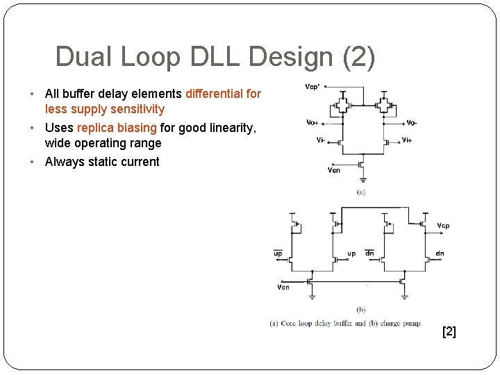
Dual Loop DLL Design (2) • All buffer delay elements differential for less supply sensitivity • Uses replica biasing for good linearity, wide operating range • Always static current [2]
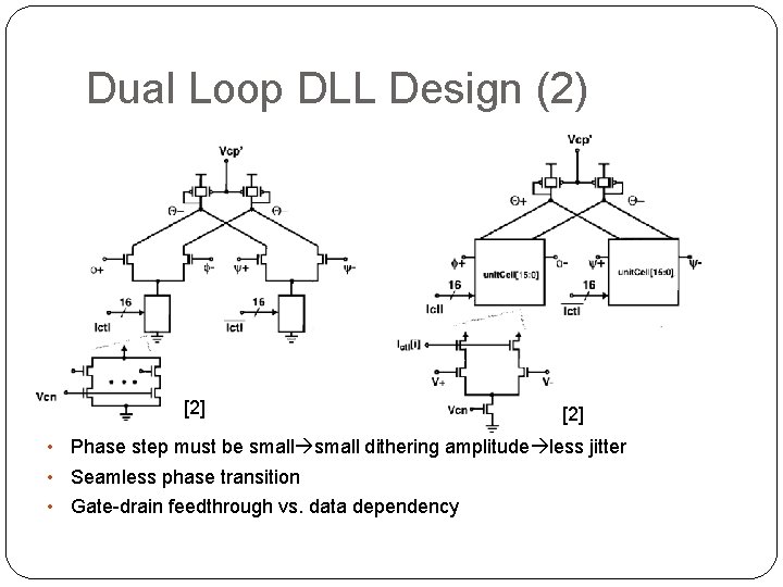
Dual Loop DLL Design (2) [2] • Phase step must be small dithering amplitude less jitter • Seamless phase transition • Gate-drain feedthrough vs. data dependency
Dual Loop DLL Design (2) [2] � 80 k. Hz-400 MHz locking range � 68 ps p 2 p jitter @250 MHz � 102 m. W power dissipation @3. 3 V � 0. 4 ps/m. V supply sensitivity
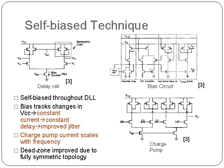
Self-biased Technique Delay cell [3] Bias Circuit � Self-biased throughout DLL � Bias tracks changes in Vcc constant current constant delay improved jitter � Charge pump current scales with frequency � Dead-zone improved due to fully symmetric topology Charge Pump [3]
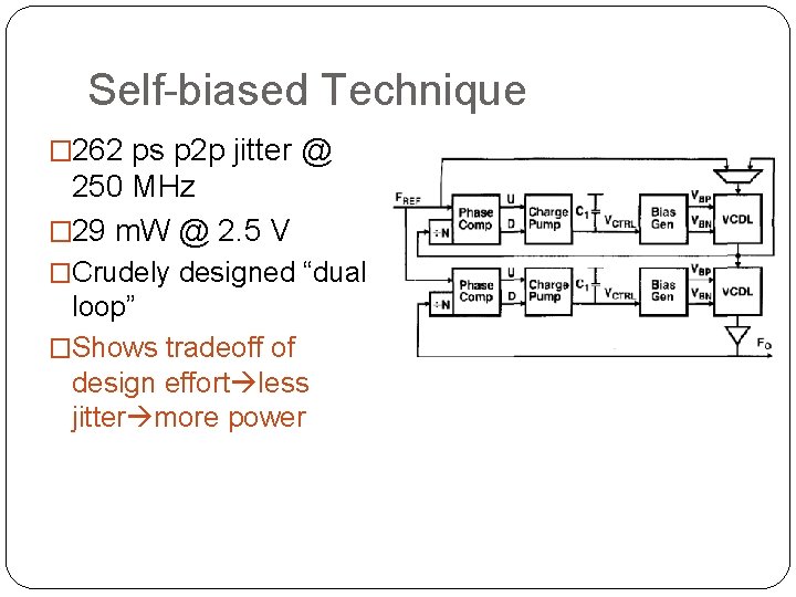
Self-biased Technique � 262 ps p 2 p jitter @ 250 MHz � 29 m. W @ 2. 5 V �Crudely designed “dual loop” �Shows tradeoff of design effort less jitter more power
Outline � DLL Quick Review � Seminal Papers � First “dual loop” with infinite phase capture range � First true dual loop architecture � Summary of DLL Design Issues � A Walk Through Time � The first all digital DLL (1999) � The first mixed mode DLL (1999) � Process variation problem � False lock problem � Fast lock acquisition � PFD jitter � CP jitter � Summary of DLL Design Space � Discussion Questions
Summary of DLL Design � Metrics of interest include: �P 2 p jitter �Power �Supply sensitivity �Operating range �Acquisition time � Sources of jitter include: �Supply/substrate induced �Reference feedthrough �Digital control resolution �Delay line resolution �Phase mixer capabilities �Vcont dithering � Design issues include: � Jitter reduction in VCDL � PD accuracy and speed � CP current balance � Digital integration � Harmonic locking and startup � Duty cycle correction � Process variation control � Fast lock acquisition
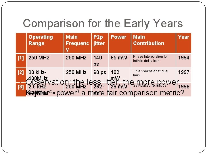
Comparison for the Early Years Operating Range Main P 2 p Frequenc jitter y Power Main Contribution Year [1] 250 MHz 140 ps 65 m. W Phase Interpolation for infinite delay lock 1994 [2] 80 k. Hz 400 MHz 250 MHz 68 ps 102 m. W True “coarse-fine” dual loop 1997 �Observation: the less jitter, the. Self-biased moretechnique power [3] 2. 5 k. Hz 250 MHz 262 400 MHz α×powerβ a more ps �K=jitter 29 m. W 1996 fair comparison metric?
Outline � DLL Quick Review � Seminal Papers � First “dual loop” with infinite phase capture range � First true dual loop architecture � Summary of DLL Design Issues � A Walk Through Time � The first all digital DLL (1999) � The first mixed mode DLL (1999) � Process variation problem � False lock problem � Fast lock acquisition � PFD jitter � CP jitter � Summary of DLL Design Space � Discussion Questions
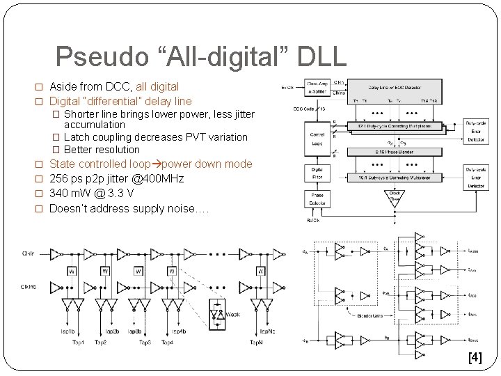
Pseudo “All-digital” DLL � Aside from DCC, all digital � Digital “differential” delay line � Shorter line brings lower power, less jitter accumulation � Latch coupling decreases PVT variation � Better resolution � State controlled loop power down mode � 256 ps p 2 p jitter @400 MHz � 340 m. W @ 3. 3 V � Doesn’t address supply noise…. [4]
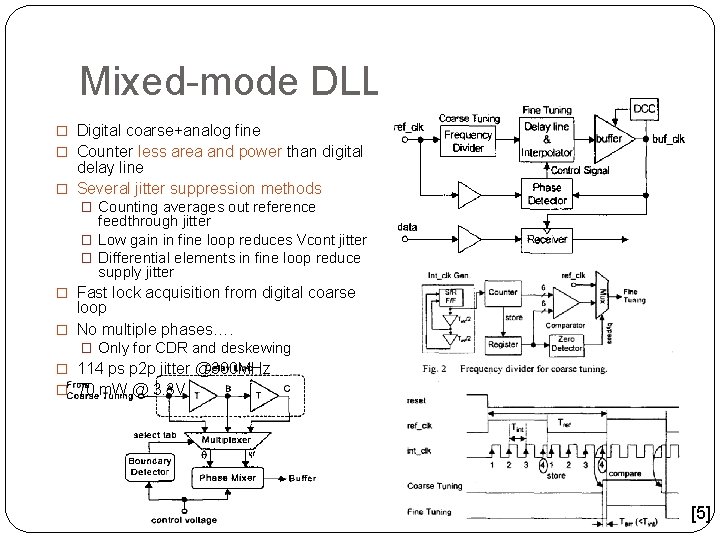
Mixed-mode DLL � Digital coarse+analog fine � Counter less area and power than digital delay line � Several jitter suppression methods � Counting averages out reference feedthrough jitter � Low gain in fine loop reduces Vcont jitter � Differential elements in fine loop reduce supply jitter � Fast lock acquisition from digital coarse loop � No multiple phases…. � Only for CDR and deskewing � 114 ps p 2 p jitter @300 MHz � 70 m. W @ 3. 3 V [5]
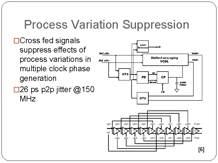
Process Variation Suppression �Cross fed signals suppress effects of process variations in multiple clock phase generation � 26 ps p 2 p jitter @150 MHz [6]
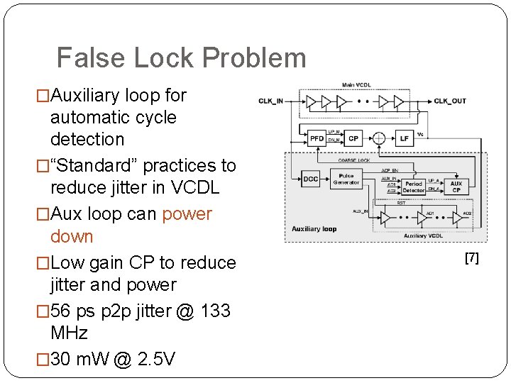
False Lock Problem �Auxiliary loop for automatic cycle detection �“Standard” practices to reduce jitter in VCDL �Aux loop can power down �Low gain CP to reduce jitter and power � 56 ps p 2 p jitter @ 133 MHz � 30 m. W @ 2. 5 V [7]
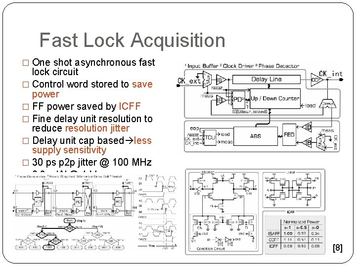
Fast Lock Acquisition � One shot asynchronous fast lock circuit � Control word stored to save power � FF power saved by ICFF � Fine delay unit resolution to reduce resolution jitter � Delay unit cap based less supply sensitivity � 30 ps p 2 p jitter @ 100 MHz � 0. 3 m. W @ 1 V [8]
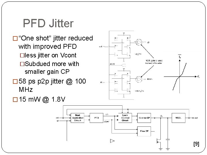
PFD Jitter � “One shot” jitter reduced with improved PFD �less jitter on Vcont �Subdued more with smaller gain CP � 58 ps p 2 p jitter @ 100 MHz � 15 m. W @ 1. 8 V [9]
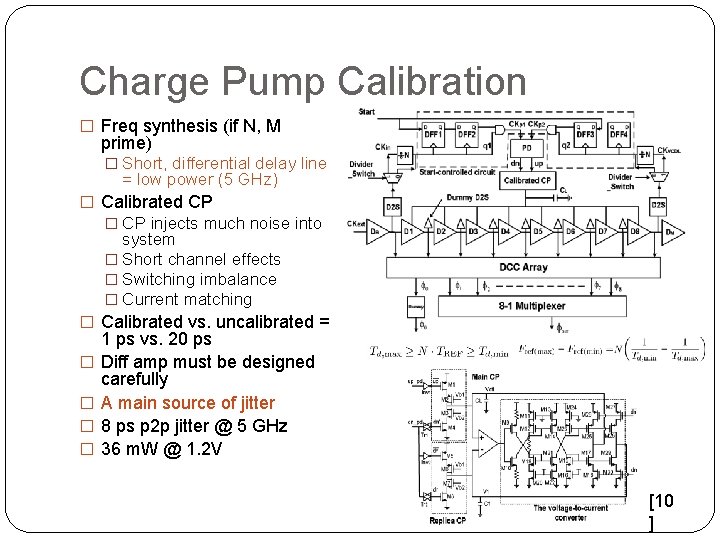
Charge Pump Calibration � Freq synthesis (if N, M prime) � Short, differential delay line = low power (5 GHz) � Calibrated CP � CP injects much noise into system � Short channel effects � Switching imbalance � Current matching � Calibrated vs. uncalibrated = � � 1 ps vs. 20 ps Diff amp must be designed carefully A main source of jitter 8 ps p 2 p jitter @ 5 GHz 36 m. W @ 1. 2 V [10 ]
Outline � DLL Quick Review � Seminal Papers � First “dual loop” with infinite phase capture range � First true dual loop architecture � Summary of DLL Design Issues � A Walk Through Time � The first all digital DLL (1999) � The first mixed mode DLL (1999) � Process variation problem � False lock problem � Fast lock acquisition � PFD jitter � CP jitter � Summary of DLL Design Space � Discussion Questions
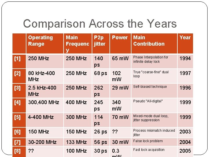
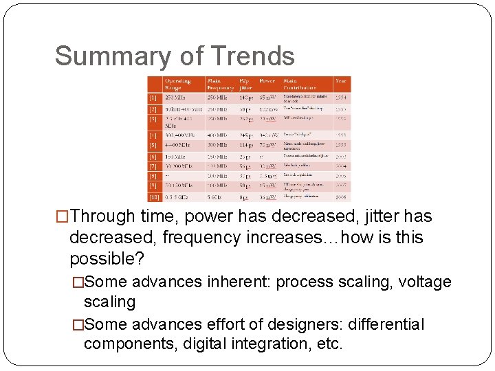
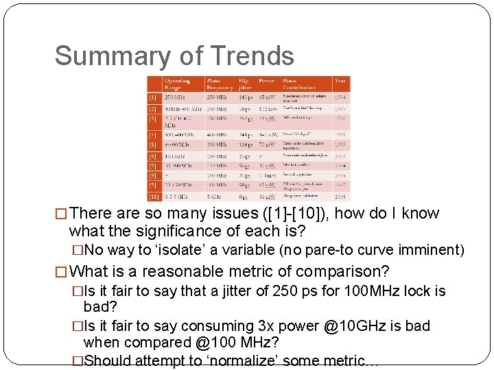
Comparison Across the Years Operating Range Main P 2 p Frequenc jitter y Power Main Contribution Year [1] 250 MHz 140 ps 65 m. W Phase Interpolation for infinite delay lock 1994 [2] 80 k. Hz-400 MHz 250 MHz 68 ps 102 m. W True “coarse-fine” dual loop 1997 [3] 2. 5 k. Hz-400 MHz 250 MHz 262 ps 29 m. W Self-biased technique 1996 [4] 300, 400 MHz 245 ps 340 m. W Pseudo “All-digital” 1999 [5] 4 -400 MHz 300 MHz 114 ps 70 m. W Mixed-mode dual loop, jitter suppression 1999 [6] 150 MHz 26 ps ? ? Process mismatch induced jitter 2003 [7] 30 -200 MHz 133 MHz 56 ps 30 m. W False lock problem 2004 [8] ? ? 100 MHz 30 ps 0. 3 Fast lock acquisition 2005
Summary of Trends �Through time, power has decreased, jitter has decreased, frequency increases…how is this possible? �Some advances inherent: process scaling, voltage scaling �Some advances effort of designers: differential components, digital integration, etc.
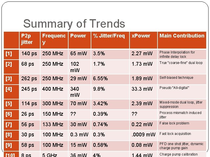
Summary of Trends � There are so many issues ([1]-[10]), how do I know what the significance of each is? �No way to ‘isolate’ a variable (no pare-to curve imminent) � What is a reasonable metric of comparison? �Is it fair to say that a jitter of 250 ps for 100 MHz lock is bad? �Is it fair to say consuming 3 x power @10 GHz is bad when compared @100 MHz? �Should attempt to ‘normalize’ some metric…
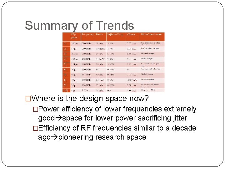
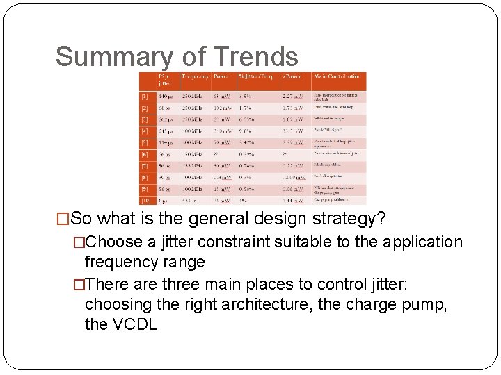
Summary of Trends P 2 p jitter Frequenc Power y % Jitter/Freq x. Power Main Contribution [1] 140 ps 250 MHz 65 m. W 3. 5% 2. 27 m. W Phase Interpolation for infinite delay lock [2] 68 ps 102 m. W 1. 7% 1. 73 m. W True “coarse-fine” dual loop [3] 262 ps 250 MHz 29 m. W 6. 55% 1. 89 m. W Self-biased technique [4] 245 ps 400 MHz 340 m. W 9. 8% 33. 3 m. W Pseudo “All-digital” [5] 114 ps 300 MHz 70 m. W 3. 42% 2. 39 m. W Mixed-mode dual loop, jitter suppression [6] 26 ps 150 MHz ? ? 0. 39% ? ? Process mismatch induced jitter [7] 56 ps 133 MHz 30 m. W 0. 74% 0. 22 m. W False lock problem [8] 30 ps 100 MHz 0. 3 m. W 0. 3% . 0009 m. W Fast lock acquisition [9] 58 ps 100 MHz 15 m. W 0. 08 m. W PFD one shot jitter, dynamic charge pump gain 250 MHz 0. 58% Charge pump calibration
Summary of Trends �Where is the design space now? �Power efficiency of lower frequencies extremely good space for lower power sacrificing jitter �Efficiency of RF frequencies similar to a decade ago pioneering research space
Summary of Trends �So what is the general design strategy? �Choose a jitter constraint suitable to the application frequency range �There are three main places to control jitter: choosing the right architecture, the charge pump, the VCDL
Outline � DLL Quick Review � Seminal Papers � First “dual loop” with infinite phase capture range � First true dual loop architecture � Summary of DLL Design Issues � A Walk Through Time � The first all digital DLL (1999) � The first mixed mode DLL (1999) � Process variation problem � False lock problem � Fast lock acquisition � PFD jitter � CP jitter � Summary of DLL Design Space � Discussion Questions
Discussion Questions �What are the assumptions made on the reference clock? �What are some of the sources of noise? �Why is duty cycle important? �Which blocks are the most important? Think in terms of: power consumption, jitter suppression. �How far can digital integration go? Which applications are suitable for digital DLLs?