Create DLL circuit and Multiple frequency with VHDL


")


- Slides: 25
全新架構的全數位式無類比鎖相倍頻電路 Create DLL circuit and Multiple frequency with VHDL or VERILOG in CPLD, FPGA or ASIC 授課教授 : 陳永耀 博士 學生 : 藍浩濤 P 90921001 電機所控制組
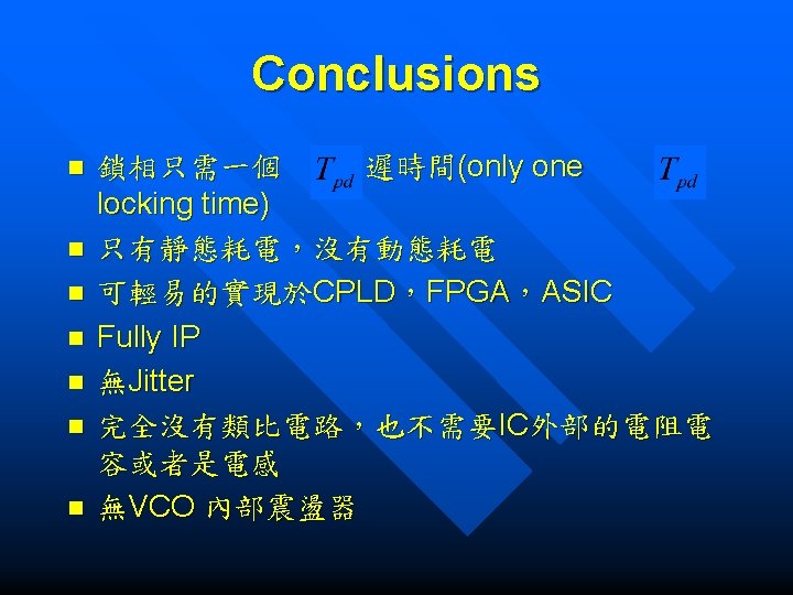
OUTLINE Abstract n Purposes of DLL n DLL Definition and Principle n Circuit Design with VHDL in CPLD and FPGA Flowchart n Simulation Wave for Lattice CPLD n Experimental Results on Oscilloscope n n Conclusions
Abstract § DLL usually implements with logic and analog circuit in ASIC design. § CPLD and FPGA are logic devices, and must design DLL or PLL to implement in devices design first. § Could we create a simple DLL circuit with VHDL or Verilog implementing in CPLD, FPGA or ASIC ?
Purposes of DLL § § § § ADC and DAC CPU design Single chip design SOC design DDR design Wireless circuit DSP
DLL definition and principle § DLL ( Delay Lock Loop )
Circuit design with VHDL in CPLD and FPGA Flowchart Language Description RTL ( Register Transfer Level) Transfer to RTL format Cell Mapping Optimal circuit Netlist of circuit Auto Compiler Flow in CPLD and FPGA
Simulation Waves for Lattice CPLD Lattice 2032 VE-110 n Lattice 2064 VE-100 n Lattice M 4 A 3 -256/100 n Altera EPM 7032 LC 44 -6 n
Lattice 2032 VE-110
Lattice 2032 VE-110
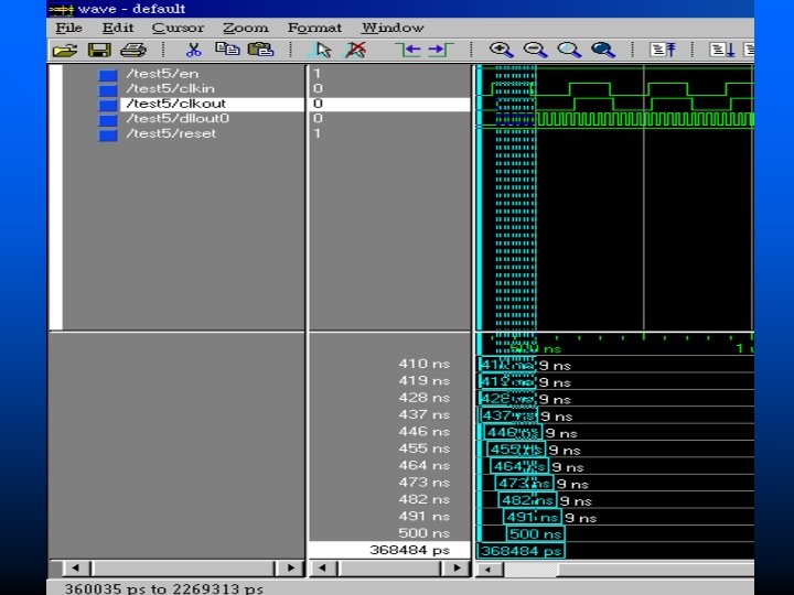
Lattice 2064 VE-100
Lattice M 4 A 3 -256/100
Altera EPM 7032 LC 44 -6
Experimental Results on Oscilloscope Lattice M 4 A 3 -256/160 -10 YC 及電路板實際外觀
Lattice 2064 VE-100 LT 100 及電路板實際外觀
Lattice M 4 A 3 -256/160 -10 YC 延遲的輸出波形
Lattice M 4 A 3 -256/160 -10 YC 倍頻的輸出波形
Lattice 2064 VE-100 LT 100 鎖相的輸出波形
Lattice 2064 VE-100 LT 100 鎖相的輸出波形
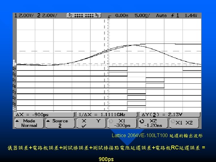
Lattice 2064 VE-100 LT 100 延遲的輸出波形
Lattice 2064 VE-100 LT 100 鎖相的輸出波形
Lattice 2064 VE-100 LT 100 鎖相的輸出波形
Lattice 2064 VE-100 LT 100 倍頻的輸出波形