Phase Locked Loop Design for Transmitting and Receiving

![REFERENCES : [1] Behzad Razavi, “Design of Analog CMOS Integrated Circuits”, Tata-Mc. Graw Hill REFERENCES : [1] Behzad Razavi, “Design of Analog CMOS Integrated Circuits”, Tata-Mc. Graw Hill](https://slidetodoc.com/presentation_image_h/9f93745b177daae0d4b210219abfc0d3/image-32.jpg)

- Slides: 33

Phase Locked Loop Design for Transmitting and Receiving Sections in Optical Wireless Access PRESENTED BY : GUIDED BY: Prof. DEBASIS BEHERA SITANSHU PATI SUBHRANSU SEKHAR NAYAK RAJESH KUMAR MUDULI SUMAN PANI

CONTENTS : 1. Project Framework 2. Introduction 3. Fundamentals of PHASE LOCKED LOOP 4. Basic components of PHASE LOCKED LOOP 5. Response of PLL 6. Implementation in optical access 7. Future work 8. References 2

WHY THIS PROJECT 3 3

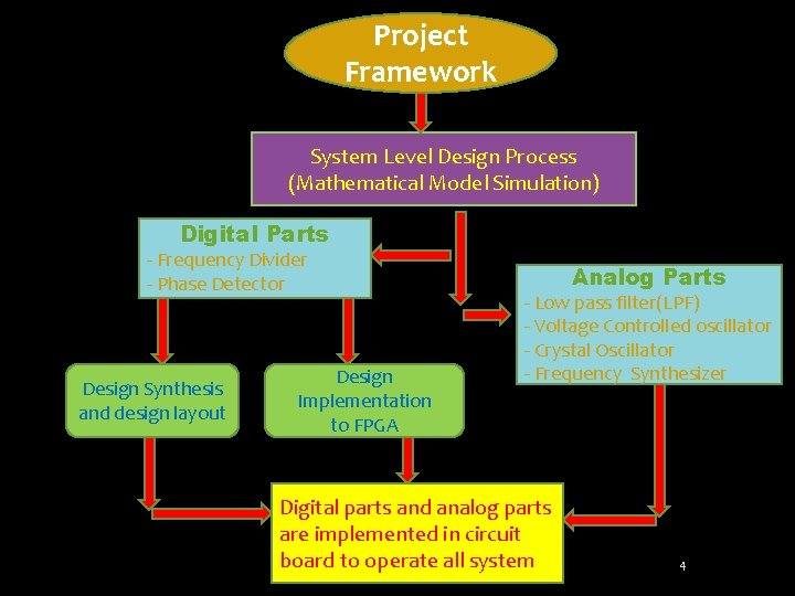
Project Framework System Level Design Process (Mathematical Model Simulation) Digital Parts - Frequency Divider - Phase Detector Design Synthesis and design layout Design Implementation to FPGA Analog Parts - Low pass filter(LPF) - Voltage Controlled oscillator - Crystal Oscillator - Frequency Synthesizer Digital parts and analog parts are implemented in circuit board to operate all system 4

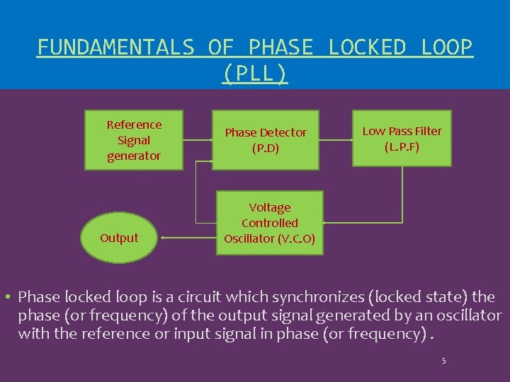
FUNDAMENTALS OF PHASE LOCKED LOOP (PLL) Reference Signal generator Output Phase Detector (P. D) Low Pass Filter (L. P. F) Voltage Controlled Oscillator (V. C. O) • Phase locked loop is a circuit which synchronizes (locked state) the phase (or frequency) of the output signal generated by an oscillator with the reference or input signal in phase (or frequency). 5

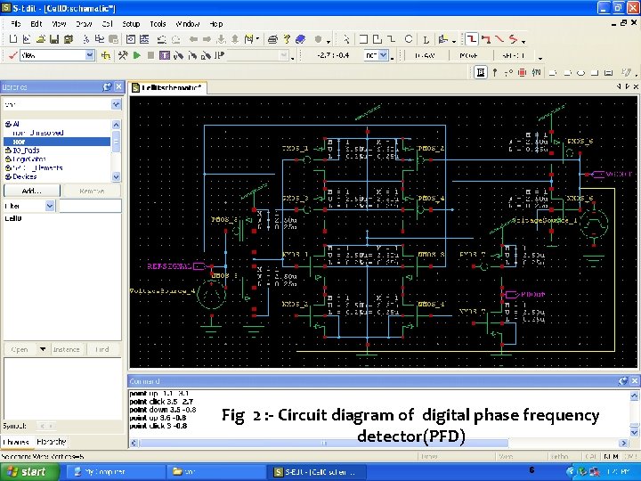
Fig 3 : - Circuit diagram of digital phase detector using tanner tools with Fig 2 : - Circuit diagram of digital phase frequency Fig 6 : - Circuit diagram of phase detector reference input and VCO output detector(PFD) Fig 6 : - Circuit diagram of phase detector 6 6

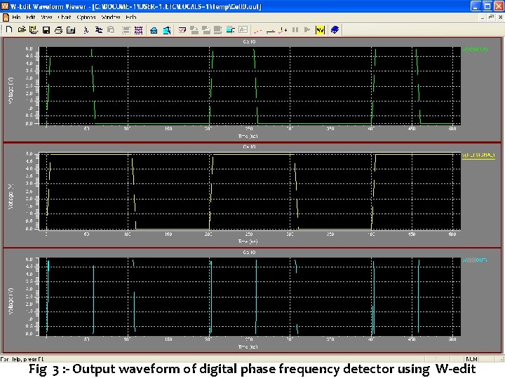
7 Fig 3 : - Output waveform of digital phase frequency detector using W-edit

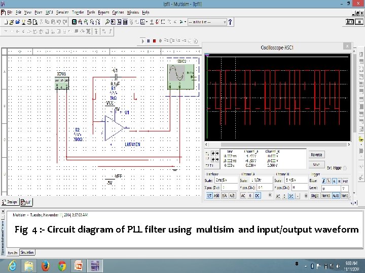
Fig 4 : - Circuit diagram of PLL filter using multisim and input/output waveform 8

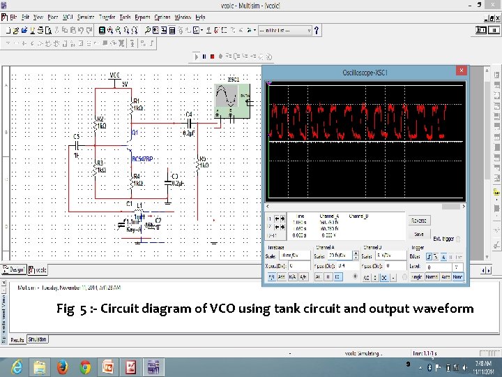
Fig 5 : - Circuit diagram of VCO using tank circuit and output waveform 9 9

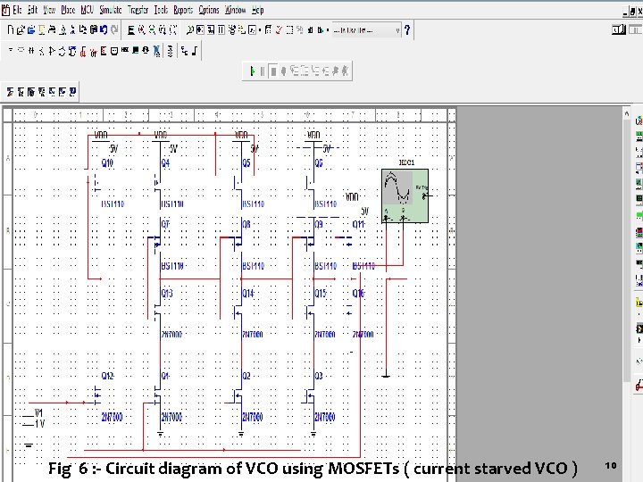
Fig 6 : - Circuit diagram of VCO using MOSFETs ( current starved VCO ) 10 10

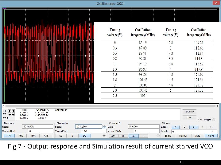
Fig 7 - Output response and Simulation result of current starved VCO 11

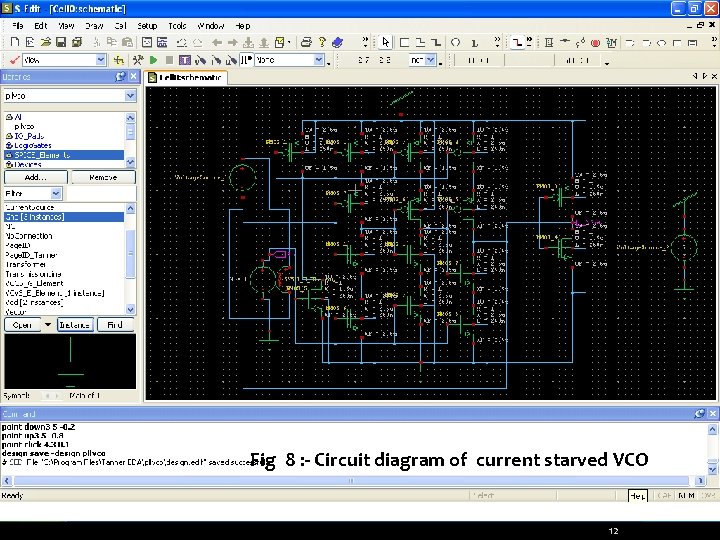
Fig 8 : - Circuit diagram of current starved VCO 12

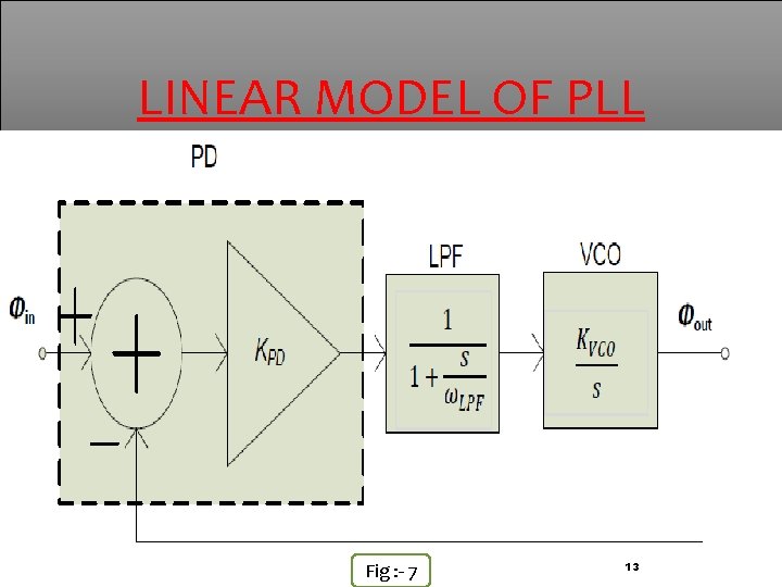
LINEAR MODEL OF PLL Fig : - 7 13

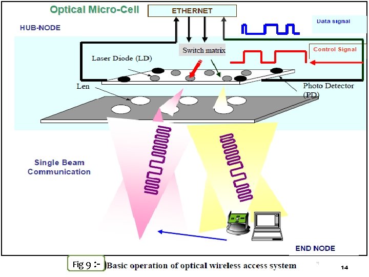
Fig 9 : - 14 14

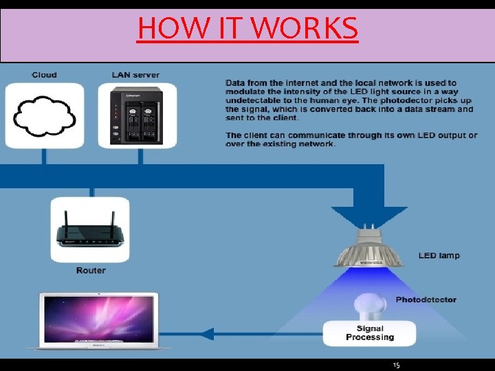
HOW IT WORKS 15

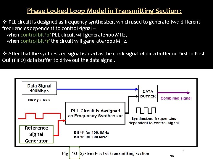
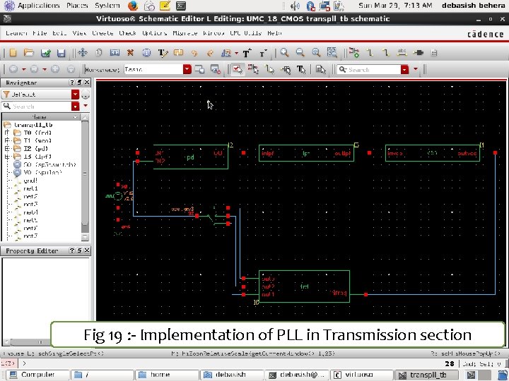
Phase Locked Loop Model in Transmitting Section : v PLL circuit is designed as frequency synthesizer, which used to generate two different frequencies dependent to control signal – when control bit ‘ 0’ PLL circuit will generate 100 MHz, when control bit ‘ 1’ the circuit will generate 100. 1 MHz. v After that the synthesized signal is used as the clock signal of data buffer or First-In First. Out (FIFO) data buffer to drive out the data signal. Reference Signal Generator 10 16 16

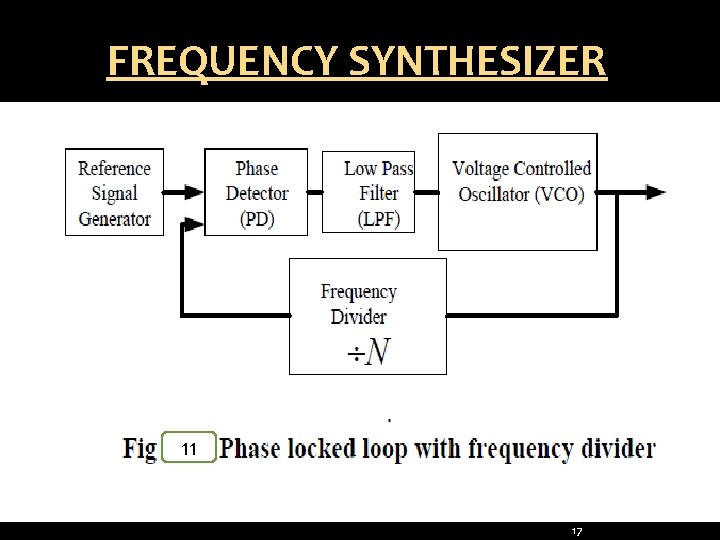
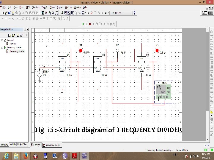
FREQUENCY SYNTHESIZER 11 17

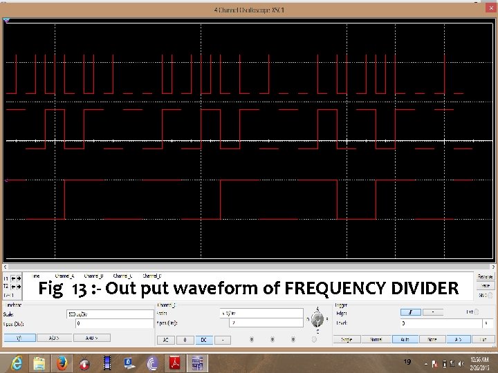
Fig 12 : - Circuit diagram of FREQUENCY DIVIDER 18 18

Fig 13 : - Out put waveform of FREQUENCY DIVIDER 19

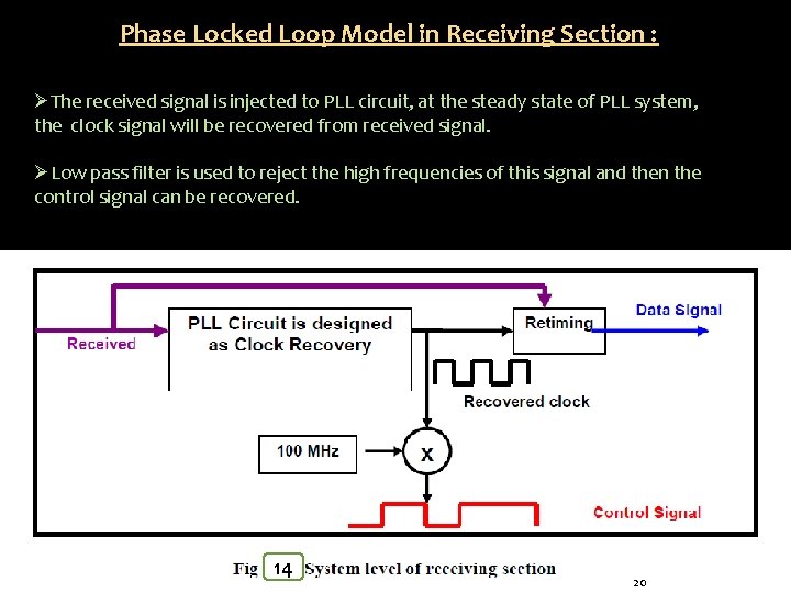
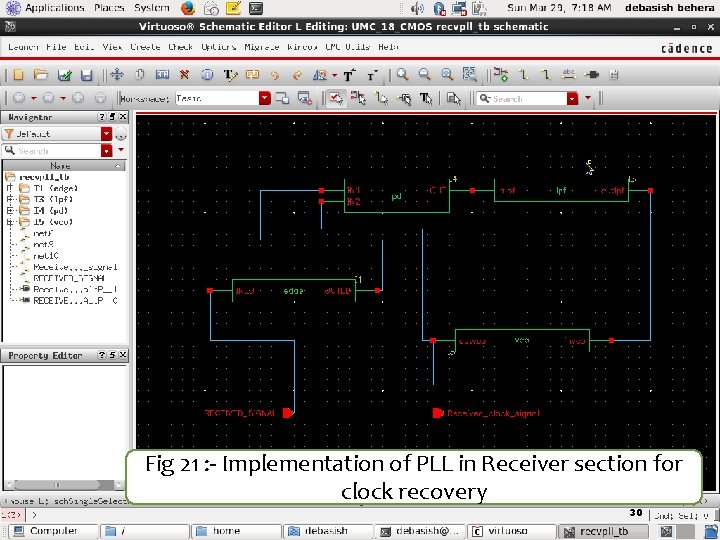
Phase Locked Loop Model in Receiving Section : ØThe received signal is injected to PLL circuit, at the steady state of PLL system, the clock signal will be recovered from received signal. ØLow pass filter is used to reject the high frequencies of this signal and then the control signal can be recovered. 14 20

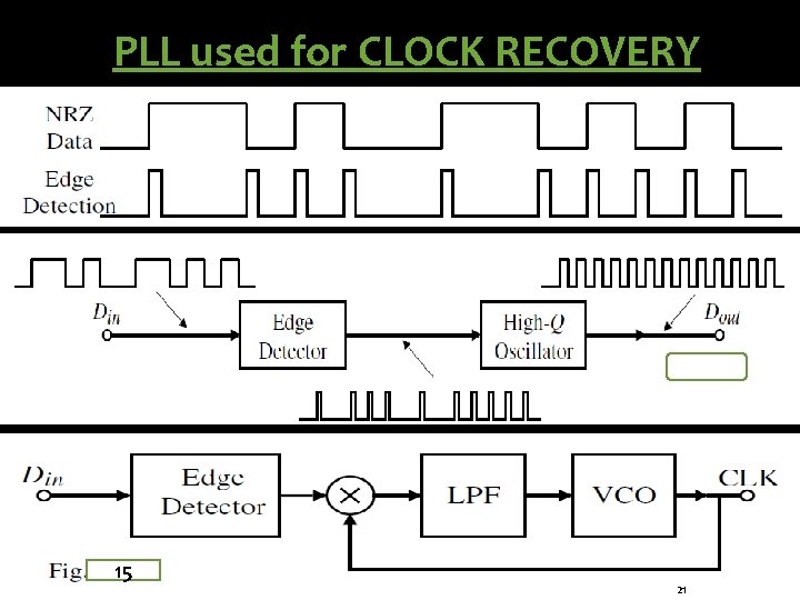
PLL used for CLOCK RECOVERY 15 21

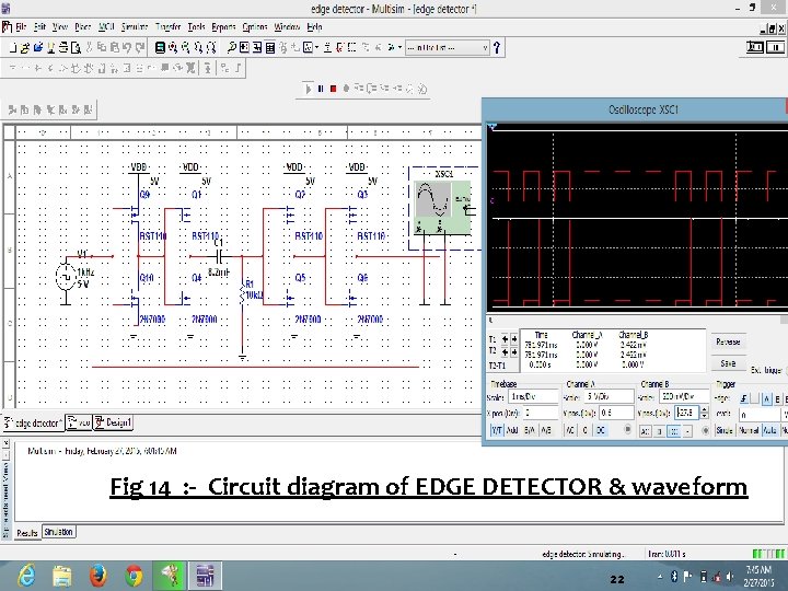
Fig 14 : - Circuit diagram of EDGE DETECTOR & waveform 22 22

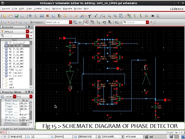
Fig 15 : - SCHEMATIC DIAGRAM OF PHASE DETECTOR 23 23

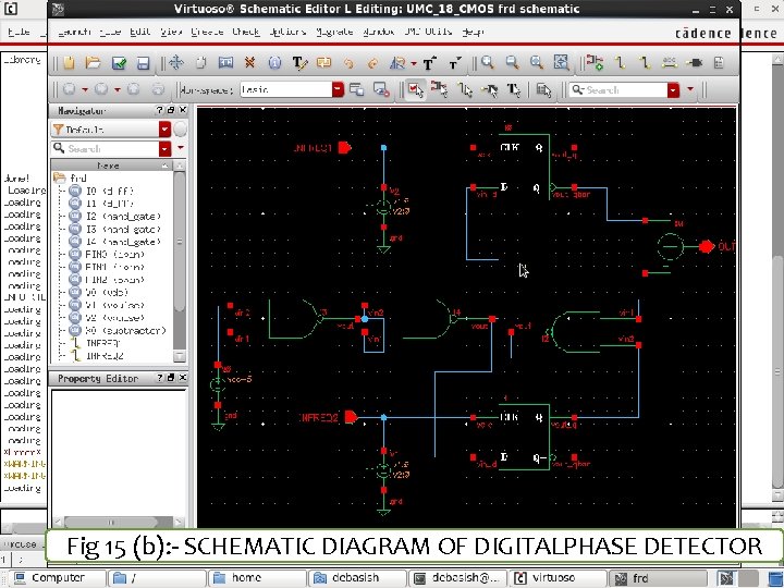
Fig 15 (b): - SCHEMATIC DIAGRAM OF DIGITALPHASE DETECTOR 24

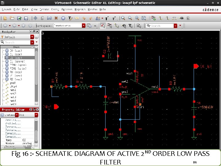
Fig 16 : - SCHEMATIC DIAGRAM OF ACTIVE 2 ND ORDER LOW PASS FILTER 25

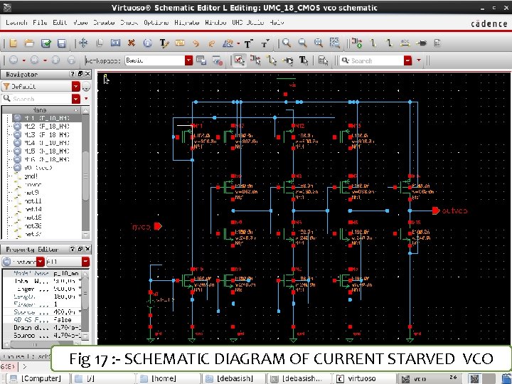
Fig 17 : - SCHEMATIC DIAGRAM OF CURRENT STARVED VCO 26 26

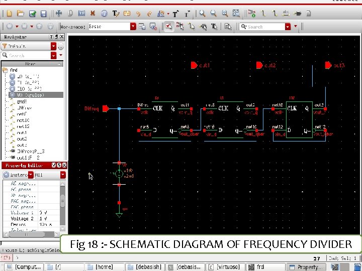
Fig 18 : - SCHEMATIC DIAGRAM OF FREQUENCY DIVIDER 27 27 27

Fig 19 : - Implementation of PLL in Transmission section 28 28

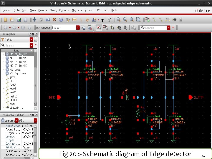
Fig 20 : - Schematic diagram of Edge detector 29 29

Fig 21 : - Implementation of PLL in Receiver section for clock recovery 30 30

1. Future Works Hardware implementation of the project to be done. 2. Working of the project in GHz range by virtue of which more faster application speed can be achieved. 3. Optimization of VCO in accordance with the increased frequency range to achieve more clarity and faster speed in communication. 4. Improvement of output performance in transmitting and receiving section such as : Lock range, Capture range, Pull in time, Bandwidth of PLL. 5. Noise reduction during the communication by varying the system parameters such as : Jitter, Phase noise ( VCO, PD, Frequency Divider), Reference spur. 6. Implementation of the circuit in various environment such as: Airplanes, High profile cars and buses, Communication sectors in factories etc. to view the proper practical applications and modification accordingly. 31
![REFERENCES 1 Behzad Razavi Design of Analog CMOS Integrated Circuits TataMc Graw Hill REFERENCES : [1] Behzad Razavi, “Design of Analog CMOS Integrated Circuits”, Tata-Mc. Graw Hill](https://slidetodoc.com/presentation_image_h/9f93745b177daae0d4b210219abfc0d3/image-32.jpg)
REFERENCES : [1] Behzad Razavi, “Design of Analog CMOS Integrated Circuits”, Tata-Mc. Graw Hill 2002, Ch. 15, page. 532 -576 [2] Swanand Solanke, D. P. Acharya, “Design of Efficient Charge Pump in Phase Locked Loop for Wireless Communication”, National Conference on Emerging Trends in Engineering Technology and Applications, 2009, NCETETA 09. [3] “Li-Fi (Light Fidelity)-The Future Technology In Wireless Communication”, International Journal of Applied Engineering Research, ISSN 0973 -4562 Vol. 7 (2013) [4] Koji Nonaka, Yoshiyuki Isobe, High Speed Optical Wireless Access with VCSELArray Beam Micro-cell System. [5] Vemceslav F. Kroupa, Phase Locked Loops and Frequency Synthesis, John Wiley&Sons Ltd, 2003. [6] Behzad Razavi, Monolithic Phase-Locked Loops and Clock Recovery Circuits, Wiley - Interscience, 2006. [7] “PLL design for optical fiber li-fi” by Ampornrat Posri , February 2005 [8] Dan H. Wolaver, Phased-Locked Loop Circuit Design, Prentice Hall, 1991. [9] Floy M. Gardner, Charge-Pump Phase Locked Loops, IEEE, Trans. November 2010. [10] Wogeun Ree, “Design of High Performance CMOS Charge Pumps in Phase Locked Loop”, IEEE International Symposium on Circuits and Systems ISCAS`99, vol. 2, June 2011. 32 32

33