Piezoelectric MEMS Resonator Measurement and Characterization April 6


- Slides: 32

Piezoelectric MEMS Resonator Measurement and Characterization April 6, 2004 Joung-Mo Kang, David Carter, Doug White, and Amy Duwel The Charles Stark Draper Laboratory DARPA MTO MEMS

Presentation Overview 1. Background and device models 2. Filter design 3. L-Bar measurements 4. Parasitic investigations 5. Conclusion DARPA MTO MEMS

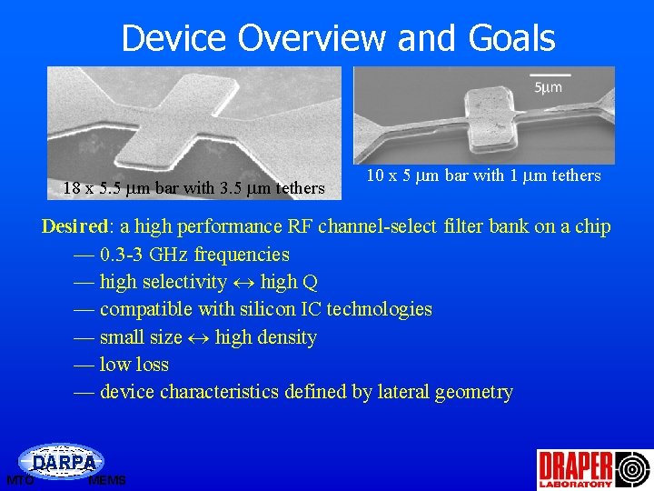
Device Overview and Goals 18 x 5. 5 mm bar with 3. 5 mm tethers 10 x 5 mm bar with 1 mm tethers Desired: a high performance RF channel-select filter bank on a chip — 0. 3 -3 GHz frequencies — high selectivity high Q — compatible with silicon IC technologies — small size high density — low loss — device characteristics defined by lateral geometry DARPA MTO MEMS

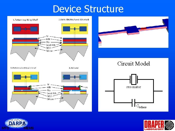
Device Structure Circuit Model resonator Ctethers DARPA MTO MEMS

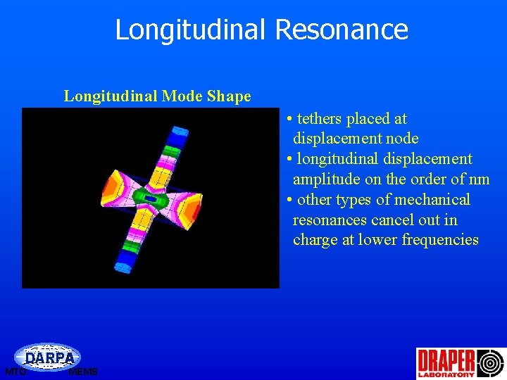
Longitudinal Resonance Longitudinal Mode Shape • tethers placed at displacement node • longitudinal displacement amplitude on the order of nm • other types of mechanical resonances cancel out in charge at lower frequencies DARPA MTO MEMS

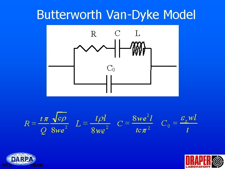
Butterworth Van-Dyke Model C R L C 0 t p cr R= Q 8 we 2 DARPA MTO MEMS tr l L= 8 we 2 8 we 2 l C= tcp 2 C 0 = e z wl t

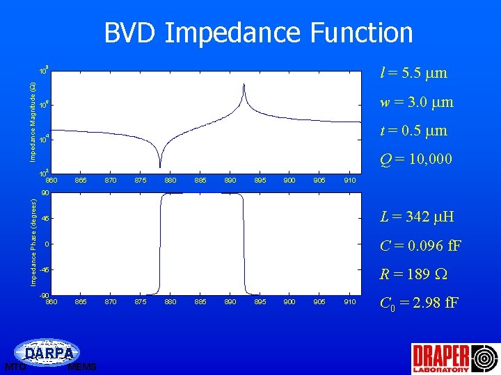
BVD Impedance Function l = 5. 5 mm 8 Impedance Magnitude (W) 10 w = 3. 0 mm 6 10 t = 0. 5 mm 4 10 Q = 10, 000 2 10 865 870 875 880 885 890 895 900 905 910 Impedance Phase (degrees) 90 L = 342 m. H 45 C = 0. 096 f. F 0 R = 189 W -45 -90 865 DARPA MTO MEMS 870 875 880 885 890 895 900 905 910 C 0 = 2. 98 f. F

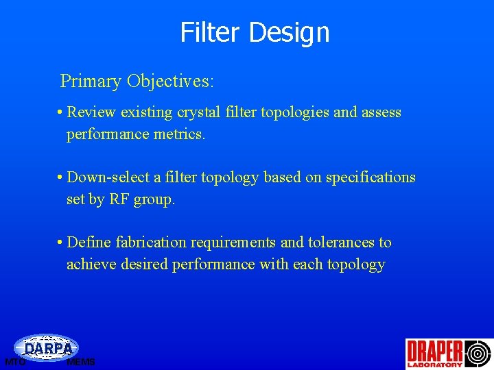
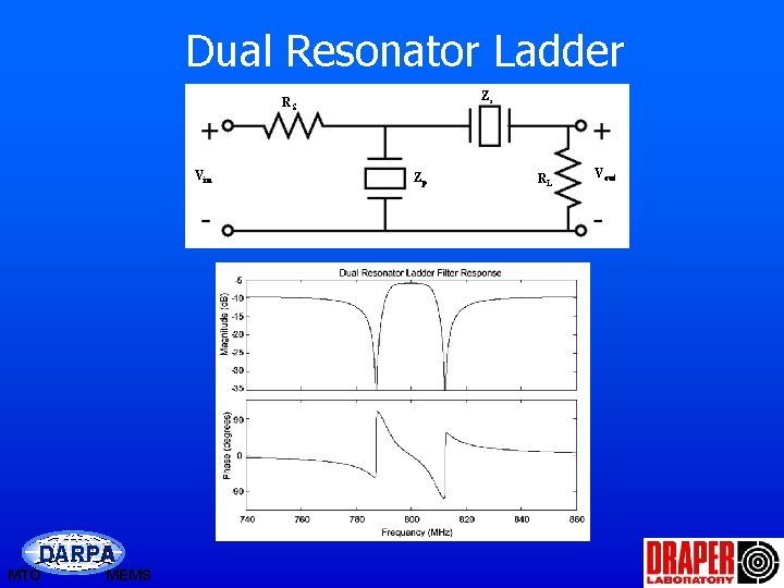
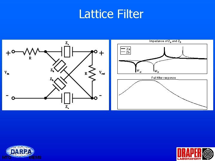
Filter Design Primary Objectives: • Review existing crystal filter topologies and assess performance metrics. • Down-select a filter topology based on specifications set by RF group. • Define fabrication requirements and tolerances to achieve desired performance with each topology DARPA MTO MEMS

Dual Resonator Ladder Zs RS Vin DARPA MTO MEMS Zp RL Vout

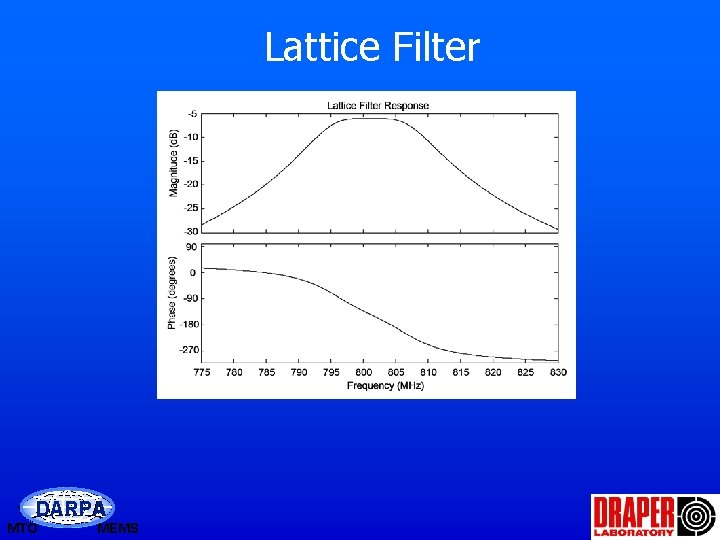
Lattice Filter Impedance of Za and Zb Za Za Zb R Zb Vin R Za MTO MEMS wa wb Full filter response Zb DARPA Vout

Lattice Filter DARPA MTO MEMS

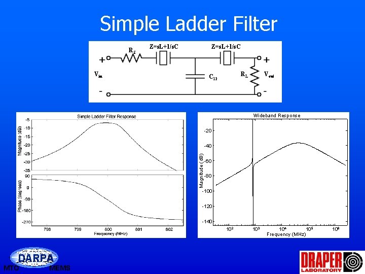
Simple Ladder Filter RS Z=s. L+1/s. C Vin Vout RL C 12 Wideband Response -20 Magnitude (d. B) -40 -60 -80 -100 -120 -140 102 DARPA MTO MEMS 103 104 105 Frequency (MHz) 106

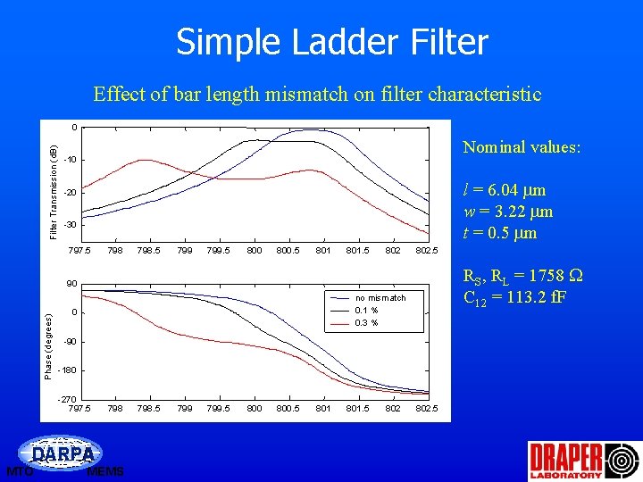
Simple Ladder Filter Effect of bar length mismatch on filter characteristic Filter Transmission (d. B) 0 Nominal values: -10 l = 6. 04 mm w = 3. 22 mm t = 0. 5 mm -20 -30 797. 5 798. 5 799. 5 800. 5 801. 5 802. 5 RS, RL = 1758 W C 12 = 113. 2 f. F Phase (degrees) 90 no mismatch data 1 0. 1 % data 2 0. 3 % data 3 0 -90 -180 -270 797. 5 DARPA MTO 798 MEMS 798. 5 799. 5 800. 5 801. 5 802. 5

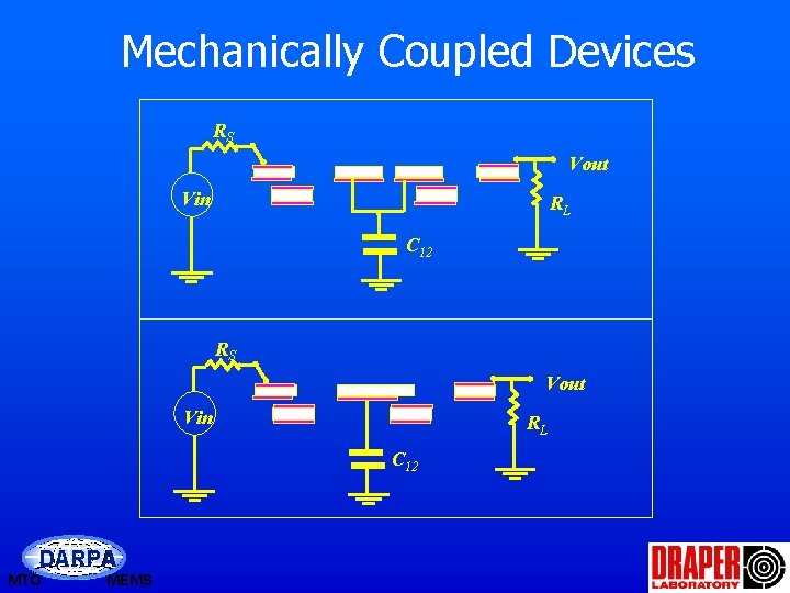
Mechanically Coupled Devices RS Vout Vin RL C 12 DARPA MTO MEMS

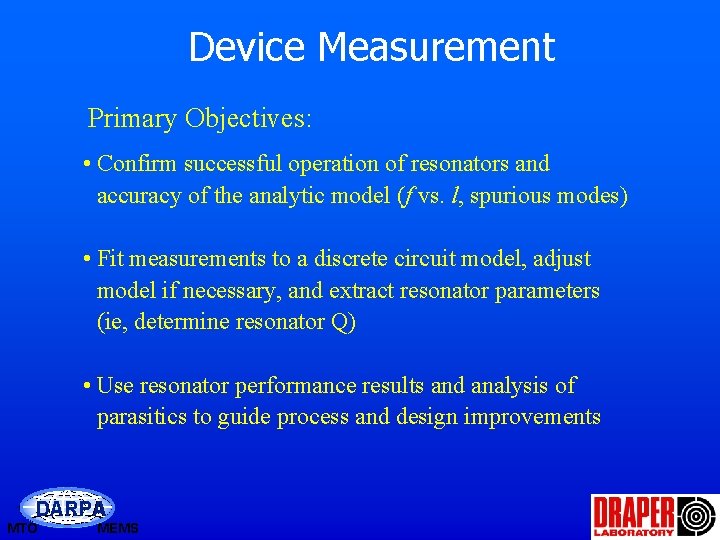
Device Measurement Primary Objectives: • Confirm successful operation of resonators and accuracy of the analytic model (f vs. l, spurious modes) • Fit measurements to a discrete circuit model, adjust model if necessary, and extract resonator parameters (ie, determine resonator Q) • Use resonator performance results and analysis of parasitics to guide process and design improvements DARPA MTO MEMS

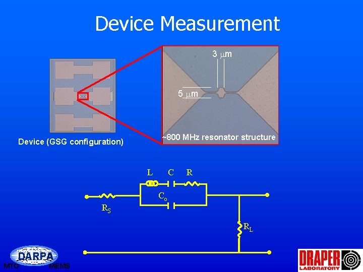
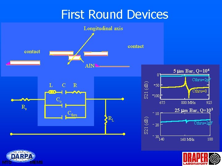
Device Measurement 3 mm 5 mm ~800 MHz resonator structure Device (GSG configuration) L C R Co RS RL DARPA MTO MEMS

First Round Devices Longitudinal axis contact Al. N 5 mm Bar, Q=104 C R Co Rs Cthru=2 p. F 50 Cthru=0 100 675 Cthru RL 10 S 21 (d. B) L S 21 (d. B) 0 20 30 140 DARPA MTO MEMS 800 MHz 925 25 mm Bar, Q=103 Cthru=2 p. F 160 MHz 180

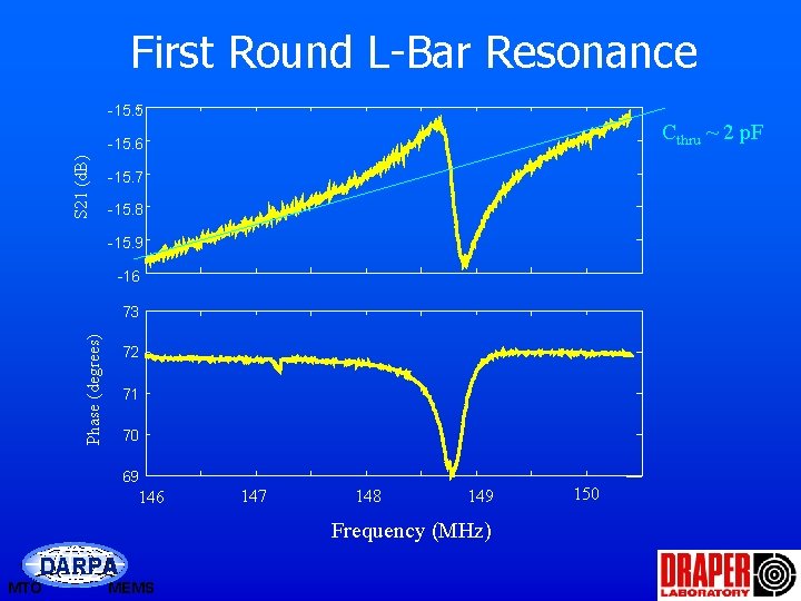
First Round L-Bar Resonance -15. 5 Cthru ~ 2 p. F S 21 (d. B) -15. 6 -15. 7 -15. 8 -15. 9 -16 Phase (degrees) 73 72 71 70 69 146 147 148 149 Frequency (MHz) DARPA MTO MEMS 150

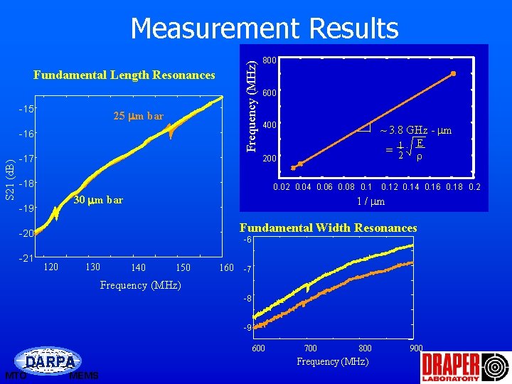
Fundamental Length Resonances -15 25 mm bar S 21 (d. B) -16 Frequency (MHz) Measurement Results -17 800 600 400 = 12 200 -18 0. 02 0. 04 0. 06 0. 08 0. 1 30 mm bar -19 × E r 0. 12 0. 14 0. 16 0. 18 0. 2 1 / mm Fundamental Width Resonances -20 -21 ~ 3. 8 GHz - mm -6 120 130 140 150 160 -7 Frequency (MHz) -8 -9 600 DARPA MTO MEMS 700 800 Frequency (MHz) 900

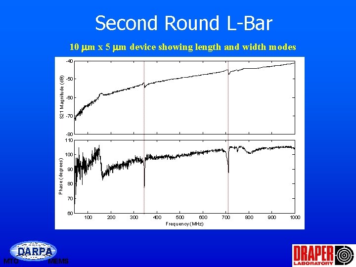
Second Round L-Bar 10 mm x 5 mm device showing length and width modes S 21 Magnitude (d. B) -40 -50 -60 -70 -80 110 Phase (degrees) 100 90 80 70 60 DARPA MTO MEMS 100 200 300 400 500 600 Frequency (MHz) 700 800 900 1000

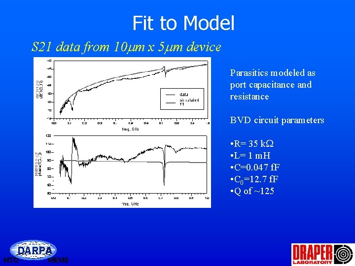
Fit to Model S 21 data from 10 mm x 5 mm device Parasitics modeled as port capacitance and resistance BVD circuit parameters • R= 35 k. W • L= 1 m. H • C=0. 047 f. F • C 0=12. 7 f. F • Q of ~125 DARPA MTO MEMS

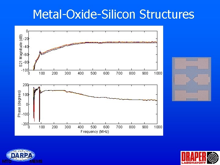
Metal-Oxide-Silicon Structures S 21 Magnitude (d. B) 0 -20 -40 -60 -80 -100 0 100 200 300 400 500 600 700 800 900 100 200 300 400 500 600 Frequency (MHz) 700 800 900 1000 Phase (degrees) 200 100 0 -100 -200 0 DARPA MTO MEMS

Glass Substrate S 21 Magnitude (d. B) OP 6 on Glass -60 OP 6 fit parameters: -80 0 - pure open to ground data simulation -100 500 1000 1500 2000 2500 3000 1500 2000 Frequency (MHz) 2500 3000 Phase (degrees) 150 100 50 0 0 DARPA MTO MEMS - 1. 43 f. F thru capacitance

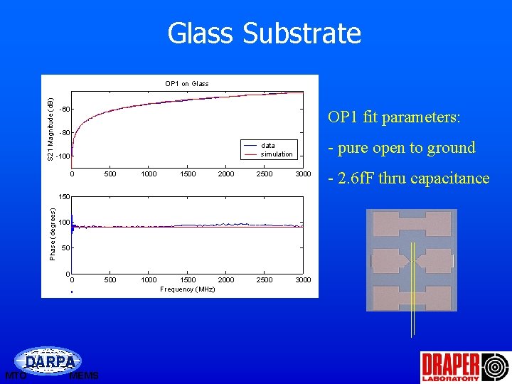
Glass Substrate S 21 Magnitude (d. B) OP 1 on Glass -60 OP 1 fit parameters: -80 -100 0 - pure open to ground data simulation 500 1000 1500 2000 2500 3000 1500 2000 Frequency (MHz) 2500 3000 Phase (degrees) 150 100 50 0 0 DARPA MTO MEMS - 2. 6 f. F thru capacitance

Conclusions • Filter designs will be implemented on upcoming mask layout. Mechanically coupled device will be used. • An accurate model of parasitics is vital for obtaining useful device measurements. • Ongoing work to define explanation for the 100 MHz resonance on silicon substrate, and the wideband phase noise DARPA MTO MEMS

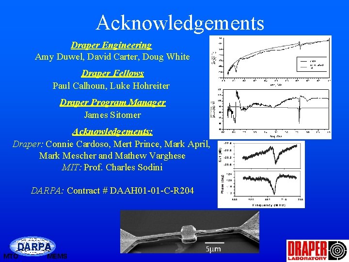
Acknowledgements Draper Engineering Amy Duwel, David Carter, Doug White Draper Fellows Paul Calhoun, Luke Hohreiter Draper Program Manager James Sitomer Acknowledgements: Draper: Connie Cardoso, Mert Prince, Mark April, Mark Mescher and Mathew Varghese MIT: Prof. Charles Sodini DARPA: Contract # DAAH 01 -01 -C-R 204 DARPA MTO MEMS

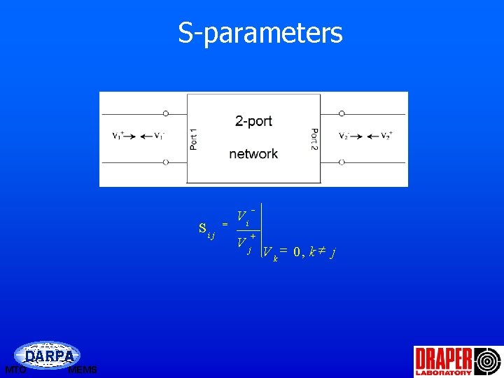
S-parameters Sij DARPA MTO MEMS = Vi - V + j V k = 0, k ¹ j

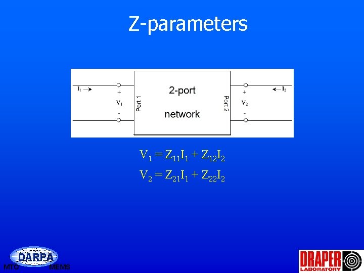
Z-parameters V 1 = Z 11 I 1 + Z 12 I 2 V 2 = Z 21 I 1 + Z 22 I 2 DARPA MTO MEMS

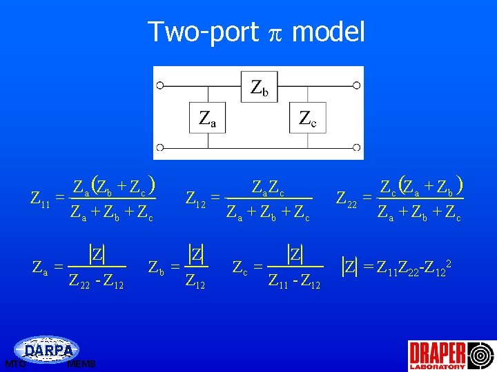
Two-port p model Za (Zb + Zc ) Z 11 = Za + Z b + Zc Za = Z Z 22 - Z 12 DARPA MTO MEMS Zb = Za Zc Z 12 = Za + Z b + Zc Z Z 12 Zc = Z Z 11 - Z 12 Zc (Za + Z b ) Z 22 = Za + Z b + Zc Z = Z 11 Z 22 -Z 122

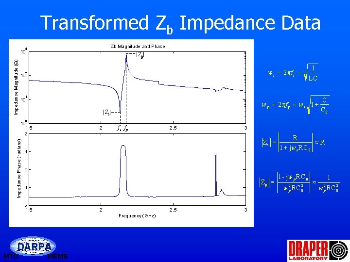
Transformed Zb Impedance Data Zb Magnitude and Phase 3 Impedance Magnitude (W) 10 |Zp| w s = 2 πf s = 2 10 1 LC 1 10 w p = 2 πf p = w s 1 + |Zs| C C 0 0 Impedance Phase (radians) 10 1. 5 2 2 fs fp 3 Zs = 1 R » R 1 + jw s RC 0 0 Zp = -1 -2 1. 5 2 2. 5 Frequency (GHz) DARPA MTO 2. 5 MEMS 3 1 - jw p RC 0 w 2 p RC 02 » 1 w 2 p RC 02

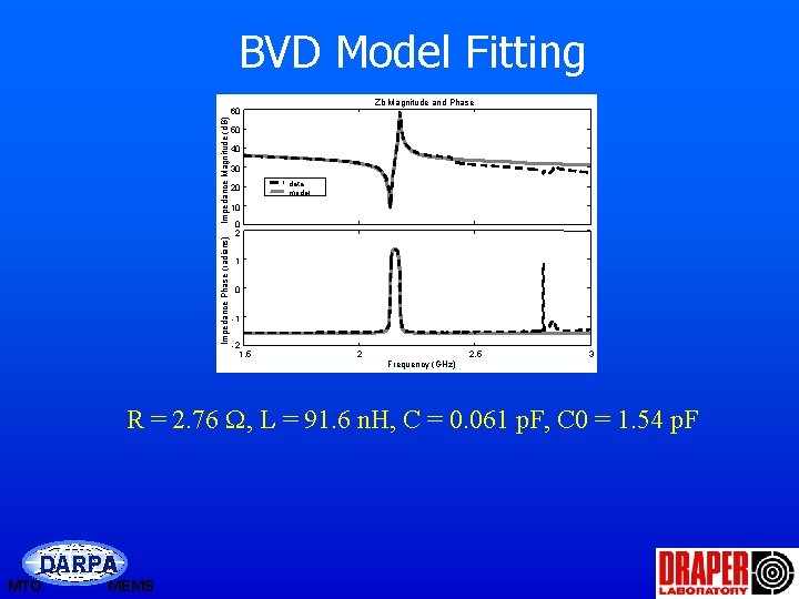
BVD Model Fitting Zb Magnitude and Phase Impedance Phase (radians) Impedance Magnitude (d. B) 60 50 40 30 20 data model 10 0 2 1 0 -1 -2 1. 5 2 2. 5 3 Frequency (GHz) R = 2. 76 W, L = 91. 6 n. H, C = 0. 061 p. F, C 0 = 1. 54 p. F DARPA MTO MEMS

Filter Design Constraints placed on equivalent circuit parameters by bar geometry: • Q assumed to be a function of the process and static • Two degrees of freedom, l and w/t • Resonant frequency fixes l uniquely • For a given frequency, the other degree of freedom controls the “impedance level” • C/C 0 fixed by piezoelectric materials parameters DARPA MTO MEMS