Photonic OnChip Networks for PerformanceEnergy Optimized Off Chip
![Hybrid Circuit-Switched Photonic Network Broadband 1× 2 Switch [Cornell, 2008] Transmission Broadband 2× 2 Hybrid Circuit-Switched Photonic Network Broadband 1× 2 Switch [Cornell, 2008] Transmission Broadband 2× 2](https://slidetodoc.com/presentation_image_h2/be306fc2e68039069be1c53d19fd7185/image-14.jpg)
![Hybrid Circuit-Switched Photonic Network 17 [Bergman, HPEC ’ 07] International Symposium on Networks-on-Chip 9/26/2021 Hybrid Circuit-Switched Photonic Network 17 [Bergman, HPEC ’ 07] International Symposium on Networks-on-Chip 9/26/2021](https://slidetodoc.com/presentation_image_h2/be306fc2e68039069be1c53d19fd7185/image-17.jpg)
- Slides: 29

Photonic On-Chip Networks for Performance-Energy Optimized Off -Chip Memory Access GILBERT HENDRY JOHNNIE CHAN, DANIEL BRUNINA, LUCA CARLONI, KEREN BERGMAN Lightwave Research Laboratory Columbia University New York, NY

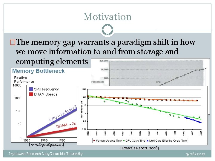
Motivation �The memory gap warrants a paradigm shift in how we move information to and from storage and computing elements [www. Open. Sparc. net] Lightwave Research Lab, Columbia University [Exascale Report, 2008] 9/26/2021

Main Premise �Current memory subsystem technology and packaging are not well-suited to future trends Networks on chip Growing cache sizes Growing bandwidth requirements Growing pin counts Lightwave Research Lab, Columbia University 9/26/2021

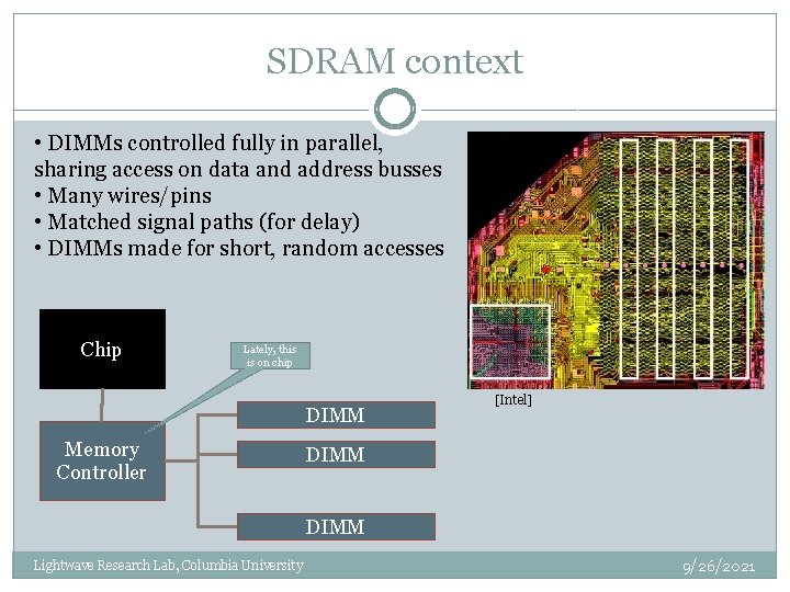
SDRAM context • DIMMs controlled fully in parallel, sharing access on data and address busses • Many wires/pins • Matched signal paths (for delay) • DIMMs made for short, random accesses Chip Lately, this is on chip DIMM Memory Controller [Intel] DIMM Lightwave Research Lab, Columbia University 9/26/2021

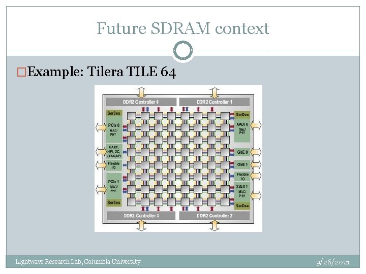
Future SDRAM context �Example: Tilera TILE 64 Lightwave Research Lab, Columbia University 9/26/2021

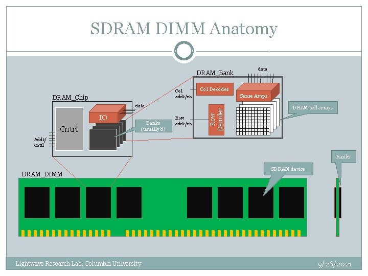
SDRAM DIMM Anatomy DRAM_Bank DRAM_Chip data IO Cntrl Banks (usually 8) Row addr/en Col Decoder Sense Amps Row Decoder Col addr/en data DRAM cell arrays Addr/ cntrl Ranks DRAM_DIMM Lightwave Research Lab, Columbia University SDRAM device 9/26/2021

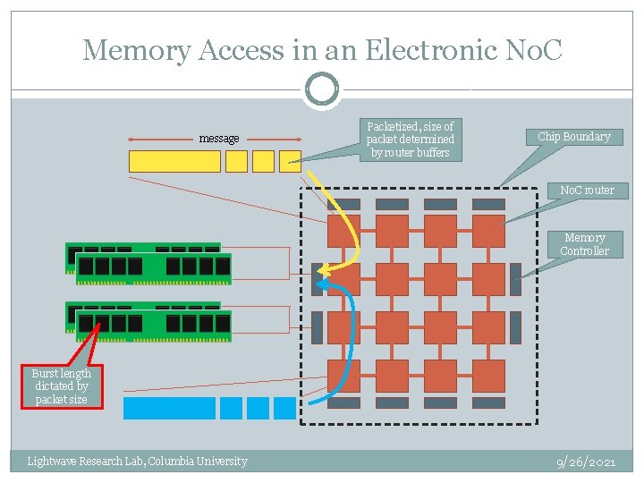
Memory Access in an Electronic No. C message Packetized, size of packet determined by router buffers Chip Boundary No. C router Memory Controller Burst length dictated by packet size Lightwave Research Lab, Columbia University 9/26/2021

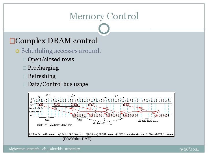
Memory Control �Complex DRAM control Scheduling accesses around: � Open/closed rows � Precharging � Refreshing � Data/Control bus usage [DRAMsim, UMD] Lightwave Research Lab, Columbia University 9/26/2021

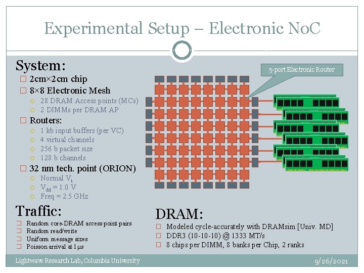
Experimental Setup – Electronic No. C System: 5 -port Electronic Router � 2 cm× 2 cm chip � 8× 8 Electronic Mesh 28 DRAM Access points (MCs) 2 DIMMs per DRAM AP � Routers: 1 kb input buffers (per VC) 4 virtual channels 256 b packet size 128 b channels � 32 nm tech. point (ORION) Normal Vt Vdd = 1. 0 V Freq = 2. 5 GHz Traffic: � � Random core-DRAM access point pairs Random read/write Uniform message sizes Poisson arrival at 1µs Lightwave Research Lab, Columbia University DRAM: � Modeled cycle-accurately with DRAMsim [Univ. MD] � DDR 3 (10 -10 -10) @ 1333 MT/s � 8 chips per DIMM, 8 banks per Chip, 2 ranks 9/26/2021

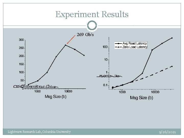
Experiment Results 269 Gb/s Lightwave Research Lab, Columbia University 9/26/2021

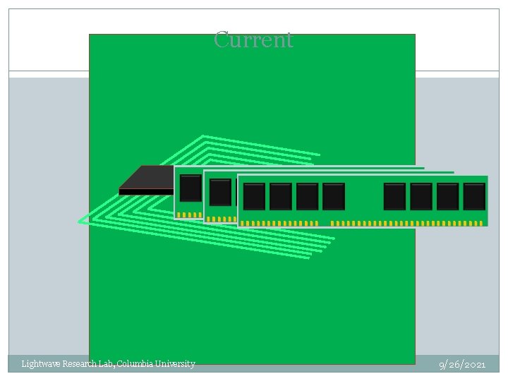
Current Lightwave Research Lab, Columbia University 9/26/2021

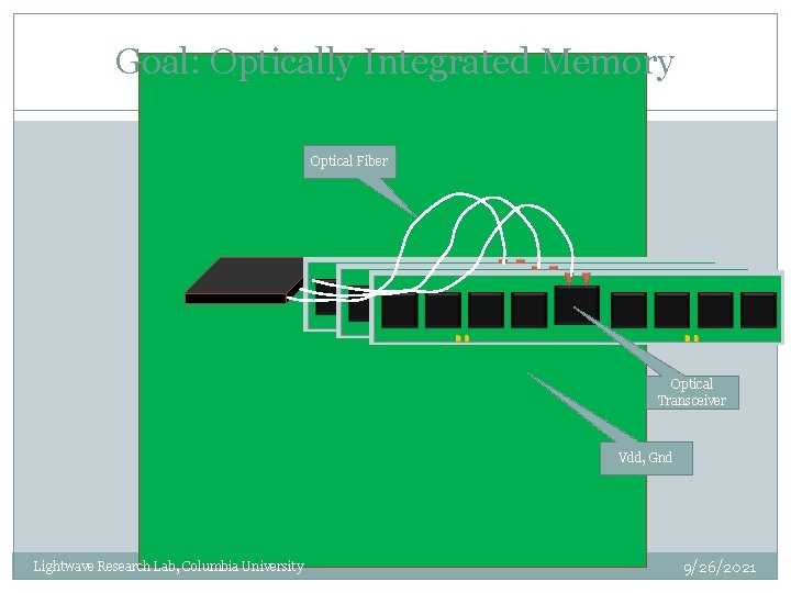
Goal: Optically Integrated Memory Optical Fiber Optical Transceiver Vdd, Gnd Lightwave Research Lab, Columbia University 9/26/2021

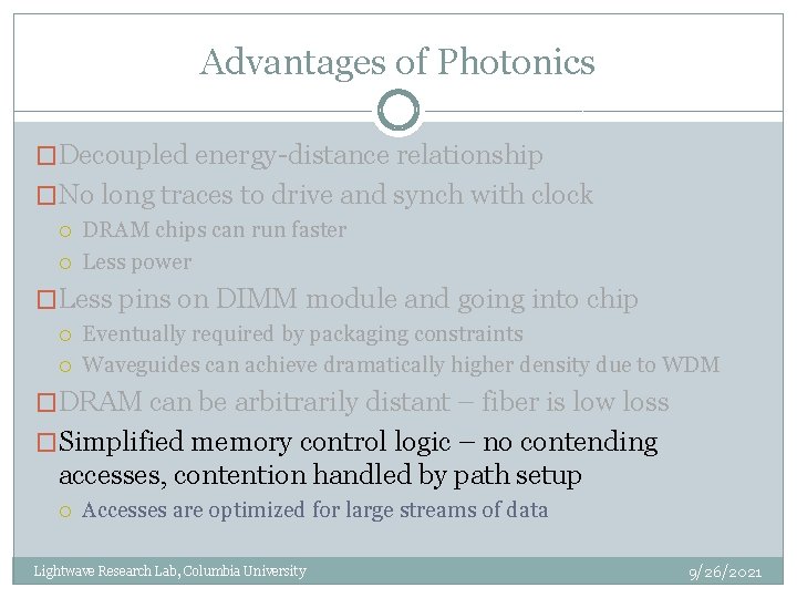
Advantages of Photonics �Decoupled energy-distance relationship �No long traces to drive and synch with clock DRAM chips can run faster Less power �Less pins on DIMM module and going into chip Eventually required by packaging constraints Waveguides can achieve dramatically higher density due to WDM �DRAM can be arbitrarily distant – fiber is low loss Lightwave Research Lab, Columbia University 9/26/2021
![Hybrid CircuitSwitched Photonic Network Broadband 1 2 Switch Cornell 2008 Transmission Broadband 2 2 Hybrid Circuit-Switched Photonic Network Broadband 1× 2 Switch [Cornell, 2008] Transmission Broadband 2× 2](https://slidetodoc.com/presentation_image_h2/be306fc2e68039069be1c53d19fd7185/image-14.jpg)
Hybrid Circuit-Switched Photonic Network Broadband 1× 2 Switch [Cornell, 2008] Transmission Broadband 2× 2 Switch Lightwave Research Lab, Columbia University [Shacham, NOCS ’ 07] 9/26/2021

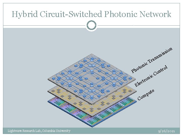
Hybrid Circuit-Switched Photonic Network ic n o t o Ph sm n ra on i s is T ic n o r ol r t on C t c Ele te u mp Co Lightwave Research Lab, Columbia University 9/26/2021

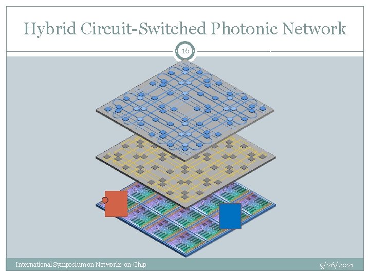
Hybrid Circuit-Switched Photonic Network 16 International Symposium on Networks-on-Chip 9/26/2021
![Hybrid CircuitSwitched Photonic Network 17 Bergman HPEC 07 International Symposium on NetworksonChip 9262021 Hybrid Circuit-Switched Photonic Network 17 [Bergman, HPEC ’ 07] International Symposium on Networks-on-Chip 9/26/2021](https://slidetodoc.com/presentation_image_h2/be306fc2e68039069be1c53d19fd7185/image-17.jpg)
Hybrid Circuit-Switched Photonic Network 17 [Bergman, HPEC ’ 07] International Symposium on Networks-on-Chip 9/26/2021

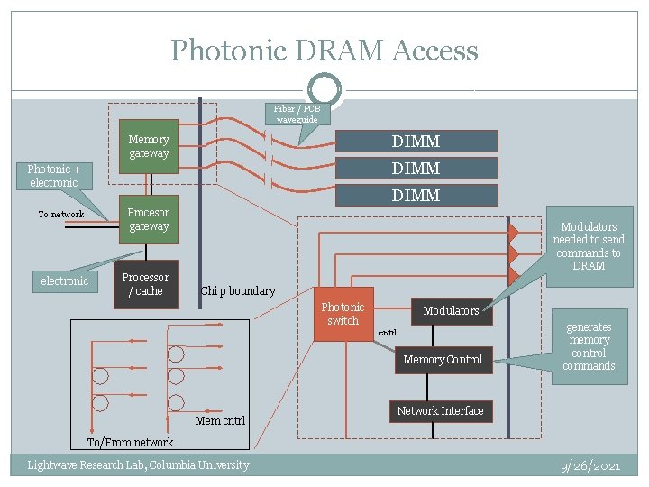
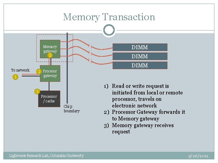
Photonic DRAM Access Fiber / PCB waveguide DIMM Memory gateway DIMM Photonic + electronic DIMM Procesor gateway To network electronic Processor / cache Modulators needed to send commands to DRAM Chi p boundary Photonic switch Modulators cntrl Memory Control Mem cntrl generates memory control commands Network Interface To/From network Lightwave Research Lab, Columbia University 9/26/2021

Memory Transaction DIMM Memory gateway 3 To network DIMM 2 Procesor gateway 1 1 Processor / cache Chi p boundary Lightwave Research Lab, Columbia University 1) Read or write request is initiated from local or remote processor, travels on electronic network 2) Processor Gateway forwards it to Memory gateway 3) Memory gateway receives request 9/26/2021

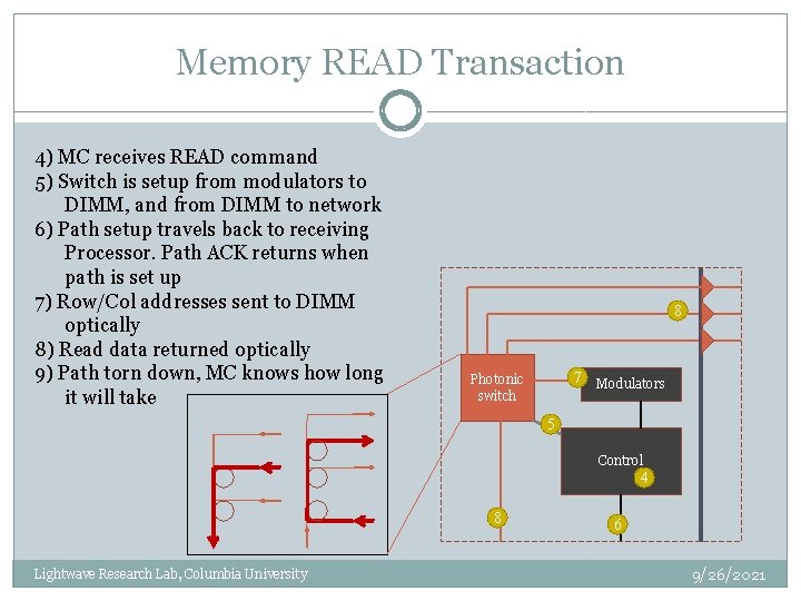
Memory READ Transaction 4) MC receives READ command 5) Switch is setup from modulators to DIMM, and from DIMM to network 6) Path setup travels back to receiving Processor. Path ACK returns when path is set up 7) Row/Col addresses sent to DIMM optically 8) Read data returned optically 9) Path torn down, MC knows how long it will take 8 7 Modulators Photonic switch 5 Control 4 8 Lightwave Research Lab, Columbia University 6 9/26/2021

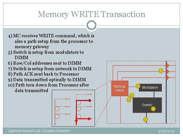
Memory WRITE Transaction 4) MC receives WRITE command, which is also a path setup from the processor to memory gateway 5) Switch is setup from modulators to DIMM 6) Row/Col addresses sent to DIMM 7) Switch is setup from network to DIMM 8) Path ACK sent back to Processor 9) Data transmitted optically to DIMM 10) Path torn down from Processor after data transmitted 9 6 Modulators Photonic switch 5 7 Control 4 8 Lightwave Research Lab, Columbia University 9/26/2021

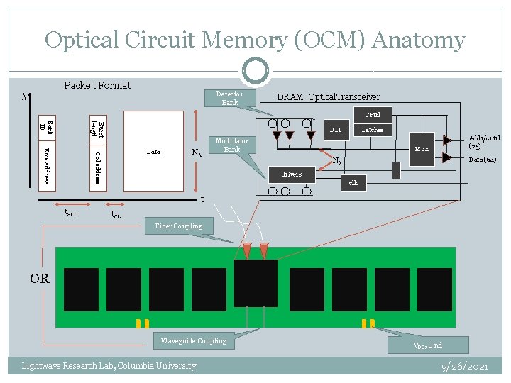
Optical Circuit Memory (OCM) Anatomy Packe t Format Detector Bank λ DRAM_Optical. Transceiver Cntrl Burst length Bank ID DLL Col address Row address Data Nλ Latches Modulator Bank Addr/cntrl (25) Mux Data (64) Nλ drivers clk t t. RCD t. CL Fiber Coupling OR Waveguide Coupling Lightwave Research Lab, Columbia University VDD, Gnd 9/26/2021

Advantages of Photonics �Decoupled energy-distance relationship �No long traces to drive and synch with clock DRAM chips can run faster Less power �Less pins on DIMM module and going into chip Eventually required by packaging constraints Waveguides can achieve dramatically higher density due to WDM �DRAM can be arbitrarily distant – fiber is low loss �Simplified memory control logic – no contending accesses, contention handled by path setup Accesses are optimized for large streams of data Lightwave Research Lab, Columbia University 9/26/2021

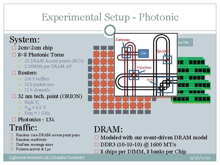
Experimental Setup - Photonic System: Photonic Torus Tile � 2 cm× 2 cm chip � 8× 8 Photonic Torus 28 DRAM Access points (MCs) 2 DIMMs per DRAM AP � Routers: 256 b buffers 32 b packet size 32 b channels � 32 nm tech. point (ORION) High Vt Vdd = 0. 8 V Freq = 1 GHz � Photonics - 13λ Traffic: � � Random core-DRAM access point pairs Random read/write Uniform message sizes Poisson arrival at 1µs Lightwave Research Lab, Columbia University DRAM: � Modeled with our event-driven DRAM model � DDR 3 (10 -10 -10) @ 1600 MT/s � 8 chips per DIMM, 8 banks per Chip 9/26/2021

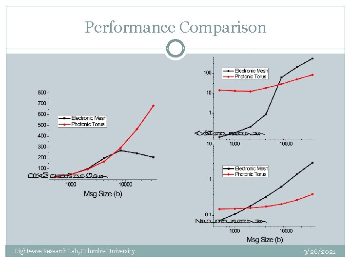
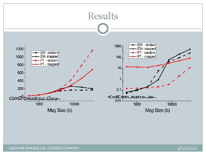
Performance Comparison Lightwave Research Lab, Columbia University 9/26/2021

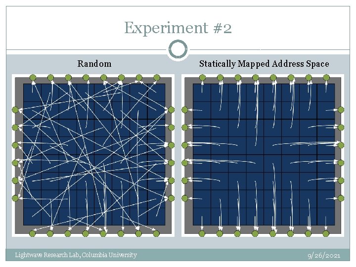
Experiment #2 Random Lightwave Research Lab, Columbia University Statically Mapped Address Space 9/26/2021

Results Lightwave Research Lab, Columbia University 9/26/2021

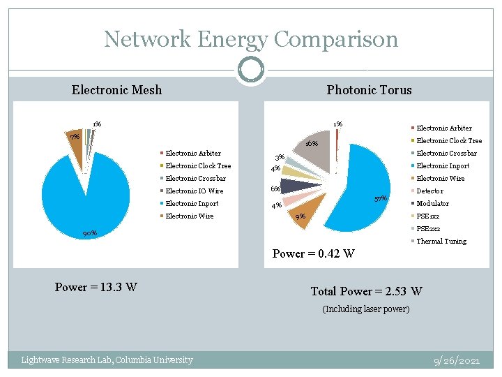
Network Energy Comparison Electronic Mesh Photonic Torus 1% 1% 7% Electronic Arbiter Electronic Clock Tree 16% Electronic Arbiter Electronic Clock Tree Electronic Crossbar 3% Electronic Inport 4% Electronic Crossbar Electronic Wire Electronic IO Wire 6% Electronic Inport 4% Electronic Wire 57% Detector Modulator PSE 1 x 2 9% PSE 2 x 2 90% Thermal Tuning Power = 0. 42 W Power = 13. 3 W Total Power = 2. 53 W (Including laser power) Lightwave Research Lab, Columbia University 9/26/2021

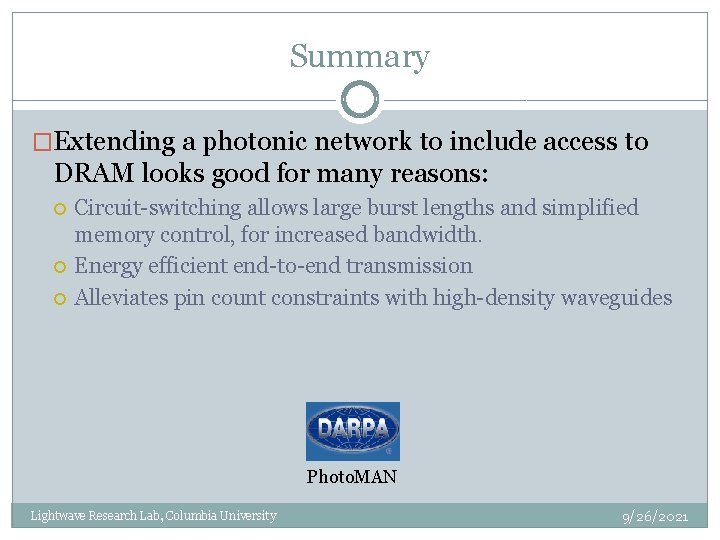
Summary �Extending a photonic network to include access to DRAM looks good for many reasons: Circuit-switching allows large burst lengths and simplified memory control, for increased bandwidth. Energy efficient end-to-end transmission Alleviates pin count constraints with high-density waveguides Photo. MAN Lightwave Research Lab, Columbia University 9/26/2021