Exploring Chip to Chip Photonic Networks Philip Watts

- Slides: 20

Exploring Chip to Chip Photonic Networks Philip Watts Computer Laboratory University of Cambridge Acknowledgement: Royal Commission for the Exhibition of 1851

Exploring Chip-to-Chip Photonics • Bandwidth improvements in electronic interconnects have been achieved at the expense of increased latency and power consumption • Photonics has the potential to reduce power consumption/ latency – Known for a long time, BUT size, cost, manufacturing issues – Enabling technologies: silicon photonics and 3 D integration • Needs a holistic, system assessment – assessing power consumption and performance

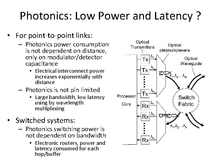
Photonics: Low Power and Latency ? • For point-to-point links: – Photonics power consumption is not dependent on distance, only on modulator/detector capacitance • Electrical interconnect power increases exponentially with distance – Photonics is not pin limited • Large bandwidth, low latency using by wavelength multiplexing • Switched systems: – Photonics switching power is not dependent on bandwidth • Electronic routers, power and latency consumed for each hop/buffer

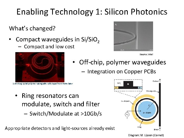
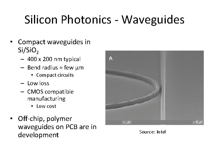
Enabling Technology 1: Silicon Photonics What’s changed? • Compact waveguides in Si/Si. O 2 – Compact and low cost Source: Intel • Off-chip, polymer waveguides – Integration on Copper PCBs 1. 4 m long spiral polymer waveguide with input from He. Ne laser • Ring resonators can modulate, switch and filter – Switch/Modulate at >10 Gb/s Appropriate detectors and light-sources already exist Diagram: M. Lipson (Cornell)

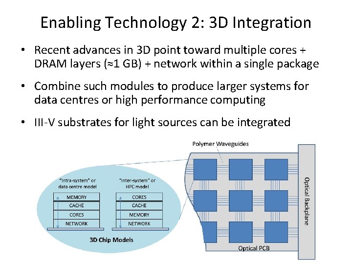
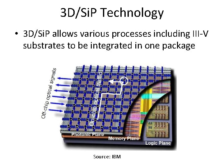
Enabling Technology 2: 3 D Integration • Recent advances in 3 D point toward multiple cores + DRAM layers (≈1 GB) + network within a single package • Combine such modules to produce larger systems for data centres or high performance computing • III-V substrates for light sources can be integrated

Characteristics of a Photonic Network • Photonic Limitations: – Signals can not be (practically) buffered – Difficult to read header and setup switch on the fly • These limitations leads naturally to circuit switching (with edge buffers) – Photonics is good for flows/large packets – Relatively inefficient for small packets (e. g. cache lines) • Obvious network choice: Central Xbar/Clos switch with time slot access, e. g. SWIFT (Intel/Cambridge) – Various alternative distributed approaches proposed

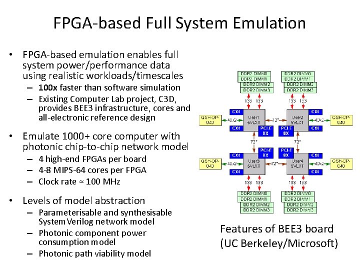
FPGA-based Full System Emulation • FPGA-based emulation enables full system power/performance data using realistic workloads/timescales – 100 x faster than software simulation – Existing Computer Lab project, C 3 D, provides BEE 3 infrastructure, cores and all-electronic reference design • Emulate 1000+ core computer with photonic chip-to-chip network model – 4 high-end FPGAs per board – 4 -8 MIPS-64 cores per FPGA – Clock rate ≈ 100 MHz • Levels of model abstraction – Parameterisable and synthesisable System. Verilog network model – Photonic component power consumption model – Photonic path viability model Features of BEE 3 board (UC Berkeley/Microsoft)

Exploring Chip-to-chip Photonics • Collaborators: Myself, Andrew Moore, Simon Moore (Cambridge), Robert Killey (UCL EE) • Program to investigate implications of chip-to-chip photonic interconnect on architecture of: – Data Centres – High Performance Computing • Build accurate and experimentally verified models of latest silicon photonics components (UCL) • Build full system FPGA-based emulator – Allows rapid network architectural exploration – Find applications which benefit from photonic networks

Backup

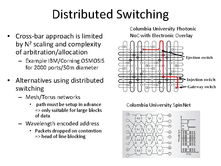
Distributed Switching • Cross-bar approach is limited by N 2 scaling and complexity of arbitration/allocation Columbia University Photonic No. C with Electronic Overlay – Example IBM/Corning OSMOSIS for 2000 ports/50 m diameter • Alternatives using distributed switching – Mesh/Torus networks • path must be setup in advance => only suitable for large blocks of data – Wavelength encoded address • Packets dropped on contention => head of line blocking Columbia University Spin. Net

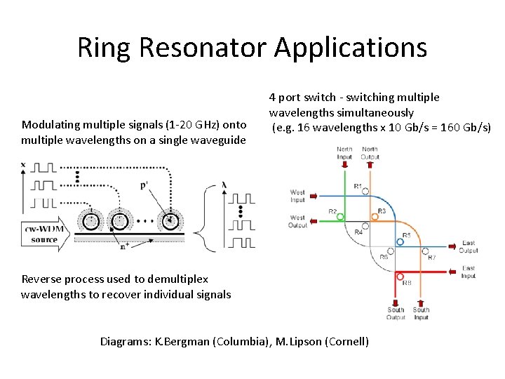
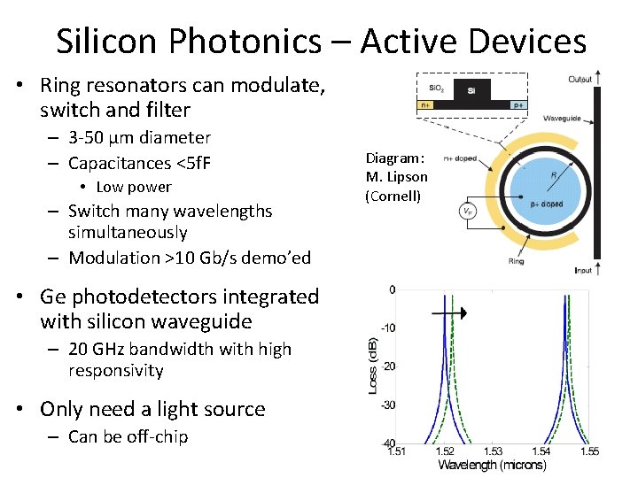
Ring Resonator Applications Modulating multiple signals (1 -20 GHz) onto multiple wavelengths on a single waveguide 4 port switch - switching multiple wavelengths simultaneously (e. g. 16 wavelengths x 10 Gb/s = 160 Gb/s) Reverse process used to demultiplex wavelengths to recover individual signals Diagrams: K. Bergman (Columbia), M. Lipson (Cornell)

3 D/Si. P Technology • 3 D/Si. P allows various processes including III-V substrates to be integrated in one package Source: IBM

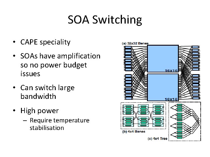
SOA Switching • CAPE speciality • SOAs have amplification so no power budget issues • Can switch large bandwidth • High power – Require temperature stabilisation

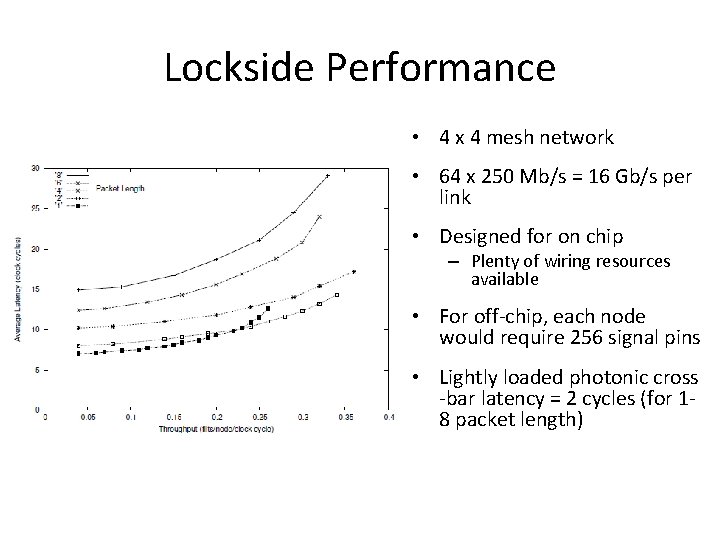
Lockside Performance • 4 x 4 mesh network • 64 x 250 Mb/s = 16 Gb/s per link • Designed for on chip – Plenty of wiring resources available • For off-chip, each node would require 256 signal pins • Lightly loaded photonic cross -bar latency = 2 cycles (for 18 packet length)

Example: Photonic Cross-bar • Min slot time = (RTT to switch) + (arbitration time) ≈ 15 ns for 1 m network radius – – Switching time with ring resonators is v. low Min latency = 2 slot times ≈ 30 ns 128 b packet only uses 800 ps! 15 ns also allows 280 B per slot (16λ x 10 Gb/s) • Currently creating initial model of chip-to-chip photonic network to add to C 3 D system – Compare with electronic VC router network • Initial design: – – – 32 Nodes each serving a 32 -core chip = 1000 cores 4 boards with 8 chips per board Central x-bar switch, centralised routing and arbitration, fixed time slots Network radius = 1 m Node bandwidth: 16 wavelengths at 5 -10 Gb/s each = 80 -160 Gb/s

Multiple Networks • An idea that repeatedly comes up in literature: Two networks – One for large packets/flows • Photonic, circuit switched or with long slot – One for short packets, could be: • Photonic with minimum slot time • Electronic • Point 2 point photonic • Local (covering a single PCB) and global networks – Centralised cross-bar removes locality • Additional networks for broadcast/multicast – High bandwidth photonic signals can be split many ways without impedance matching issues – However, power budgets! • This is an area where Semiconductor Optical Amps may be useful

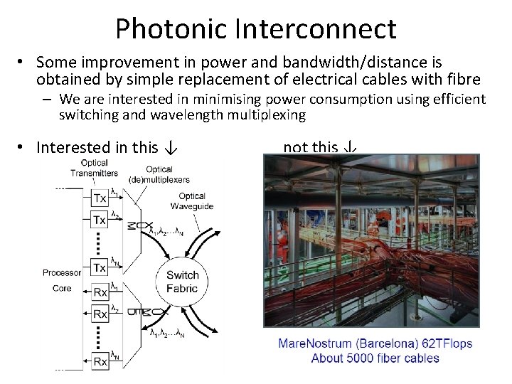
Photonic Interconnect • Some improvement in power and bandwidth/distance is obtained by simple replacement of electrical cables with fibre – We are interested in minimising power consumption using efficient switching and wavelength multiplexing • Interested in this ↓ not this ↓

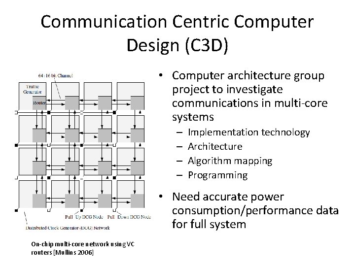
Communication Centric Computer Design (C 3 D) • Computer architecture group project to investigate communications in multi-core systems – – Implementation technology Architecture Algorithm mapping Programming • Need accurate power consumption/performance data for full system On-chip multi-core network using VC routers [Mullins 2006]

Silicon Photonics - Waveguides • Compact waveguides in Si/Si. O 2 – 400 x 200 nm typical – Bend radius ≈ few μm • Compact circuits – Low loss – CMOS compatible manufacturing • Low cost • Off-chip, polymer waveguides on PCB are in development Source: Intel

Silicon Photonics – Active Devices • Ring resonators can modulate, switch and filter – 3 -50 μm diameter – Capacitances <5 f. F • Low power – Switch many wavelengths simultaneously – Modulation >10 Gb/s demo’ed • Ge photodetectors integrated with silicon waveguide – 20 GHz bandwidth with high responsivity • Only need a light source – Can be off-chip Diagram: M. Lipson (Cornell)